EP0466495A2 - Dispositif d'affichage à cristal liquide - Google Patents
Dispositif d'affichage à cristal liquide Download PDFInfo
- Publication number
- EP0466495A2 EP0466495A2 EP91306328A EP91306328A EP0466495A2 EP 0466495 A2 EP0466495 A2 EP 0466495A2 EP 91306328 A EP91306328 A EP 91306328A EP 91306328 A EP91306328 A EP 91306328A EP 0466495 A2 EP0466495 A2 EP 0466495A2
- Authority
- EP
- European Patent Office
- Prior art keywords
- liquid crystal
- film
- storage capacity
- display apparatus
- crystal display
- Prior art date
- Legal status (The legal status is an assumption and is not a legal conclusion. Google has not performed a legal analysis and makes no representation as to the accuracy of the status listed.)
- Granted
Links
Images


Classifications
-
- G—PHYSICS
- G02—OPTICS
- G02F—OPTICAL DEVICES OR ARRANGEMENTS FOR THE CONTROL OF LIGHT BY MODIFICATION OF THE OPTICAL PROPERTIES OF THE MEDIA OF THE ELEMENTS INVOLVED THEREIN; NON-LINEAR OPTICS; FREQUENCY-CHANGING OF LIGHT; OPTICAL LOGIC ELEMENTS; OPTICAL ANALOGUE/DIGITAL CONVERTERS
- G02F1/00—Devices or arrangements for the control of the intensity, colour, phase, polarisation or direction of light arriving from an independent light source, e.g. switching, gating or modulating; Non-linear optics
- G02F1/01—Devices or arrangements for the control of the intensity, colour, phase, polarisation or direction of light arriving from an independent light source, e.g. switching, gating or modulating; Non-linear optics for the control of the intensity, phase, polarisation or colour
- G02F1/13—Devices or arrangements for the control of the intensity, colour, phase, polarisation or direction of light arriving from an independent light source, e.g. switching, gating or modulating; Non-linear optics for the control of the intensity, phase, polarisation or colour based on liquid crystals, e.g. single liquid crystal display cells
- G02F1/133—Constructional arrangements; Operation of liquid crystal cells; Circuit arrangements
- G02F1/136—Liquid crystal cells structurally associated with a semi-conducting layer or substrate, e.g. cells forming part of an integrated circuit
- G02F1/1362—Active matrix addressed cells
- G02F1/136213—Storage capacitors associated with the pixel electrode
-
- H—ELECTRICITY
- H10—SEMICONDUCTOR DEVICES; ELECTRIC SOLID-STATE DEVICES NOT OTHERWISE PROVIDED FOR
- H10D—INORGANIC ELECTRIC SEMICONDUCTOR DEVICES
- H10D30/00—Field-effect transistors [FET]
- H10D30/60—Insulated-gate field-effect transistors [IGFET]
- H10D30/67—Thin-film transistors [TFT]
- H10D30/6729—Thin-film transistors [TFT] characterised by the electrodes
- H10D30/673—Thin-film transistors [TFT] characterised by the electrodes characterised by the shapes, relative sizes or dispositions of the gate electrodes
Definitions
- the present invention relates to an active matrix type liquid crystal display apparatus.
- An active matrix type liquid crystal display (LCD) apparatus which is provided with thin film transistors (TFT's) formed with an amorphous silicone (a-Si) film as switching devices has gained public attention.
- TFT's thin film transistors
- a-Si amorphous silicone
- Fig. 1 is an equivalent circuit of a picture element of a substrate for liquid crystal driving semiconductor device used for such a liquid crystal apparatus.
- a floating capacity C gs
- a storage capacity C s
- reference numeral 1 is an address line
- reference numeral 2 is a data line.
- FIG. 2 The sectional view of the substrate for liquid crystal driving semiconductor device array which constracts the above mentioned picture element circuit is shown in Fig. 2, for example.
- the TFT drain electrode 2a is connected to the data line 2.
- the source electrode 2b
- the display electrode 6 and the insulator film 4 which is formed under the display electrode 6 (hereinafter the insulation film 4 is named the first insulation film) are coated with a second insulation film 7 except for the portion for connecting the display electrode 6 and the source electrode 2b, the second insulation film 7 preventing such a point defect from taking place.
- the inter-layer insulation film is formed with two layers of the first insulation film 4 and the second insulation film 7, the following drawbacks result in.
- the second insulation film 7 is formed by CVD method or plasma CVD method. Since such an equipment is expensive, twice deposition of the CVD film will increase the production cost.
- the thickness of the insulator film between the gate electrode line 1a and the semiconductor thin film 5 it is necessary to decrease the thickness of the first insulation film 4. Thus, a shortcircuit tends to take place between the display electrode 6 and the storage capacity line 1b.
- ⁇ s is the dielectric constant of the insulation film, d the film thickness, S, the area of the electrode, and ⁇ 0 the dielectric constant of vacuum, respectively.
- Cs ⁇ 0 ⁇ s / (d x S)
- the dielectric constant of the insulation film, ⁇ s depends on the material.
- the dielectric constant is 4.
- SiN x it is 7.
- the film thickness, d cannot be remarkably decreased due to restrictions of the breakdown voltage, leak current, and the pin hole density.
- the area of the electrode, S should be decreased so as to improve the aperture ratio.
- an insulation film with a high dislsctric constant is required.
- the increase of the aperture ratio is further required with decreasing the size of picture elements.
- ⁇ V d is a voltage drop due to a switching
- C gs is a floating capacity between the gate and the source
- C LC is a capacity of the liquid crystal layer
- C s is the value of storage capacity
- V g is a gate pulse voltage.
- a substrate for liquid crystal driving semiconductor device where the display electrode 6 is coated with an insulator film has been studied.
- two layers as the inter-layer insulator film should be deposited by means of the CVD method or the plasma CVD method which requires expensive equipment.
- a shortcircuit tends to take place between the storage capacity line 1b and the display electrode 6.
- an object of the present invention is to provide a liquid crystal display apparatus with s small area of a storage capacity line so as to improve the aperture ratio.
- Another object of the present invention is to provide a liquid crystal display apparatus for clearly displaying a picture with small picture elements for accomplishing a high definition display.
- Another object of the present invention is to provide a liquid crystal display apparatus for completely preventing a shortcircuit between a storage capacity line and a display electrode.
- Another object of the present invention is to provide a liquid crystal display apparatus which can be produced with a high cost performance.
- the liquid crystal display apparatus has a substrate for liquid crystal driving semiconductor device with a display picture elements having driving thin film transistors and storage capacity devices, the display picture elements being disposed on one major surface of a transparent substrate, wherein the storage capacity device comprises a storage capacity metallic line made of a metal containing Ta and N, the storage capacity metallic line being disposed on the one major surface of the transparent substrate, an anodic oxide of the metal film formed on the surface of the storage capacity metallic line, and a display electrode in contact with the anodic oxide film.
- the metal containing Ta and N according to the present invention is a metal which contains of Ta, Mo-Ta, W-Ta, Nb-Ta, Al-W-Ta, Al-Nb-Ta, Ti-W-Ta, Ti-Nb-Ta, Zr-W-Ta, Zr-Nb-Ta, or the like, and contains N.
- the dielectric constant of the metallic anodic oxidization film of the liquid crystal display apparatus is larger than that of a SiO x film and a SiN x film made by the conventional CVD method and the plasma CVD method, the area of the storage capacity electrode can be decreased and thereby improving the aperture ratio.
- the dielectric constant of the SiO x film is 4 and that of the SiN x film is 7.
- the anodic oxide films have a high dielectric constant.
- the dielectric constant of an AlO x film is 8; that of a TaO x is 30; that of a Ta-N-O film ranges from 10 to 30; that of a TiO x film is 80; and that of a ZrO x film is 9.
- the liquid crystal display apparatus can be produced at a lower cost than that which uses the insulator films formed by means of the conventional CVD plasma method and the CVD method.
- the metallic anodic oxidization film is free from pin holes, even if it is formed as a thin film, a shortcircuit does not take place between the storage capacity line and the picture element electrode.
- the CVD film and the plasma CVD film are formed by deposition, occurrence of pin holes due to deposited particles is inevitable.
- the anodic oxide film is oxidized from its surface, it has a self repair action and thereby pin holes do not take place. Thus, even if the anodic oxide film is formed as a thin film, no defects take place.
- Fig. 4 is a sectional view showing a construction of the principal portion of a substrate for liquid crystal driving semiconductor device used in an embodiment according to the present invention.
- a gate electrode line 11a, a storage capacity line 11b, and an address line 11 which are made of a metallic wiring material, for example, Ta 0.8 N 0.2 are disposed on one surface of a transparent substrate 13, for example, a glass substrate.
- the surfaces of the lines 11a, 11b, and 11 are coated with an anodic oxide film 18, for example, a Ta-N-O film.
- a display electrode 16 is formed with a display electrode material, for example, ITO (In2O3-SnO2).
- the display electrode 16 and the gate electrode line 11a are coated with an insulator film 14, for example, an SiO x film.
- An a-Si film 15a and an n+a-Si film 15b, for example, are formed in the order on the gate electrode line 11a through the insulator film 14.
- a drain electrode 12a and a source electrode 12b are formed by, for example, Al/Mr.
- the drain electrode 12a is connected to a data line 12 formed on the insulator film 14.
- the source electrode 12b is connected to the display electrode 16 through a through-hole made on the insulator film 14 disposed on the display electrode 16. Thereafter, the n+a-Si film is removed as a channel portion and thereby a TFT is formed.
- the dielectric constant of a TaNO film is in the range from 10 to 30 and that of a TaO x film is 30.
- the dielectric constant of a SiO x film is 4 and that of a SiN x film is 7.
- the dielectric constant of the former is larger than that of the latter.
- the area of the storage capacity line 11b can be decreased (in the case of the TaO x film, its area can be decreased to approx. 1/7 times that of the SiO x film; and in the case of a (Ta 0.8 N 0.2 ) x O y film, its area can be decreased to approx. 1/6 times that of the SiO x film).
- the aperture ratio can be accordingly improved.
- the TaO x film As an anodic oxidization film, it is possible to use the TaO x film instead of the TaNO film. However, in this construction, since the leak current becomes large, it is necessary to raise the anodization voltage of the anode film to around 200 V so as to satisfy the condition of ⁇ Thus, the thickness of the TaO x film becomes twice that of the TaNO film. Thus, the capacity becomes half. In addition, the step between lines becomes large. Thus, the data line tends to break.
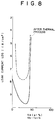
- Fig. 5 shows the dependence of resistivity of the TaNO film against the composition and anodization voltage.
- the leak current of the storage capacity is calculated by using a required resistivity, it should be 2 x 10 ⁇ 6 A/cm2 or less (the resistivity should be 1.2 x 10¹¹ ⁇ cm or greater). (These values vary to some extent depending on the size of TFT, the frame frequency, and so forth.)
- the condition of the leak current is satisfied.
- the condition of the leak current is not satisfied.
- the insulator film is formed with TaNO x , since the thickness can be decreased, it is possible to provide it with large storage capacity by using the same area.
- the leak current readily increases depending on the spatter condition of Ta and presence of a small amount of impurities.
- the leak current becomes stable with a small value.
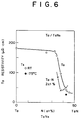
- Fig. 6 shows the relationship between the composition and the resistivity in the case where a Ta layer formed with an lower layer film of TaN x and an upper layer where Ta is spattered thereon is changed from ⁇ -Ta with high resistivity to ⁇ -Ta with low resistivity.
- the resistance of the lines can be decreased.
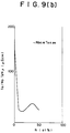
- Figs. 7 and 8 show the leak current of anodic oxide films of an Nb-Ta alloy compounded with N (in Fig. 7, Nb x Ta y N 0.2 ; and in Fig. 8, Ta 0.85 Nb 0.15 ) x N y ) tends to decrease with increasing N like the case of TaN x .
- Figs. 9 (a) and 9 (b) show the relationship between the composition of the lower layer film of NbTaN x and the resistivity of the Ta layer formed as the upper layer. In this construction (lamination), the resistance of the Ta layer becomes low. In other words, when Nb is alloyed, even if the additive amount of N is small (10 atomic % or less), the resistance of Ta becomes low.
- a Ta-Nb-N film, a Ta-Mo-N alloy film, a Ta-W-N alloy film, and so forth, where the leak current of the anodic oxidization film is small can be used as a metal of the lower layer.
- the amount of N which satisfies the above mentioned condition also depends on the production condition, it is preferably in the range from 5 to 45 atomic %.
- the amounts of Nb, Mo, and W are preferably up to 50 atomic %.
- a metallic wiring material for example, Ta-N, is layered with a thickness of 300 nm by sputtering method on the transparent substrate 13, for example, a glass substrate. Thereafter, the metallic wiring material is patterned and then etched so as to form the gate electrode line 11a, the storage capacity line 11b, and the address line 11.
- the electrode 11a, 11b, and 11 are oxidized in citric acid with a constant current of 0.5 mA/cm2 until the voltage becomes 100 V.
- the lines 11a, 11b, and 11 are oxidized with a constant voltage of 100 V.
- the anodic oxide film 18, for example, a TaNO film with a thickness of 200 nm is formed on the surfaces of the lines 11a, 11b, and 11.
- a display electrode material for example, an ITO film with a thickness of 100 nm, is formed on the anodic oxide film 18 over the storage capacity line 11b by the sputtering method.
- the display electrode material is patterned and then etched so as to form the display electrode 16.
- a SiO x film with a thickness of approx. 300 nm is formed by, for example, the plasma CVD method.
- the through-hole 19 is made by, for example, the etching process.
- the a-Si film 15a with a thickness of 300 nm and the n+ a-Si film 15b with a thickness of 50 nm are formed in the order on the insulator film 14 by, for example, the plasma CVD method so as to form an island of a-Si.
- electrode materials for example, Mo and Al, are formed with a thickness of approx. 1 ⁇ m by the sputtering method.
- the line materials are patterned and then etched so as to form the drain electrode 12a, the source electrode 12b, and the data line 12.
- the n+ a-Si film 15b at the channel portion is etched and thereby the substrate for liquid crystal driving semiconductor device in the above mentioned construction is produced.
- Fig. 10 shows another example of a construction of the substrate for liquid crystal driving semiconductor device.
- Al 11′ is formed on the transparent substrate 13, for example, the glass substrate, by the sputtering method so as to decrease the resistance of the lines.
- the Al 11′ is patterned and then coated with Ta, TaN x , or the like.
- the substrate is produced in the same manner as the above mentioned embodiment.
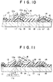
- Fig. 11 is a sectional view showing a substrate for liquid crystal driving semiconductor device of another embodiment according to the present invention.
- alloys 11a′, 11b′, and 11c′ which are compounded with Ta-N, Mo-Ta-N, Nb-Ta-N, W-Ta-N, or a combination thereof are deposited as base metals for 30 nm on the glass substrate 13, for example. Thereafter, the Ta layers 11a ⁇ , 11b ⁇ , and 11c ⁇ with a low resistance are laminated on the alloys 11a′, 11b′, and 11c′, respectively.
- alloy layers 11a ⁇ ′, 11b ⁇ ′, and 11c ⁇ ′ which are compounded with Ta-N, Mo-Ta-N, Nb-Ta-N, or W-Ta-N are laminated for 100 nm on the Ta layers 11a ⁇ , 11b ⁇ , and 11c ⁇ , respectively. Thereafter, the surfaces of the alloy layers 11a ⁇ ′, 11b ⁇ ′, and 11c ⁇ ′ are anodically oxidized. Thereafter, in the same manner as the above embodiment 1, the substrate is produced.
- a tetragonal Ta ( ⁇ -Ta) is normally formed by the sputtering method.
- a cubic Ta ( ⁇ -Ta) layers 11a ⁇ , 11b ⁇ , and 11c ⁇ with a low resistance can be formed.
- the anodic oxide films of the alloys 11a ⁇ ′, 11b ⁇ ′, and 11c ⁇ ′, where N is alloyed with Mo-Ta, Nb-Ta, or W-Ta, and which are formed on the Ta layers 11a ⁇ , 11b ⁇ , and 11c ⁇ have a high insulator resistance like the TaN x anodic oxide film.
- the same effect can be obtained.
- the base metal layers 11a′, 11b′, and 11c′ function as etching stoppers of the glass substrate 13.
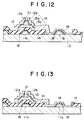
- Fig. 12 is a sectional view showing a substrate for liquid crystal driving semiconductor device of another embodiment according to the present invention.
- the substrate is produced and constructed in the process similar to that of the above mentioned embodiments except that after TFT is formed, the insulator film of the picture element portion is etched and removed so as to prevent a voltage applied to a liquid crystal of an insulator film on the display electrode 16 made of ITO from decreasing.
- Fig. 13 shows an example of a substrate which is constructed in the manner that the gate insulator film of the storage capacity C s is removed and then the display electrode 16 made of ITO is formed.
- Fig. 12 shows an example of a substrate which is constructed in the manner that the gate insulator film of the storage capacity C s is removed and then the display electrode 16 made of ITO is formed.
- a passivation insulator film 20 is formed besides the electrode 16 for the storage capacity C s and then the display electrode 16 is formed on the surface so as to remove a gap of the display portion.
- the liquid crystal display apparatus is formed by injecting liquid crystal between the array substrate (substrate for liquid crystal driving semiconductor device) and the counter electrode plate.
- reference numeral 21 is a stopper insulator film disposed on the surface of the semiconductor thin film 15.
- the channel portion may be constructed not only in back channel cut type where the channel portion is etched, but in the type where a stopper made of an insulator film is disposed on the channel. Moreover, staggered type where the gate is disposed at the top may be used. Furthermore, the semiconductor may be not only a-Si, but p-Si and CdSe. The insulator film at the display portion on ITO can be etched and then removed.
- the gate electrode line 11a, the storage capacity line 11b, and the address line 11 may be not only Ta and TaN x , but a metal which can be anodically oxidized.
- the metals which can be anodically oxidized are Ta, Mo-Ta, W-Ta, Ta-N, Al, Ti, Zr, and alloys thereof.
- the lines 11a, 11b, and 11 may be laminates of such materials.
- the solution used for anodically oxidizing such metals and alloys may be not only citric acid, but phosphoric acid. In any case, the solution to be used may be a solution suitable for the metals in use.
- the insulator film 14 may be not only SiO x formed by the plasma CVD method, but SiO x and SiN x formed by various film forming methods or lamination films thereof.
- the display electrode may be not only ITO, but a metal.
- the permittivity of the anodic oxide film is high, the area of the storage capacity electrode can be decreased and thereby the aperture ratio can be accordingly improved.
- the area of the storage capacity electrode according to the present invention is remarkably decreased in comparison with that of the insulator film of SiO x or SiN x .
- the aperture ratio is improved by around twice.
- the liquid crystal display apparatus according to the present invention uses the anodic oxide film which is free from pin holes and which can be formed by inexpensive equipment, it is free from defect. In addition, the production cost does not rise. Moreover, shortcircuit does not take place in the storage capacity portion.
Landscapes
- Physics & Mathematics (AREA)
- Nonlinear Science (AREA)
- Engineering & Computer Science (AREA)
- Crystallography & Structural Chemistry (AREA)
- Mathematical Physics (AREA)
- Chemical & Material Sciences (AREA)
- General Physics & Mathematics (AREA)
- Optics & Photonics (AREA)
- Microelectronics & Electronic Packaging (AREA)
- Power Engineering (AREA)
- Liquid Crystal (AREA)
- Thin Film Transistor (AREA)
- Insulated Gate Type Field-Effect Transistor (AREA)
- Devices For Indicating Variable Information By Combining Individual Elements (AREA)
Applications Claiming Priority (4)
| Application Number | Priority Date | Filing Date | Title |
|---|---|---|---|
| JP185736/90 | 1990-07-12 | ||
| JP18573690 | 1990-07-12 | ||
| JP12771691A JP3226223B2 (ja) | 1990-07-12 | 1991-05-30 | 薄膜トランジスタアレイ装置および液晶表示装置 |
| JP127716/91 | 1991-05-30 |
Publications (3)
| Publication Number | Publication Date |
|---|---|
| EP0466495A2 true EP0466495A2 (fr) | 1992-01-15 |
| EP0466495A3 EP0466495A3 (en) | 1992-09-23 |
| EP0466495B1 EP0466495B1 (fr) | 1995-06-21 |
Family
ID=26463601
Family Applications (1)
| Application Number | Title | Priority Date | Filing Date |
|---|---|---|---|
| EP91306328A Expired - Lifetime EP0466495B1 (fr) | 1990-07-12 | 1991-07-12 | Dispositif d'affichage à cristal liquide |
Country Status (5)
| Country | Link |
|---|---|
| US (1) | US5187602A (fr) |
| EP (1) | EP0466495B1 (fr) |
| JP (1) | JP3226223B2 (fr) |
| KR (1) | KR950006028B1 (fr) |
| DE (1) | DE69110563T2 (fr) |
Cited By (7)
| Publication number | Priority date | Publication date | Assignee | Title |
|---|---|---|---|---|
| EP0566408A1 (fr) * | 1992-04-15 | 1993-10-20 | Kabushiki Kaisha Toshiba | Dispositif d'affichage à cristaux liquides |
| EP0592063A3 (en) * | 1992-09-14 | 1994-07-13 | Toshiba Kk | Active matrix liquid crystal display device |
| EP0709718A3 (fr) * | 1994-10-28 | 1997-03-19 | Hitachi Ltd | Dispositif d'affichage à cristal liquide et son procédé de fabrication |
| KR100430744B1 (ko) * | 1995-06-14 | 2004-08-25 | 가부시끼가이샤 히다치 세이사꾸쇼 | 고집적도대면적lcd디스플레이용tft패널과그제조방법및액정표시장치 |
| US6862050B2 (en) | 1996-11-26 | 2005-03-01 | Samsung Electronics Co., Ltd. | Liquid crystal displays using organic insulating material for a gate insulating layer and/or having photolithographic formed spacers |
| US6940566B1 (en) | 1996-11-26 | 2005-09-06 | Samsung Electronics Co., Ltd. | Liquid crystal displays including organic passivation layer contacting a portion of the semiconductor layer between source and drain regions |
| US8003989B2 (en) | 1999-08-12 | 2011-08-23 | Semiconductor Energy Laboratory Co., Ltd. | Thin film semiconductor device having a terminal portion |
Families Citing this family (44)
| Publication number | Priority date | Publication date | Assignee | Title |
|---|---|---|---|---|
| JP2620240B2 (ja) | 1987-06-10 | 1997-06-11 | 株式会社日立製作所 | 液晶表示装置 |
| US5402254B1 (en) * | 1990-10-17 | 1998-09-22 | Hitachi Ltd | Liquid crystal display device with tfts in which pixel electrodes are formed in the same plane as the gate electrodes with anodized oxide films before the deposition of silicon |
| US6713783B1 (en) | 1991-03-15 | 2004-03-30 | Semiconductor Energy Laboratory Co., Ltd. | Compensating electro-optical device including thin film transistors |
| JP2873632B2 (ja) | 1991-03-15 | 1999-03-24 | 株式会社半導体エネルギー研究所 | 半導体装置 |
| US5274485A (en) * | 1991-06-24 | 1993-12-28 | Sanyo Electric Co., Ltd. | Liquid crystal display |
| US6979840B1 (en) * | 1991-09-25 | 2005-12-27 | Semiconductor Energy Laboratory Co., Ltd. | Thin film transistors having anodized metal film between the gate wiring and drain wiring |
| EP0545327A1 (fr) * | 1991-12-02 | 1993-06-09 | Matsushita Electric Industrial Co., Ltd. | Réseau de transistors à couche mince pour une utilisation dans un afficheur à cristaux liquides |
| JP3133140B2 (ja) * | 1992-04-01 | 2001-02-05 | 株式会社半導体エネルギー研究所 | 表示装置 |
| JP2907629B2 (ja) * | 1992-04-10 | 1999-06-21 | 松下電器産業株式会社 | 液晶表示パネル |
| JP3245959B2 (ja) * | 1992-06-05 | 2002-01-15 | 松下電器産業株式会社 | 液晶画像表示装置の製造方法 |
| JPH05341315A (ja) * | 1992-06-08 | 1993-12-24 | Hitachi Ltd | 薄膜トランジスタ基板、液晶表示パネルおよび液晶表示装置 |
| JP3529153B2 (ja) * | 1993-03-04 | 2004-05-24 | 三星電子株式会社 | 液晶表示装置及びその製造方法 |
| JPH06347827A (ja) * | 1993-06-07 | 1994-12-22 | Hitachi Ltd | 液晶表示装置およびその製造方法 |
| KR100359795B1 (ko) * | 1995-08-22 | 2003-01-14 | 엘지.필립스 엘시디 주식회사 | 액정표시장치및그제조방법 |
| JPH0980416A (ja) * | 1995-09-13 | 1997-03-28 | Sharp Corp | 液晶表示装置 |
| KR100223899B1 (ko) * | 1996-01-15 | 1999-10-15 | 구자홍 | 액정표시장치의 구조 및 제조방법 |
| JP3222762B2 (ja) * | 1996-04-26 | 2001-10-29 | シャープ株式会社 | アクティブマトリクス基板およびその製造方法 |
| JPH1020331A (ja) * | 1996-06-28 | 1998-01-23 | Sharp Corp | 液晶表示装置 |
| KR100209620B1 (ko) * | 1996-08-31 | 1999-07-15 | 구자홍 | 액정 표시 장치 및 그 제조방법 |
| KR100241287B1 (ko) * | 1996-09-10 | 2000-02-01 | 구본준 | 액정표시소자 제조방법 |
| US6044128A (en) * | 1997-02-04 | 2000-03-28 | Kabushiki Kaisha Toshiba | X-ray imaging apparatus and X-ray imaging analysis apparatus |
| JPH10319428A (ja) * | 1997-05-19 | 1998-12-04 | Toshiba Corp | アクティブマトリクス型液晶表示装置 |
| JP4324259B2 (ja) * | 1998-07-07 | 2009-09-02 | シャープ株式会社 | 液晶表示装置の製造方法 |
| JP3592535B2 (ja) | 1998-07-16 | 2004-11-24 | 株式会社半導体エネルギー研究所 | 半導体装置の作製方法 |
| US6909114B1 (en) | 1998-11-17 | 2005-06-21 | Semiconductor Energy Laboratory Co., Ltd. | Semiconductor device having LDD regions |
| US6365917B1 (en) * | 1998-11-25 | 2002-04-02 | Semiconductor Energy Laboratory Co., Ltd. | Semiconductor device |
| US6469317B1 (en) | 1998-12-18 | 2002-10-22 | Semiconductor Energy Laboratory Co., Ltd. | Semiconductor device and method of fabricating the same |
| US6515648B1 (en) * | 1999-08-31 | 2003-02-04 | Semiconductor Energy Laboratory Co., Ltd. | Shift register circuit, driving circuit of display device, and display device using the driving circuit |
| KR100351440B1 (ko) * | 1999-12-31 | 2002-09-09 | 엘지.필립스 엘시디 주식회사 | 엑스-선 검출소자 및 그의 제조방법 |
| JP3720689B2 (ja) * | 2000-07-31 | 2005-11-30 | キヤノン株式会社 | インクジェットヘッド用基体、インクジェットヘッド、インクジェットヘッドの製造方法、インクジェットヘッドの使用方法およびインクジェット記録装置 |
| US6465286B2 (en) * | 2000-12-20 | 2002-10-15 | General Electric Company | Method of fabricating an imager array |
| US7095460B2 (en) * | 2001-02-26 | 2006-08-22 | Samsung Electronics Co., Ltd. | Thin film transistor array substrate using low dielectric insulating layer and method of fabricating the same |
| KR20030027302A (ko) * | 2001-09-28 | 2003-04-07 | 삼성전자주식회사 | 저유전율 절연막을 사용하는 박막 트랜지스터 기판 및 그제조 방법 |
| SG116443A1 (en) * | 2001-03-27 | 2005-11-28 | Semiconductor Energy Lab | Wiring and method of manufacturing the same, and wiring board and method of manufacturing the same. |
| KR100796749B1 (ko) | 2001-05-16 | 2008-01-22 | 삼성전자주식회사 | 액정 표시 장치용 박막 트랜지스터 어레이 기판 |
| US7172947B2 (en) * | 2004-08-31 | 2007-02-06 | Micron Technology, Inc | High dielectric constant transition metal oxide materials |
| JP2007027773A (ja) * | 2006-08-28 | 2007-02-01 | Semiconductor Energy Lab Co Ltd | 半導体装置及びその作製方法 |
| CN101819363B (zh) | 2009-02-27 | 2011-12-28 | 北京京东方光电科技有限公司 | Tft-lcd阵列基板及其制造方法 |
| JP5604087B2 (ja) * | 2009-11-27 | 2014-10-08 | 株式会社半導体エネルギー研究所 | 半導体装置の作製方法 |
| KR101835525B1 (ko) * | 2011-02-17 | 2018-04-20 | 삼성디스플레이 주식회사 | 표시 장치 및 그 제조 방법 |
| CN103243303B (zh) * | 2013-04-19 | 2015-06-03 | 江苏科技大学 | 一种Ta-Mo-N复合涂层及其制备方法 |
| JP2017078864A (ja) * | 2016-11-30 | 2017-04-27 | 株式会社半導体エネルギー研究所 | 液晶表示装置 |
| JP2019023734A (ja) * | 2018-08-24 | 2019-02-14 | 株式会社半導体エネルギー研究所 | 液晶表示装置 |
| CN111106261B (zh) * | 2019-12-06 | 2021-02-26 | 深圳市华星光电半导体显示技术有限公司 | 显示面板及显示装置 |
Family Cites Families (12)
| Publication number | Priority date | Publication date | Assignee | Title |
|---|---|---|---|---|
| GB2056739B (en) * | 1979-07-30 | 1984-03-21 | Sharp Kk | Segmented type liquid crystal display and driving method thereof |
| FR2527385B1 (fr) * | 1982-04-13 | 1987-05-22 | Suwa Seikosha Kk | Transistor a couche mince et panneau d'affichage a cristaux liquides utilisant ce type de transistor |
| JPS6045219A (ja) * | 1983-08-23 | 1985-03-11 | Toshiba Corp | アクテイブマトリクス型表示装置 |
| JPS60213062A (ja) * | 1984-04-09 | 1985-10-25 | Hosiden Electronics Co Ltd | 薄膜トランジスタの製造方法 |
| EP0236629B1 (fr) * | 1986-03-06 | 1994-05-18 | Kabushiki Kaisha Toshiba | Circuit de commande d'un dispositif d'affichage à cristaux liquides |
| JP2568857B2 (ja) * | 1987-09-22 | 1997-01-08 | セイコーエプソン株式会社 | アクティブマトリックス基板 |
| GB2213639B (en) * | 1987-12-10 | 1990-11-07 | Seiko Epson Corp | "non-linear device, e.g. for a liquid crystal display" |
| JPH01217325A (ja) * | 1988-02-25 | 1989-08-30 | Sharp Corp | 液晶表示装置 |
| JPH0814669B2 (ja) * | 1988-04-20 | 1996-02-14 | シャープ株式会社 | マトリクス型表示装置 |
| JPH0816756B2 (ja) * | 1988-08-10 | 1996-02-21 | シャープ株式会社 | 透過型アクティブマトリクス液晶表示装置 |
| JPH0644625B2 (ja) * | 1988-12-31 | 1994-06-08 | 三星電子株式会社 | アクティブマトリックス液晶表示素子用薄膜トランジスタ |
| JP2558351B2 (ja) * | 1989-06-29 | 1996-11-27 | 沖電気工業株式会社 | アクティブマトリクス表示パネル |
-
1991
- 1991-05-30 JP JP12771691A patent/JP3226223B2/ja not_active Expired - Fee Related
- 1991-07-10 US US07/727,865 patent/US5187602A/en not_active Expired - Lifetime
- 1991-07-11 KR KR1019910011879A patent/KR950006028B1/ko not_active Expired - Fee Related
- 1991-07-12 DE DE69110563T patent/DE69110563T2/de not_active Expired - Fee Related
- 1991-07-12 EP EP91306328A patent/EP0466495B1/fr not_active Expired - Lifetime
Cited By (12)
| Publication number | Priority date | Publication date | Assignee | Title |
|---|---|---|---|---|
| EP0566408A1 (fr) * | 1992-04-15 | 1993-10-20 | Kabushiki Kaisha Toshiba | Dispositif d'affichage à cristaux liquides |
| EP0592063A3 (en) * | 1992-09-14 | 1994-07-13 | Toshiba Kk | Active matrix liquid crystal display device |
| US5459596A (en) * | 1992-09-14 | 1995-10-17 | Kabushiki Kaisha Toshiba | Active matrix liquid crystal display with supplemental capacitor line which overlaps signal line |
| US5600461A (en) * | 1992-09-14 | 1997-02-04 | Kabushiki Kaisha Toshiba | Active matrix liquid crystal display device |
| EP0709718A3 (fr) * | 1994-10-28 | 1997-03-19 | Hitachi Ltd | Dispositif d'affichage à cristal liquide et son procédé de fabrication |
| KR100430744B1 (ko) * | 1995-06-14 | 2004-08-25 | 가부시끼가이샤 히다치 세이사꾸쇼 | 고집적도대면적lcd디스플레이용tft패널과그제조방법및액정표시장치 |
| US6862050B2 (en) | 1996-11-26 | 2005-03-01 | Samsung Electronics Co., Ltd. | Liquid crystal displays using organic insulating material for a gate insulating layer and/or having photolithographic formed spacers |
| US6940566B1 (en) | 1996-11-26 | 2005-09-06 | Samsung Electronics Co., Ltd. | Liquid crystal displays including organic passivation layer contacting a portion of the semiconductor layer between source and drain regions |
| US8003989B2 (en) | 1999-08-12 | 2011-08-23 | Semiconductor Energy Laboratory Co., Ltd. | Thin film semiconductor device having a terminal portion |
| US8023055B2 (en) | 1999-08-12 | 2011-09-20 | Semiconductor Energy Laboratory Co., Ltd. | Semiconductor device and method of manufacturing the semiconductor device |
| US8654270B2 (en) | 1999-08-12 | 2014-02-18 | Semiconductor Energy Laboratory Co., Ltd. | Semiconductor device and method of manufacturing the semiconductor device |
| US9640630B2 (en) | 1999-08-12 | 2017-05-02 | Semiconductor Energy Laboratory Co., Ltd. | Semiconductor device and method of manufacturing the semiconductor device |
Also Published As
| Publication number | Publication date |
|---|---|
| KR920003084A (ko) | 1992-02-29 |
| EP0466495A3 (en) | 1992-09-23 |
| EP0466495B1 (fr) | 1995-06-21 |
| US5187602A (en) | 1993-02-16 |
| JPH07181514A (ja) | 1995-07-21 |
| JP3226223B2 (ja) | 2001-11-05 |
| KR950006028B1 (ko) | 1995-06-07 |
| DE69110563D1 (de) | 1995-07-27 |
| DE69110563T2 (de) | 1996-02-29 |
Similar Documents
| Publication | Publication Date | Title |
|---|---|---|
| EP0466495B1 (fr) | Dispositif d'affichage à cristal liquide | |
| US5264728A (en) | Line material, electronic device using the line material and liquid crystal display | |
| EP0376437B1 (fr) | Dispositif d'affichage du type à matrice active à cristaux liquides | |
| JP2905032B2 (ja) | 金属配線の製造方法 | |
| US5352907A (en) | Thin-film transistor | |
| US5471329A (en) | Active matrix type liquid crystal display panel and a method for producing the same, having a construction capable of preventing breakdown of the switching elements or deterioration due to static electricity | |
| JPH07113728B2 (ja) | アクティブマトリクス基板 | |
| JP3139764B2 (ja) | 配線材料及び液晶表示装置 | |
| JPH06148658A (ja) | 配線構造 | |
| JP2948436B2 (ja) | 薄膜トランジスタおよびそれを用いる液晶表示装置 | |
| JP3076483B2 (ja) | 金属配線基板の製造方法および薄膜ダイオードアレイの製造方法 | |
| JPH0675143B2 (ja) | アクティブマトリクス基板 | |
| JP2664814B2 (ja) | アクティブマトリクス表示装置 | |
| JP3006990B2 (ja) | アクティブマトリクス基板およびその製造方法 | |
| JP3384022B2 (ja) | 液晶装置及び非線形抵抗素子 | |
| JP2716106B2 (ja) | アクティブマトリクス基板の製造方法 | |
| JPH03137622A (ja) | アクティブマトリクス基板 | |
| JPH07104315A (ja) | 液晶表示装置 | |
| KR960001616B1 (ko) | 박막 트랜지스터 및 이의 제조방법 | |
| JPH05323340A (ja) | 陽極酸化膜の選択エッチング方法およびこれを用いた液晶表示装置の製造方法 | |
| JPH0338622A (ja) | アクティブマトリクス基板 | |
| JPH0854648A (ja) | 液晶表示装置 | |
| JPH02113580A (ja) | 薄膜回路 | |
| JPH0850303A (ja) | 液晶表示装置用アレイ基板 | |
| JPH07128689A (ja) | 表示装置 |
Legal Events
| Date | Code | Title | Description |
|---|---|---|---|
| PUAI | Public reference made under article 153(3) epc to a published international application that has entered the european phase |
Free format text: ORIGINAL CODE: 0009012 |
|
| 17P | Request for examination filed |
Effective date: 19910808 |
|
| AK | Designated contracting states |
Kind code of ref document: A2 Designated state(s): DE FR GB |
|
| PUAL | Search report despatched |
Free format text: ORIGINAL CODE: 0009013 |
|
| AK | Designated contracting states |
Kind code of ref document: A3 Designated state(s): DE FR GB |
|
| 17Q | First examination report despatched |
Effective date: 19940211 |
|
| GRAA | (expected) grant |
Free format text: ORIGINAL CODE: 0009210 |
|
| AK | Designated contracting states |
Kind code of ref document: B1 Designated state(s): DE FR GB |
|
| PG25 | Lapsed in a contracting state [announced via postgrant information from national office to epo] |
Ref country code: FR Effective date: 19950621 |
|
| REF | Corresponds to: |
Ref document number: 69110563 Country of ref document: DE Date of ref document: 19950727 |
|
| PG25 | Lapsed in a contracting state [announced via postgrant information from national office to epo] |
Ref country code: GB Effective date: 19950921 |
|
| EN | Fr: translation not filed | ||
| PLBE | No opposition filed within time limit |
Free format text: ORIGINAL CODE: 0009261 |
|
| STAA | Information on the status of an ep patent application or granted ep patent |
Free format text: STATUS: NO OPPOSITION FILED WITHIN TIME LIMIT |
|
| GBPC | Gb: european patent ceased through non-payment of renewal fee |
Effective date: 19950921 |
|
| 26N | No opposition filed | ||
| PGFP | Annual fee paid to national office [announced via postgrant information from national office to epo] |
Ref country code: DE Payment date: 20060706 Year of fee payment: 16 |
|
| PG25 | Lapsed in a contracting state [announced via postgrant information from national office to epo] |
Ref country code: DE Free format text: LAPSE BECAUSE OF NON-PAYMENT OF DUE FEES Effective date: 20080201 |