EP0376437B1 - Dispositif d'affichage du type à matrice active à cristaux liquides - Google Patents
Dispositif d'affichage du type à matrice active à cristaux liquides Download PDFInfo
- Publication number
- EP0376437B1 EP0376437B1 EP89308162A EP89308162A EP0376437B1 EP 0376437 B1 EP0376437 B1 EP 0376437B1 EP 89308162 A EP89308162 A EP 89308162A EP 89308162 A EP89308162 A EP 89308162A EP 0376437 B1 EP0376437 B1 EP 0376437B1
- Authority
- EP
- European Patent Office
- Prior art keywords
- electrode
- picture element
- insulating layer
- capacitor
- gate
- Prior art date
- Legal status (The legal status is an assumption and is not a legal conclusion. Google has not performed a legal analysis and makes no representation as to the accuracy of the status listed.)
- Expired - Lifetime
Links
- 239000004973 liquid crystal related substance Substances 0.000 title claims description 14
- 239000011159 matrix material Substances 0.000 title claims description 12
- 239000003990 capacitor Substances 0.000 claims description 48
- 239000010408 film Substances 0.000 claims description 33
- 239000000758 substrate Substances 0.000 claims description 24
- 230000003647 oxidation Effects 0.000 claims description 16
- 238000007254 oxidation reaction Methods 0.000 claims description 16
- 230000001681 protective effect Effects 0.000 claims description 15
- 239000010409 thin film Substances 0.000 claims description 8
- 229910021417 amorphous silicon Inorganic materials 0.000 description 12
- 238000000034 method Methods 0.000 description 9
- 229910004205 SiNX Inorganic materials 0.000 description 6
- 239000000463 material Substances 0.000 description 5
- 238000000313 electron-beam-induced deposition Methods 0.000 description 3
- 229910052751 metal Inorganic materials 0.000 description 3
- 239000002184 metal Substances 0.000 description 3
- 238000004544 sputter deposition Methods 0.000 description 3
- VYPSYNLAJGMNEJ-UHFFFAOYSA-N Silicium dioxide Chemical compound O=[Si]=O VYPSYNLAJGMNEJ-UHFFFAOYSA-N 0.000 description 2
- 230000007547 defect Effects 0.000 description 2
- 238000004519 manufacturing process Methods 0.000 description 2
- 238000005268 plasma chemical vapour deposition Methods 0.000 description 2
- 239000004065 semiconductor Substances 0.000 description 2
- 229910052782 aluminium Inorganic materials 0.000 description 1
- 229910052681 coesite Inorganic materials 0.000 description 1
- 229910052906 cristobalite Inorganic materials 0.000 description 1
- 239000011521 glass Substances 0.000 description 1
- 229910003437 indium oxide Inorganic materials 0.000 description 1
- PJXISJQVUVHSOJ-UHFFFAOYSA-N indium(iii) oxide Chemical compound [O-2].[O-2].[O-2].[In+3].[In+3] PJXISJQVUVHSOJ-UHFFFAOYSA-N 0.000 description 1
- 239000011810 insulating material Substances 0.000 description 1
- 238000009413 insulation Methods 0.000 description 1
- 238000003475 lamination Methods 0.000 description 1
- 229910052750 molybdenum Inorganic materials 0.000 description 1
- 239000000377 silicon dioxide Substances 0.000 description 1
- 235000012239 silicon dioxide Nutrition 0.000 description 1
- 229910052682 stishovite Inorganic materials 0.000 description 1
- 229910052715 tantalum Inorganic materials 0.000 description 1
- 229910052719 titanium Inorganic materials 0.000 description 1
- 229910052905 tridymite Inorganic materials 0.000 description 1
- 229910052721 tungsten Inorganic materials 0.000 description 1
Images
Classifications
-
- G—PHYSICS
- G02—OPTICS
- G02F—OPTICAL DEVICES OR ARRANGEMENTS FOR THE CONTROL OF LIGHT BY MODIFICATION OF THE OPTICAL PROPERTIES OF THE MEDIA OF THE ELEMENTS INVOLVED THEREIN; NON-LINEAR OPTICS; FREQUENCY-CHANGING OF LIGHT; OPTICAL LOGIC ELEMENTS; OPTICAL ANALOGUE/DIGITAL CONVERTERS
- G02F1/00—Devices or arrangements for the control of the intensity, colour, phase, polarisation or direction of light arriving from an independent light source, e.g. switching, gating or modulating; Non-linear optics
- G02F1/01—Devices or arrangements for the control of the intensity, colour, phase, polarisation or direction of light arriving from an independent light source, e.g. switching, gating or modulating; Non-linear optics for the control of the intensity, phase, polarisation or colour
- G02F1/13—Devices or arrangements for the control of the intensity, colour, phase, polarisation or direction of light arriving from an independent light source, e.g. switching, gating or modulating; Non-linear optics for the control of the intensity, phase, polarisation or colour based on liquid crystals, e.g. single liquid crystal display cells
- G02F1/133—Constructional arrangements; Operation of liquid crystal cells; Circuit arrangements
- G02F1/136—Liquid crystal cells structurally associated with a semi-conducting layer or substrate, e.g. cells forming part of an integrated circuit
- G02F1/1362—Active matrix addressed cells
- G02F1/136213—Storage capacitors associated with the pixel electrode
Definitions
- This invention relates to an active matrix type liquid crystal display device in which thin-film transistors are used as non-linear switching elements, and more particularly to an active matrix type liquid crystal display device in which additional capacitors are formed.
- TFTs thin-film transistors
- EP-A-0288011 which is state of the art under Article 54(3) EPC for the designated States DE, FR, GB.
- FIGs 3 and 4 show a substrate of a conventional active matrix type liquid crystal display device, known from JP-A-1-217325.
- TFTs and additional capacitors are formed on the substrate.
- a plurality of gate bus lines 2 are formed in parallel and horizontally in Fig. 3, and a plurality of source bus lines 3 are formed vertically in the figure on an insulating substrate 7 (Fig. 4).
- a TFT 5 is formed in the vicinity of each intersection of the gate bus lines 2 and source bus lines 3, a TFT 5 is formed.
- Each TFT 5 drives a picture element electrode 4 which is disposed in each region surrounded by two adjacent gate bus lines 2 and two adjacent source bus lines 3.
- Under the picture element electrode 4, a capacitor electrode 6 is formed.
- a liquid crystal material is sealed to construct a display device.
- Each picture element electrode 4 constitutes a picture element.
- Fig. 4 is a sectional view taken along line IV-IV of Fig. 3.
- the gate electrode 8 of the TFT 5 and the capacitor electrode 6 are formed on the surface of the insulating substrate 7.
- the gate electrode 8 is one part of the gate bus line 2.
- the gate electrode 8 and capacitor electrode 6 can be formed simultaneously, and made of the same material.
- An anodic oxidation film 9 is formed on each of the gate electrodes 8 and capacitor electrodes 6.
- a gate insulating layer 10 is formed on the anodic oxidation films 9 and the remaining surface of the insulating substrate 7.
- the TFT 5 further comprises an i-amorphous silicon (a-Si) film 11, an insulating film 12, n+-a-Si films 13, a source electrode 14a, and a drain electrode 14b which are laminated on the gate insulating layer 10.
- the source electrode 14a and drain electrode 14b are made of the same material as that of the source bus lines 3, and formed simultaneously with the source bus lines 3.
- the picture element electrode 4 is formed on the gate insulating layer 10, and electrically connected to the drain electrode 14b.
- a dielectric layer consisting of the anodic oxidation film 9 and the gate insulating layer 10 is formed between the picture element electrode 4 and the additional capacitor electrode 6, so that the picture element electrode 4 and the capacitor electrode 6 constitute an additional capacitor which is connected in parallel to the capacitor caused by the liquid crystal.
- This additional capacitor stores charges when the TFT 5 is ON to drive the picture element electrode 4, and substantially retains the voltage applied to the electrode 4 until the next frame scanning period.
- the picture element electrode 4 is electrically insulated from the capacitor electrode 6 by the dielectric layer consisting of the anodic oxidation film 9 and the gate insulating layer 10. It is often that a pinhole is formed in the dielectric layer due to various reasons such as that a foreign body is mixed into the dielectric layer. In such a case, the picture element electrode 4 disposed on the dielectric layer falls into electrical continuity with the capacitor electrode 6 formed under the dielectric layer. This causes that, when the TFT 5 connected to the picture element electrode 4 is ON, a current leaks from the picture element electrode 4 to the capacitor electrode 6 to cause a display defect. In a conventional active matrix type liquid crystal display device, therefore, the existence of a pinhole in the two-layered structure between the picture element electrode 4 and the additional capacitor electrode 6 causes an inferior production yield.
- This invention provides an active matrix type liquid crystal display device having a substrate and an array of display elements disposed on said substrate, each display element comprising: a picture element electrode; a switching element provided adjacent to the picture element electrode and connected to the picture element electrode; a protective insulating layer disposed over the switching element; a capacitor electrode opposed to a part of the picture element electrode, the capacitor electrode and the picture electrode forming a capacitor; and a laminated dielectric structure disposed between the capacitor electrode and the picture element electrode, the laminated dielectric structure comprising two electrically insulating layers; characterised in that: said protective insulating layer extends between the picture element electrode and the capacitor electrode to thereby provide a further electrically insulating layer between the picture element electrode and the capacitor electrode.
- the switching element is a thin-film transistor
- the gate electrode of said thin-film transistor and said capacitor electrode are disposed on said substrate, and a gate insulating layer is formed on both said gate electrode and said capacitor electrode, said gate insulating layer being one of said two insulating layers.
- an anodic oxidation film is formed on said capacitor electrode, said anodic oxidation film being one of said two insulating layers.
- the picture element electrode is disposed on said protective insulating layer.
- the picture element electrode is electrically connected to the drain electrode of said thin-film transistor, through a contact hole which is formed in said protective insulating layer.
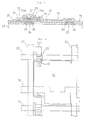
- Figure 1 is a partial sectional view of a substrate used in an embodiment of the invention.
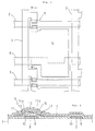
- Figure 2 is a plan view showing one portion of the substrate used in the embodiment.
- Figure 3 is a plan view showing one portion of a substrate used in a conventional display device.
- Figure 4 is a sectional view taken along line IV-IV of Fig. 3.
- FIG. 1 A preferred embodiment of the invention is shown in Figs. 1 and 2.
- Figure 2 is a partial plan view of a substrate used in the embodiment
- Fig. 1 is a sectional view taken along line I-I of Fig. 2.
- a plurality of gate bus lines 22 are formed in parallel and horizontally in Fig. 2, and a plurality of source bus lines 23 are formed vertically in the figure.
- a TFT 25 is formed in the vicinity of each intersection of the gate bus lines 22 and source bus lines 23, a TFT 25 is formed.
- Each TFT 25 drives a picture element electrode 24 which is disposed in each region surrounded by two adjacent gate bus lines 22 and two adjacent source bus lines 23.
- Under the picture element electrode 24, a capacitor electrode 26 is formed.
- a gate electrode 28 of the TFT 25 and a capacitor electrode 26 are formed on the surface of the insulating substrate 27, a gate electrode 28 of the TFT 25 and a capacitor electrode 26 are formed.
- the gate electrode 28 is one part of the gate bus line 22.
- the gate electrode 28 and capacitor electrode 26 can be formed simultaneously, and made of the same material.
- the above-mentioned parts of the structure of the preferred embodiment may be the same as those of the device of Fig. 3.
- An anodic oxidation film 29 is formed on each of the gate electrode 28 and capacitor electrode 26.
- a gate insulating layer 30 is formed on the anodic oxidation films 29 and the remaining surface of the insulating substrate 27.
- an i-a-Si film 31 and n+-a-Si films 33 are laminated on the gate insulating layer 30.
- the n+-a-Si films 33 are electrically separated by an SiN x insulating film 32 formed on the i-a-Si film 31.
- a source electrode 34a and a drain electrode 34b are formed on the n+-a-Si films 33, respectively.
- the source electrode 34a and drain electrode 34b are made of the same material as that of the source bus lines 23, and formed simultaneously with the source bus lines 23.
- the structure including the films 31, 32 and 33 and electrodes 28, 34a and 34b constitute the TFT 25.
- One end portion of the drain electrode 34b extends over the gate insulating layer 30.
- a protective insulating layer 35 is formed to cover the TFT 25 and the gate insulating layer 30.
- the picture element electrode 24 is formed on the protective insulating layer 35, and electrically connected to the drain electrode 34b through a contact hole 40 which is formed in the protective insulating layer 35.
- a three-layered dielectric laminated structure consisting of the anodic oxidation film 29, the gate insulating layer 30 and the protective insulating layer 35 is formed between the picture element electrode 24 and the capacitor electrode 26, so that an additional capacitor is formed by these two electrodes 24 and 26 and the three-layered dielectric laminated structure.
- the additional capacitor comprises the three-layered dielectric laminated structure, the insulation between the picture element electrode 24 and the capacitor electrode 26 will not easily fail as compared with that of the prior art which has a two-layered dielectric structure as mentioned above. Therefore, the possibility of producing electrical continuity between the picture element electrode 24 and the capacitor electrode 26 which is caused by a pinhole can be greatly reduced.
- a thin layer of a metal such as Ta, Al, or Ti is deposited in the thickness of 2000 - 4000 ⁇ by the sputtering or electron beam deposition technique.
- This thin metal film is patterned to form simultaneously the gate electrode 28 and the capacitor electrode 26.
- the surface of the gate electrode 28 and the capacitor electrode 26 is subjected to anodic oxidation to make the anodic oxidation film 29 thereon.
- the thickness of the anodic oxidation film 29 ranges from 1000 ⁇ to 3000 ⁇ .
- SiN x is deposited by a plasma CVD technique to form the gate insulating layer 30 (thickness: 2000 - 5000 ⁇ ), As a result, a two-layered dielectric lamination consisting of the anodic oxidation film 29 and the gate insulating layer 30 is formed.
- a semiconductor film of a-Si and an insulating film of SiN x are successively deposited, and then patterned by the photolithographic technique to form the a-Si film 31 and the SiN x insulating film 32.
- a semiconductor film of n+-a-Si is deposited, and then patterned by the photolithographic technique to form the n+-a-Si films 33.
- a metal such as Ti, Mo or W is deposited by the sputtering or electron beam deposition technique, and patterned by the Photolithographic technique to form the source electrode 34a and the drain electrode 34b.
- the protective insulating layer 35 made of SiN x is deposited in the thickness of 2000 - 6000 ⁇ by the plasma CVD technique, and the contact hole 40 is opened in the layer 35 by the photolithographic technique. Thereafter, a transparent conductive film which is mainly composed of indium oxide is deposited by the sputtering or electron beam deposition technique, and patterned to form the picture element electrode 24 which is electrically connected to the drain electrode 34b through the contact hole 40.
- the three-layered dielectric laminated structure which consists of the anodic oxidation film 29, the gate insulating layer 30 and the protective insulating layer 35 is disposed between the capacitor electrode 26 and the picture element electrode 24, thereby forming an additional capacitor.
- the protective insulating layer 35 may be made of another insulating material such as SiO2 in place of SiN x .
Landscapes
- Physics & Mathematics (AREA)
- Nonlinear Science (AREA)
- Engineering & Computer Science (AREA)
- Crystallography & Structural Chemistry (AREA)
- Mathematical Physics (AREA)
- Chemical & Material Sciences (AREA)
- Microelectronics & Electronic Packaging (AREA)
- Power Engineering (AREA)
- General Physics & Mathematics (AREA)
- Optics & Photonics (AREA)
- Liquid Crystal (AREA)
- Thin Film Transistor (AREA)
- Liquid Crystal Display Device Control (AREA)
- Devices For Indicating Variable Information By Combining Individual Elements (AREA)
Claims (5)
- Dispositif d'affichage à cristaux liquides du type à matrice active, qui comporte un substrat (27) et une matrice d'éléments d'affichage disposée sur ledit substrat (27), chaque élément d'affichage comprenant :
une électrode d'élément d'image (24) ;
un élément de commutation (25) situé à proximité de l'électrode d'élément d'image (24) et relié à l'électrode d'élément d'image (24) ;
une couche d'isolation protectrice (35) disposée par dessus l'élément de commutation (25) ;
une électrode de condensateur (26) placée face à une partie de l'électrode d'élément d'image (24), l'électrode de condensateur (26) et l'électrode d'élément d'image (24) formant un condensateur ; et
une structure diélectrique stratifiée disposée entre l'électrode de condensateur (26) et l'électrode d'élément d'image (24), la structure diélectrique stratifiée comprenant deux couches électriquement isolantes (29,30) ;
caractérisé en ce que :
ladite couche d'isolation protectrice (35) s'étend entre l'électrode d'élément d'image (24) et l'électrode de condensateur (26), pour ainsi former une couche d'isolation électrique supplémentaire entre l'électrode d'élément d'image (24) et l'électrode de condensateur (26). - Dispositif selon la revendication 1, dans lequel ledit élément de commutation est un transistor à couches minces (25), l'électrode de grille (28) dudit transistor à couches minces et ladite électrode de condensateur (26) sont disposées sur ledit substrat (27), et une couche d'isolation de grille (30) est formée à la fois sur ladite électrode de grille et sur ladite électrode de condensateur, ladite couche d'isolation de grille (30) étant l'une desdites deux couches isolantes.
- Dispositif selon la revendication 2, dans lequel un film d'oxydation anodique (29) est formé sur ladite électrode de condensateur (26), ledit film d'oxydation anodique (29) étant l'une desdites deux couches isolantes.
- Dispositif selon la revendication 1, 2 ou 3, dans lequel ladite électrode d'élément d'image (24) est disposée sur ladite couche d'isolation protectrice (35).
- Dispositif selon la revendication 2, 3 ou 4, dans lequel ladite électrode d'élément d'image (24) est reliée électriquement à l'électrode de drain dudit transistor à couches minces (25), au travers d'un trou de contact (40) qui est ménagé dans ladite couche d'isolation protectrice.
Applications Claiming Priority (2)
| Application Number | Priority Date | Filing Date | Title |
|---|---|---|---|
| JP200782/88 | 1988-08-10 | ||
| JP20078288A JPH0816756B2 (ja) | 1988-08-10 | 1988-08-10 | 透過型アクティブマトリクス液晶表示装置 |
Publications (3)
| Publication Number | Publication Date |
|---|---|
| EP0376437A2 EP0376437A2 (fr) | 1990-07-04 |
| EP0376437A3 EP0376437A3 (en) | 1990-10-31 |
| EP0376437B1 true EP0376437B1 (fr) | 1994-12-21 |
Family
ID=16430101
Family Applications (1)
| Application Number | Title | Priority Date | Filing Date |
|---|---|---|---|
| EP89308162A Expired - Lifetime EP0376437B1 (fr) | 1988-08-10 | 1989-08-10 | Dispositif d'affichage du type à matrice active à cristaux liquides |
Country Status (4)
| Country | Link |
|---|---|
| US (1) | US5054887A (fr) |
| EP (1) | EP0376437B1 (fr) |
| JP (1) | JPH0816756B2 (fr) |
| DE (1) | DE68920130T2 (fr) |
Families Citing this family (61)
| Publication number | Priority date | Publication date | Assignee | Title |
|---|---|---|---|---|
| JP2620240B2 (ja) * | 1987-06-10 | 1997-06-11 | 株式会社日立製作所 | 液晶表示装置 |
| US5231039A (en) * | 1988-02-25 | 1993-07-27 | Sharp Kabushiki Kaisha | Method of fabricating a liquid crystal display device |
| US5225364A (en) * | 1989-06-26 | 1993-07-06 | Oki Electric Industry Co., Ltd. | Method of fabricating a thin-film transistor matrix for an active matrix display panel |
| JP3009438B2 (ja) * | 1989-08-14 | 2000-02-14 | 株式会社日立製作所 | 液晶表示装置 |
| DE69117785T2 (de) * | 1990-03-27 | 1997-02-06 | Canon Kk | Dünnschicht-Halbleiterbauelement |
| FR2662290B1 (fr) * | 1990-05-15 | 1992-07-24 | France Telecom | Procede de realisation d'un ecran d'affichage a matrice active et a condensateurs de stockage et ecran obtenu par ce procede. |
| JP3226223B2 (ja) * | 1990-07-12 | 2001-11-05 | 株式会社東芝 | 薄膜トランジスタアレイ装置および液晶表示装置 |
| JPH0475034A (ja) * | 1990-07-17 | 1992-03-10 | Sharp Corp | アクティブマトリクス表示装置及びその製造方法 |
| US5153142A (en) * | 1990-09-04 | 1992-10-06 | Industrial Technology Research Institute | Method for fabricating an indium tin oxide electrode for a thin film transistor |
| US5402254B1 (en) * | 1990-10-17 | 1998-09-22 | Hitachi Ltd | Liquid crystal display device with tfts in which pixel electrodes are formed in the same plane as the gate electrodes with anodized oxide films before the deposition of silicon |
| JP3024661B2 (ja) * | 1990-11-09 | 2000-03-21 | セイコーエプソン株式会社 | アクティブマトリクス基板及びその製造方法 |
| US5206749A (en) | 1990-12-31 | 1993-04-27 | Kopin Corporation | Liquid crystal display having essentially single crystal transistors pixels and driving circuits |
| US5528397A (en) | 1991-12-03 | 1996-06-18 | Kopin Corporation | Single crystal silicon transistors for display panels |
| US5666175A (en) * | 1990-12-31 | 1997-09-09 | Kopin Corporation | Optical systems for displays |
| US5362671A (en) * | 1990-12-31 | 1994-11-08 | Kopin Corporation | Method of fabricating single crystal silicon arrayed devices for display panels |
| EP0499979A3 (en) | 1991-02-16 | 1993-06-09 | Semiconductor Energy Laboratory Co., Ltd. | Electro-optical device |
| JP2873632B2 (ja) * | 1991-03-15 | 1999-03-24 | 株式会社半導体エネルギー研究所 | 半導体装置 |
| US6713783B1 (en) | 1991-03-15 | 2004-03-30 | Semiconductor Energy Laboratory Co., Ltd. | Compensating electro-optical device including thin film transistors |
| JPH0572553A (ja) * | 1991-09-11 | 1993-03-26 | Hitachi Ltd | 液晶表示装置およびその製造方法 |
| US6979840B1 (en) * | 1991-09-25 | 2005-12-27 | Semiconductor Energy Laboratory Co., Ltd. | Thin film transistors having anodized metal film between the gate wiring and drain wiring |
| JP2907629B2 (ja) * | 1992-04-10 | 1999-06-21 | 松下電器産業株式会社 | 液晶表示パネル |
| JP3245959B2 (ja) * | 1992-06-05 | 2002-01-15 | 松下電器産業株式会社 | 液晶画像表示装置の製造方法 |
| JPH05341315A (ja) | 1992-06-08 | 1993-12-24 | Hitachi Ltd | 薄膜トランジスタ基板、液晶表示パネルおよび液晶表示装置 |
| US5707746A (en) * | 1992-09-25 | 1998-01-13 | Sharp Kabushiki Kaisha | Thin film transistor device with advanced characteristics by improved matching between a glass substrate and a silicon nitride layer |
| JP2924506B2 (ja) * | 1992-10-27 | 1999-07-26 | 日本電気株式会社 | アクティブマトリックス型液晶表示装置の画素構造 |
| WO1994013018A1 (fr) * | 1992-12-01 | 1994-06-09 | Litton Systems Canada Limited | Transistor a couches minces possedant un dielectrique de grille a trois couches, son procede de fabrication, et affichage a matrice active muni d'une pluralite de transistors de ce type |
| JP3098345B2 (ja) * | 1992-12-28 | 2000-10-16 | 富士通株式会社 | 薄膜トランジスタマトリクス装置及びその製造方法 |
| DE4339721C1 (de) * | 1993-11-22 | 1995-02-02 | Lueder Ernst | Verfahren zur Herstellung einer Matrix aus Dünnschichttransistoren |
| US5483366A (en) * | 1994-07-20 | 1996-01-09 | David Sarnoff Research Center Inc | LCD with hige capacitance pixel having an ITO active region/poly SI pixel region electrical connection and having poly SI selection line extensions along pixel edges |
| JPH08172202A (ja) * | 1994-12-20 | 1996-07-02 | Sharp Corp | 薄膜トランジスタおよびその製造方法 |
| JP2900229B2 (ja) | 1994-12-27 | 1999-06-02 | 株式会社半導体エネルギー研究所 | 半導体装置およびその作製方法および電気光学装置 |
| KR0145900B1 (ko) * | 1995-02-11 | 1998-09-15 | 김광호 | 박막 트랜지스터 액정디스플레이 소자 및 그 제조방법 |
| US5834327A (en) | 1995-03-18 | 1998-11-10 | Semiconductor Energy Laboratory Co., Ltd. | Method for producing display device |
| KR100303134B1 (ko) * | 1995-05-09 | 2002-11-23 | 엘지.필립스 엘시디 주식회사 | 액정표시소자및그제조방법. |
| FR2737314B1 (fr) * | 1995-07-28 | 1997-08-29 | Thomson Lcd | Procede de fabrication d'une matrice active pour ecran plat, ecran a cristaux liquides comportant une matrice active obtenue selon ledit procede et procede d'adressage d'un tel ecran |
| KR100205388B1 (ko) * | 1995-09-12 | 1999-07-01 | 구자홍 | 액정표시장치 및 그 제조방법 |
| JPH09236826A (ja) * | 1995-09-28 | 1997-09-09 | Sharp Corp | 液晶表示素子およびその製造方法 |
| EP0775931B1 (fr) | 1995-11-21 | 2005-10-05 | Samsung Electronics Co., Ltd. | Procédé de fabrication d'un afficheur à cristaux liquides |
| KR100190041B1 (ko) * | 1995-12-28 | 1999-06-01 | 윤종용 | 액정표시장치의 제조방법 |
| JP3205501B2 (ja) * | 1996-03-12 | 2001-09-04 | シャープ株式会社 | アクティブマトリクス表示装置およびその修正方法 |
| US6383899B1 (en) | 1996-04-05 | 2002-05-07 | Sharp Laboratories Of America, Inc. | Method of forming polycrystalline semiconductor film from amorphous deposit by modulating crystallization with a combination of pre-annealing and ion implantation |
| JPH1010583A (ja) * | 1996-04-22 | 1998-01-16 | Sharp Corp | アクティブマトリクス基板の製造方法、およびそのアクティブマトリクス基板 |
| KR100209620B1 (ko) * | 1996-08-31 | 1999-07-15 | 구자홍 | 액정 표시 장치 및 그 제조방법 |
| KR100241287B1 (ko) * | 1996-09-10 | 2000-02-01 | 구본준 | 액정표시소자 제조방법 |
| JPH10229197A (ja) * | 1997-02-17 | 1998-08-25 | Sanyo Electric Co Ltd | 薄膜トランジスタ、薄膜トランジスタの製造方法 |
| JP3376379B2 (ja) * | 1997-02-20 | 2003-02-10 | 富士通ディスプレイテクノロジーズ株式会社 | 液晶表示パネル、液晶表示装置及びその製造方法 |
| JP3592535B2 (ja) * | 1998-07-16 | 2004-11-24 | 株式会社半導体エネルギー研究所 | 半導体装置の作製方法 |
| US6124164A (en) * | 1998-09-17 | 2000-09-26 | Micron Technology, Inc. | Method of making integrated capacitor incorporating high K dielectric |
| JP2000275663A (ja) * | 1999-03-26 | 2000-10-06 | Hitachi Ltd | 液晶表示装置とその製造方法 |
| WO2001007961A1 (fr) * | 1999-07-21 | 2001-02-01 | E Ink Corporation | Utilisation d'un condensateur de memorisation pour ameliorer la performance d'un affichage electronique matriciel actif |
| KR100647775B1 (ko) * | 2004-12-01 | 2006-11-23 | 엘지.필립스 엘시디 주식회사 | 박막 트랜지스터 기판 및 제조 방법 |
| TWI257646B (en) * | 2005-09-05 | 2006-07-01 | Innolux Display Corp | Thin film transistor array substrate and method of manufacturing the same |
| CN101346751A (zh) | 2005-12-26 | 2009-01-14 | 夏普株式会社 | 有源矩阵基板、显示装置、电视接收机和有源矩阵基板的缺陷修正方法 |
| TWI304655B (en) * | 2006-04-07 | 2008-12-21 | Innolux Display Corp | Thin film transistor and method of manufacturing the same |
| CN100529866C (zh) * | 2006-04-19 | 2009-08-19 | 群康科技(深圳)有限公司 | 液晶显示器制造方法 |
| TWI339303B (en) * | 2006-12-15 | 2011-03-21 | Chimei Innolux Corp | Liquid crystal panel |
| JP5182993B2 (ja) | 2008-03-31 | 2013-04-17 | 株式会社半導体エネルギー研究所 | 表示装置及びその作製方法 |
| KR101804589B1 (ko) * | 2009-12-11 | 2018-01-10 | 가부시키가이샤 한도오따이 에네루기 켄큐쇼 | 반도체 장치 및 그 제조 방법 |
| JP5735255B2 (ja) | 2010-10-28 | 2015-06-17 | 株式会社ハイレックスコーポレーション | 係留装置及びそれを用いたステアリング係留機構 |
| TWI422940B (zh) * | 2010-12-16 | 2014-01-11 | Innolux Corp | 陣列基板的形成方法 |
| CN110797353A (zh) * | 2019-11-12 | 2020-02-14 | 京东方科技集团股份有限公司 | 阵列基板、显示面板和显示装置 |
Family Cites Families (9)
| Publication number | Priority date | Publication date | Assignee | Title |
|---|---|---|---|---|
| US3671820A (en) * | 1970-04-27 | 1972-06-20 | Rudolph R Haering | High voltage thin-film transistor |
| JPS5922029A (ja) * | 1982-07-28 | 1984-02-04 | Matsushita Electric Ind Co Ltd | マトリクス表示パネルの製造方法 |
| JPS6045219A (ja) * | 1983-08-23 | 1985-03-11 | Toshiba Corp | アクテイブマトリクス型表示装置 |
| GB2169746B (en) * | 1984-11-13 | 1988-09-14 | Sharp Kk | Thin film transistor |
| US4571816A (en) * | 1984-12-11 | 1986-02-25 | Rca Corporation | Method of making a capacitor with standard self-aligned gate process |
| JPS62285464A (ja) * | 1986-06-03 | 1987-12-11 | Matsushita Electric Ind Co Ltd | 薄膜トランジスタアレイ基板及びその製造方法 |
| US4955697A (en) * | 1987-04-20 | 1990-09-11 | Hitachi, Ltd. | Liquid crystal display device and method of driving the same |
| JPH01291467A (ja) * | 1988-05-19 | 1989-11-24 | Toshiba Corp | 薄膜トランジスタ |
| JP3351026B2 (ja) * | 1993-06-04 | 2002-11-25 | 松下電器産業株式会社 | 電気湯沸かし器 |
-
1988
- 1988-08-10 JP JP20078288A patent/JPH0816756B2/ja not_active Expired - Lifetime
-
1989
- 1989-08-09 US US07/391,244 patent/US5054887A/en not_active Expired - Lifetime
- 1989-08-10 DE DE68920130T patent/DE68920130T2/de not_active Expired - Fee Related
- 1989-08-10 EP EP89308162A patent/EP0376437B1/fr not_active Expired - Lifetime
Also Published As
| Publication number | Publication date |
|---|---|
| DE68920130T2 (de) | 1995-06-22 |
| DE68920130D1 (de) | 1995-02-02 |
| JPH0816756B2 (ja) | 1996-02-21 |
| US5054887A (en) | 1991-10-08 |
| EP0376437A3 (en) | 1990-10-31 |
| JPH0248639A (ja) | 1990-02-19 |
| EP0376437A2 (fr) | 1990-07-04 |
Similar Documents
| Publication | Publication Date | Title |
|---|---|---|
| US5054887A (en) | Active matrix type liquid crystal display | |
| US4935792A (en) | Thin film transistor array | |
| US4759610A (en) | Active matrix display with capacitive light shield | |
| US5504348A (en) | Thin-film transistor array and liquid crystal display device using the thin-film transistor array | |
| US5162901A (en) | Active-matrix display device with added capacitance electrode wire and secondary wire connected thereto | |
| EP0301571B1 (fr) | Matrice de transistors en couche mince | |
| US5231039A (en) | Method of fabricating a liquid crystal display device | |
| KR100260359B1 (ko) | 액정 표시 장치 및 그 제조방법 | |
| EP0329887B1 (fr) | Dispositif d'affichage à cristaux liquides | |
| US5017984A (en) | Amorphous silicon thin film transistor array | |
| GB2197985A (en) | Liquid crystal display | |
| US5734448A (en) | LCD having a capacitor with two lower capacitor electrodes and a reflective pixel electrode serving as an upper electrode | |
| US5155564A (en) | Thin-film transistor array | |
| US5623350A (en) | Liquid crystal display with supplemental capacitors and method for manufacturing the same | |
| JPH07113728B2 (ja) | アクティブマトリクス基板 | |
| US5103330A (en) | Matrix-type liquid-crystal display panel having redundant conductor structures | |
| US5270845A (en) | Liquid crystal display unit manufacturing method including forming one of two gate line layers of display electrode material | |
| JP3167817B2 (ja) | アクティブマトリックス型液晶表示装置 | |
| JPH0444014A (ja) | アクティブマトリクス型液晶表示装置 | |
| JP3059783B2 (ja) | 液晶表示装置 | |
| JPH0340511B2 (fr) | ||
| JP2538523B2 (ja) | 液晶マトリクスパネルの製造方法 | |
| JPH03153217A (ja) | Tftパネルおよびその製造方法 | |
| JP2664814B2 (ja) | アクティブマトリクス表示装置 | |
| JP2932826B2 (ja) | 表示装置 |
Legal Events
| Date | Code | Title | Description |
|---|---|---|---|
| PUAI | Public reference made under article 153(3) epc to a published international application that has entered the european phase |
Free format text: ORIGINAL CODE: 0009012 |
|
| AK | Designated contracting states |
Kind code of ref document: A2 Designated state(s): DE FR GB NL |
|
| PUAL | Search report despatched |
Free format text: ORIGINAL CODE: 0009013 |
|
| AK | Designated contracting states |
Kind code of ref document: A3 Designated state(s): DE FR GB NL |
|
| 17P | Request for examination filed |
Effective date: 19901228 |
|
| 17Q | First examination report despatched |
Effective date: 19930303 |
|
| GRAA | (expected) grant |
Free format text: ORIGINAL CODE: 0009210 |
|
| AK | Designated contracting states |
Kind code of ref document: B1 Designated state(s): DE FR GB NL |
|
| REF | Corresponds to: |
Ref document number: 68920130 Country of ref document: DE Date of ref document: 19950202 |
|
| ET | Fr: translation filed | ||
| PLBE | No opposition filed within time limit |
Free format text: ORIGINAL CODE: 0009261 |
|
| STAA | Information on the status of an ep patent application or granted ep patent |
Free format text: STATUS: NO OPPOSITION FILED WITHIN TIME LIMIT |
|
| 26N | No opposition filed | ||
| PGFP | Annual fee paid to national office [announced via postgrant information from national office to epo] |
Ref country code: DE Payment date: 20010806 Year of fee payment: 13 |
|
| PGFP | Annual fee paid to national office [announced via postgrant information from national office to epo] |
Ref country code: GB Payment date: 20010808 Year of fee payment: 13 |
|
| PGFP | Annual fee paid to national office [announced via postgrant information from national office to epo] |
Ref country code: FR Payment date: 20010810 Year of fee payment: 13 |
|
| PGFP | Annual fee paid to national office [announced via postgrant information from national office to epo] |
Ref country code: NL Payment date: 20010830 Year of fee payment: 13 |
|
| REG | Reference to a national code |
Ref country code: GB Ref legal event code: IF02 |
|
| PG25 | Lapsed in a contracting state [announced via postgrant information from national office to epo] |
Ref country code: GB Free format text: LAPSE BECAUSE OF NON-PAYMENT OF DUE FEES Effective date: 20020810 |
|
| PG25 | Lapsed in a contracting state [announced via postgrant information from national office to epo] |
Ref country code: NL Free format text: LAPSE BECAUSE OF NON-PAYMENT OF DUE FEES Effective date: 20030301 Ref country code: DE Free format text: LAPSE BECAUSE OF NON-PAYMENT OF DUE FEES Effective date: 20030301 |
|
| GBPC | Gb: european patent ceased through non-payment of renewal fee |
Effective date: 20020810 |
|
| PG25 | Lapsed in a contracting state [announced via postgrant information from national office to epo] |
Ref country code: FR Free format text: LAPSE BECAUSE OF NON-PAYMENT OF DUE FEES Effective date: 20030430 |
|
| NLV4 | Nl: lapsed or anulled due to non-payment of the annual fee |
Effective date: 20030301 |
|
| REG | Reference to a national code |
Ref country code: FR Ref legal event code: ST |