EP0468901A1 - Verfahren zur Herstellung eines EPROM-Speichers mit unterschiedlichen Source- und Drain-Strukturen - Google Patents
Verfahren zur Herstellung eines EPROM-Speichers mit unterschiedlichen Source- und Drain-Strukturen Download PDFInfo
- Publication number
- EP0468901A1 EP0468901A1 EP91420266A EP91420266A EP0468901A1 EP 0468901 A1 EP0468901 A1 EP 0468901A1 EP 91420266 A EP91420266 A EP 91420266A EP 91420266 A EP91420266 A EP 91420266A EP 0468901 A1 EP0468901 A1 EP 0468901A1
- Authority
- EP
- European Patent Office
- Prior art keywords
- layer
- drain
- grid
- sources
- etching
- Prior art date
- Legal status (The legal status is an assumption and is not a legal conclusion. Google has not performed a legal analysis and makes no representation as to the accuracy of the status listed.)
- Granted
Links
Images



Classifications
-
- H—ELECTRICITY
- H10—SEMICONDUCTOR DEVICES; ELECTRIC SOLID-STATE DEVICES NOT OTHERWISE PROVIDED FOR
- H10B—ELECTRONIC MEMORY DEVICES
- H10B69/00—Erasable-and-programmable ROM [EPROM] devices not provided for in groups H10B41/00 - H10B63/00, e.g. ultraviolet erasable-and-programmable ROM [UVEPROM] devices
-
- H—ELECTRICITY
- H10—SEMICONDUCTOR DEVICES; ELECTRIC SOLID-STATE DEVICES NOT OTHERWISE PROVIDED FOR
- H10B—ELECTRONIC MEMORY DEVICES
- H10B41/00—Electrically erasable-and-programmable ROM [EEPROM] devices comprising floating gates
- H10B41/30—Electrically erasable-and-programmable ROM [EEPROM] devices comprising floating gates characterised by the memory core region
Definitions
- the present invention relates to semiconductor memories and more particularly to floating gate memories, non-volatile and electrically programmable, commonly called EPROM memories.
- FIG. 1A represents a transistor T of a floating gate memory point.
- This transistor has a floating gate 1 and a control gate 2, as well as two semiconductor regions of a first conductivity type (source 3 and drain 4) separated by a channel region of an opposite conductivity type covered by the gate. floating 1 and the control grid 2.
- the control gate 2 is connected to a word line LM.
- the drain 4 is connected to a bit line LB.
- Source 3 is connected to ground.
- the floating gate 1 is charged by injection of hot carriers, by applying to the control gate 2, while the transistor conducts a current between its source 3 and drain 4 regions, a sufficiently high potential for the charge carriers (electrons) to be attracted and trapped in the floating grid.
- This writing operation has the effect of increasing the conduction threshold of the transistor which, once programmed, will conduct the current only for potential values applied to its control gate higher than in the absence of programming.
- a voltage is applied to the control gate of the transistor of this memory point that is both higher than the conduction trigger threshold voltage in the non-programmed state and lower than the conduction trigger threshold voltage in the programmed state. If the transistor conducts when a suitable potential difference is applied between the source and the drain, the memory point is in the non-programmed state. If the transistor does not drive, the memory point is in the programmed state.
- VPP programming potential The potential applied to the control grid when programming the memory point, or VPP programming potential, is for example 15 volts.
- the drain potential VCC is then for example 10 volts and the source potential VSS is for example 0 volts or ground.
- the potential applied to the control grid when reading the memory point is for example 5 volts.
- the drain potential VCC is then for example 1.5 volts, and the source potential VSS is for example 0 volts or ground.
- FIG. 1B represents a sectional view of a memory point implanted in a silicon wafer.
- the transistor comprises a floating gate 1, a control gate 2, a source region 3 is a drain region 4.
- the source and the drain are two semiconductor regions of a first type of conductivity, for example N+, separated by a channel region 7 of an opposite type of conductivity, for example P-.
- the floating gate 1 of the transistor is produced by a first level of polycrystalline silicon (poly 1). It is separated from the substrate by a thin layer of silicon dioxide 5, called the gate oxide layer. A layer of silicon dioxide 6 is present between the layers of grids 1 and 2. The control grid 2 is produced by a second level of polycrystalline silicon (poly 2). The silicon dioxide layer 6 is called the interpoly oxide layer.
- One of the problems for producing EPROM memories comprising a large number of cells of the type illustrated very diagrammatically in FIG. 1B is to ensure with the minimum loss of surface the connection between all the drains of the cells of the same column (drain or bit line) and between all the control grids of the same row (word line), while connecting all sources to ground.
- bit lines (drains) and the ground lines (sources) are clearly differentiated.
- the conductive layer is made of a refractory metal and the metallization steps include contact resumption with aluminum.
- FIG. 2 is a symbolic and extremely schematic top view of a set of memory cells. It is only intended to facilitate the understanding of the memory topology.
- the source, gate and drain regions of an elementary transistor have been designated by S, G, D. Each of these transistors is oriented in the direction of the columns in the representation of FIG. 2. Thus, vertically, there is successively a source region S (N+ diffusion), a grid region G (floating grid and control grid) then a drain region D (diffusion N+) and again a gate region and a source region, and so on.
- the dotted zones designate zones of thick oxide or field oxide separating columns of adjacent transistors except at the locations of the sources.
- the N+ source diffusions are continuous in rows while the drain diffusions are in the form of isolated islands.
- All the control grids of the same row are interconnected as will be seen below by a word line LM corresponding to a second level of polycrystalline silicon and to silicide.
- bit line LB made of a refractory metal formed above the second level of polycrystalline silicon.
- a memory can be produced according to the present invention by horizontally repeating groups of 16 elementary cells separated by a source recovery column such as column 10 in FIG. 2 and, vertically, one can find more than 1000 transistors per column. It will also be noted hereinafter that the present invention makes it possible to minimize the number of repeats of drain contact on the aforementioned refractory, possibly with a single contact every 1000 transistors.
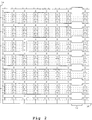
- Figure 3 shows a top view of a memory portion according to the present invention in an intermediate manufacturing step (corresponding to that of Figures 4 and 5A which will be described below).
- the brace 14 designates the limits of a thick oxide column formed between two columns of transistors and the brace 15, the limits of a thick oxide column framing the zone 10 which will be used for source contact recovery.
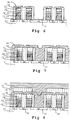
- FIG. 4 represents a sectional view along line AA of FIG. 3 at an intermediate manufacturing stage when only the thick oxide zones have been formed and that all of the successive layers have been deposited and etched in a conventional manner intended to form the floating and control grids.
- a monocrystalline silicon substrate 21 a first layer of gate oxide 22, a first level of polycrystalline silicon (poly 1) 23 corresponding to the floating gates, a layer of thin oxide 24 ( layer of interpoly oxide), a second level of polycrystalline silicon (poly 2) 25 corresponding to the control grids, a layer of a refractory metal silicide 26, a layer of thick silicon oxide 27, a third level of silicon polycrystalline 28 and a resin layer 29.
- the resin mask 29 has been etched according to a pattern chosen to delimit source regions 31 and 32 and a central drain region 33. (We also find drain regions outside the source regions 31 and 32).
- the drain region 33 is wider than the source regions 31 and 32, for reasons which will appear below.
- FIGS. 5A and 5B represent views in section in the same direction as FIG. 4, but along the line BB of FIG. 3. This section, instead of being located in the middle of a column of transistor, is located slightly at the distance of this column in a region where field oxide is present, 35.
- FIG. 5A represents the state of the structure while the grid layers 22 to 29 have been etched but before carrying out the drain and source implantations.
- the etching of the grid layers extends to the thick oxide layer 35.
- a resin layer 37 masks the drain regions. Then, as shown in FIG. 5B, the thick oxide layer 35 is etched at the sources, and the source diffusions 31 and 32 are carried out at the same time as the drain diffusion 33 illustrated in FIG. 4. The structure of FIG. 5B is also shown after removal of the upper resin layers 29 and 37.
- FIGS. 6 to 8 represent sections A-A at successive stages of manufacture subsequent to those illustrated in FIGS. 4 and 5.
- an oxide layer 40 is deposited chemically in the vapor phase so as to fill the relatively narrow intervals between the grid patterns situated on either side of a source region and to form spacers on the vertical walls of the grid patterns on either side of a drain pattern. Indeed, as we have seen previously, the drain regions are significantly wider than the source regions (with the exception of the source contact recovery regions).
- a vertical anisotropic attack was carried out on the oxide layer 40 in order to remove it above the silicon surfaces and more particularly above the doped drain region N+ 33 .
- the silicon layer 28 (third level of polycrystalline silicon) is used to stop the etching above the stack of grid layers. After which, this layer 28 is oxidized (at the same time as the visible part of the drain region 33 is oxidized, this visible part nonetheless oxidizes less quickly owing to the fact that it is mono silicon and not polycrystalline).
- the third level layer of polycrystalline silicon having a thin and well determined thickness, its oxidation and then the removal of the oxide layer formed simultaneously on the drain region 33 is done by consuming a relatively well determined oxide thickness.
- the thickness of the remaining oxide region 27 can be precisely determined. This constitutes an important advantage compared to the structures of the prior art, in which this thickness is poorly determined following the various stages of oxidation and etching of oxide. This thickness, although not critical, must be as small as possible to allow an acceleration of the manufacturing process while being high enough to maintain at a reasonable value, and preferably known, the parasitic capacities between the control grids and the metallizations then filed.
- planarization oxide 42 deposits a layer of planarization oxide 42, then a layer of a contact recovery metal 43, for example aluminum.
- a contact recovery metal 43 for example aluminum.
- FIG. 8 an opening is shown in the planarization oxide layer 42 and a contact between the aluminum layer 43 and the tungsten layer 41.
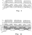
- FIG. 9 represents a sectional view along line CC of FIG. 3, that is to say perpendicular to drain regions. This figure shows the regions of diffusion of drain 33, of field oxide 35, of metallization of drain 41, isolation 42 and metallization 43. In the case of FIG. 9, a situation has been shown where the cut is made outside of contact regions between the metallizations 43 and the drain metallizations 41.
- FIG. 10 represents a sectional view along line D-D of FIG. 3, that is to say at the level of the grids of the memory cells.
- This figure is self-explanatory from the previous description. We have only reported the references corresponding to those of the previous figures. It will be noted that the connection of control grid to control grid in a row is made by the whole of the second level of polycrystalline silicon 25 and of refractory metal silicide 26. It is therefore a high conductivity bond which directly constitutes a word line.
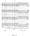
- FIG. 11 represents a top view similar to that of FIG. 3 but in the context of a particular embodiment in which there are shown in addition, by rectangles, repeats in which there is shown in plus, by rectangles, drain contact resumption and source contact resumption, that is to say, with regard to drains, contact between the tungsten layer 41 and the upper aluminum layer and, with regard to the sources, a contact between the upper aluminum layer and the source tungsten layer which is widened, as indicated in relation to FIG. 2, once every sixteen cells. Since it is not necessary to resume contact with each source recovery region and each drain region, it is possible, as shown, to widen the contact zones, which simplifies the process of manufacturing.
- insulation layers have been mentioned simply as being silicon oxide (SiO2) layers. Those skilled in the art will know how to choose other insulators or a combination of insulators for some of these layers, for example oxide-nitride-silicon oxide (ONO) sandwiches. Other insulating layers may be doped so as to promote their creep properties.
- various variants may be made to the method of the invention. For example, the deposition step of the polycrystalline silicon layer 28 can be omitted provided that controlled operations of partial etching of silicon oxide are then carried out.
- a step can be obtained in the direction of the lines of 1.5 micrometers and in the direction of the columns of 1.15 micrometers, which corresponds to a memory point area of 1.725 square micrometers.
Landscapes
- Semiconductor Memories (AREA)
- Non-Volatile Memory (AREA)
- Semiconductor Integrated Circuits (AREA)
Applications Claiming Priority (2)
| Application Number | Priority Date | Filing Date | Title |
|---|---|---|---|
| FR9009718 | 1990-07-24 | ||
| FR9009718A FR2665301A1 (fr) | 1990-07-24 | 1990-07-24 | Memoire eprom a drain et source de structures differentes. |
Publications (2)
| Publication Number | Publication Date |
|---|---|
| EP0468901A1 true EP0468901A1 (de) | 1992-01-29 |
| EP0468901B1 EP0468901B1 (de) | 1996-01-03 |
Family
ID=9399240
Family Applications (1)
| Application Number | Title | Priority Date | Filing Date |
|---|---|---|---|
| EP91420266A Expired - Lifetime EP0468901B1 (de) | 1990-07-24 | 1991-07-22 | Verfahren zur Herstellung eines EPROM-Speichers mit unterschiedlichen Source- und Drain-Strukturen |
Country Status (4)
| Country | Link |
|---|---|
| EP (1) | EP0468901B1 (de) |
| JP (1) | JPH04233767A (de) |
| DE (1) | DE69116022T2 (de) |
| FR (1) | FR2665301A1 (de) |
Cited By (2)
| Publication number | Priority date | Publication date | Assignee | Title |
|---|---|---|---|---|
| FR2711275A1 (fr) * | 1993-10-15 | 1995-04-21 | Intel Corp | Procédé automatiquement aligné de contact en fabrication de semi-conducteurs et dispositifs produits. |
| WO1995017010A1 (en) * | 1993-12-16 | 1995-06-22 | National Semiconductor Corporation | An increased-density flash eprom that requires less area to form the metal bit line-to-drain contacts |
Families Citing this family (1)
| Publication number | Priority date | Publication date | Assignee | Title |
|---|---|---|---|---|
| KR100500448B1 (ko) | 2003-02-06 | 2005-07-14 | 삼성전자주식회사 | 선택적 디스포저블 스페이서 기술을 사용하는 반도체집적회로의 제조방법 및 그에 의해 제조된 반도체 집적회로 |
Citations (2)
| Publication number | Priority date | Publication date | Assignee | Title |
|---|---|---|---|---|
| US4829351A (en) * | 1987-03-16 | 1989-05-09 | Motorola, Inc. | Polysilicon pattern for a floating gate memory |
| EP0368097A2 (de) * | 1988-11-10 | 1990-05-16 | Texas Instruments Incorporated | In den Kreuzungspunkten einer Matrix kontaklos angeordnete Speicher mit schwebendem Gate und eingebetteten Silicid-Bitleitungen |
-
1990
- 1990-07-24 FR FR9009718A patent/FR2665301A1/fr active Pending
-
1991
- 1991-07-22 EP EP91420266A patent/EP0468901B1/de not_active Expired - Lifetime
- 1991-07-22 DE DE69116022T patent/DE69116022T2/de not_active Expired - Fee Related
- 1991-07-24 JP JP3206138A patent/JPH04233767A/ja active Pending
Patent Citations (2)
| Publication number | Priority date | Publication date | Assignee | Title |
|---|---|---|---|---|
| US4829351A (en) * | 1987-03-16 | 1989-05-09 | Motorola, Inc. | Polysilicon pattern for a floating gate memory |
| EP0368097A2 (de) * | 1988-11-10 | 1990-05-16 | Texas Instruments Incorporated | In den Kreuzungspunkten einer Matrix kontaklos angeordnete Speicher mit schwebendem Gate und eingebetteten Silicid-Bitleitungen |
Cited By (3)
| Publication number | Priority date | Publication date | Assignee | Title |
|---|---|---|---|---|
| FR2711275A1 (fr) * | 1993-10-15 | 1995-04-21 | Intel Corp | Procédé automatiquement aligné de contact en fabrication de semi-conducteurs et dispositifs produits. |
| US5731242A (en) * | 1993-10-15 | 1998-03-24 | Intel Corporation | Self-aligned contact process in semiconductor fabrication |
| WO1995017010A1 (en) * | 1993-12-16 | 1995-06-22 | National Semiconductor Corporation | An increased-density flash eprom that requires less area to form the metal bit line-to-drain contacts |
Also Published As
| Publication number | Publication date |
|---|---|
| FR2665301A1 (fr) | 1992-01-31 |
| DE69116022D1 (de) | 1996-02-15 |
| JPH04233767A (ja) | 1992-08-21 |
| EP0468901B1 (de) | 1996-01-03 |
| DE69116022T2 (de) | 1996-09-05 |
Similar Documents
| Publication | Publication Date | Title |
|---|---|---|
| EP0258141B1 (de) | MIS integrierte Schaltung, wie eine EPROM-Speicherzelle, und Verfahren zu deren Herstellung | |
| EP0299853B1 (de) | Verfahren zum Herstellen einer Speicherzelle | |
| EP0648375B1 (de) | Flash-eeprom-speicher mit drei gateelektroden und sein herstellungsverfahren. | |
| FR2933802A1 (fr) | Structure et procede de realisation d'un dispositif microelectronique de memoire 3d de type flash nand. | |
| EP0712163A1 (de) | Elektrisch löschbares nicht-flüchtiges Speicherbauteil und Verfahren zur Herstellung desselben | |
| EP1292984A1 (de) | Elektronisches speicherbauelement in damaszenstruktur und dessen herstellungsverfahren | |
| FR3030883A1 (fr) | Cellule memoire a grille de selection verticale formee dans un substrat de type fdsoi | |
| EP0351316A1 (de) | Verfahren zur Herstellung einer integrierten Speicher-Zelle | |
| EP4075504A1 (de) | Programmierbare und löschbare speicherzelle | |
| FR3003691A1 (fr) | Finfet avec grille arriere | |
| EP3843158B1 (de) | Vorrichtung umfassend transistoren mit rundum-gate und herstellungsverfahren einer solchen vorrichtung | |
| EP0282520B1 (de) | Nichtflüchtiger speicher mit isoliertem gate ohne dickes oxid | |
| EP0354858B1 (de) | Hochintegrierte EPROM-Speicheranordnung mit einem grossen Kopplungsfaktor | |
| EP0468901B1 (de) | Verfahren zur Herstellung eines EPROM-Speichers mit unterschiedlichen Source- und Drain-Strukturen | |
| EP2286450B1 (de) | Schreibgeschützter speicher mit eeprom-struktur | |
| EP3843143B1 (de) | 3d-speicher und dessen herstellungsverfahren | |
| EP0379449A1 (de) | Verfahren zur Herstellung von integrierten Schaltungen | |
| FR2830124A1 (fr) | Memoire vive | |
| EP1677347B1 (de) | Magnetischer Speicher | |
| EP1586118B1 (de) | Vergrabener kondensator für eine sram-speicherzelle | |
| EP1094510A1 (de) | Herstellungsverfahren von EEPROM-Speicherstellen | |
| FR3155116A1 (fr) | circuit intégré comportant une cellule mémoire et procédé de fabrication correspondant | |
| FR3144402A1 (fr) | Circuit électronique comprenant une cellule de transistors | |
| FR3164829A1 (fr) | Réduction de la consommation d’énergie de programmation ou d’effacement d’une cellule mémoire à grille divisée, cellule mémoire et procédé de fabrication | |
| EP4429436A1 (de) | Verfahren zur herstellung eines elektronischen chips mit einer speicherschaltung |
Legal Events
| Date | Code | Title | Description |
|---|---|---|---|
| PUAI | Public reference made under article 153(3) epc to a published international application that has entered the european phase |
Free format text: ORIGINAL CODE: 0009012 |
|
| AK | Designated contracting states |
Kind code of ref document: A1 Designated state(s): DE FR GB IT |
|
| 17P | Request for examination filed |
Effective date: 19920703 |
|
| 17Q | First examination report despatched |
Effective date: 19940831 |
|
| GRAA | (expected) grant |
Free format text: ORIGINAL CODE: 0009210 |
|
| AK | Designated contracting states |
Kind code of ref document: B1 Designated state(s): DE FR GB IT |
|
| REF | Corresponds to: |
Ref document number: 69116022 Country of ref document: DE Date of ref document: 19960215 |
|
| ITF | It: translation for a ep patent filed | ||
| GBT | Gb: translation of ep patent filed (gb section 77(6)(a)/1977) |
Effective date: 19960219 |
|
| PLBE | No opposition filed within time limit |
Free format text: ORIGINAL CODE: 0009261 |
|
| STAA | Information on the status of an ep patent application or granted ep patent |
Free format text: STATUS: NO OPPOSITION FILED WITHIN TIME LIMIT |
|
| 26N | No opposition filed | ||
| PGFP | Annual fee paid to national office [announced via postgrant information from national office to epo] |
Ref country code: FR Payment date: 20000711 Year of fee payment: 10 |
|
| PGFP | Annual fee paid to national office [announced via postgrant information from national office to epo] |
Ref country code: DE Payment date: 20000717 Year of fee payment: 10 |
|
| PGFP | Annual fee paid to national office [announced via postgrant information from national office to epo] |
Ref country code: GB Payment date: 20000719 Year of fee payment: 10 |
|
| PG25 | Lapsed in a contracting state [announced via postgrant information from national office to epo] |
Ref country code: GB Free format text: LAPSE BECAUSE OF NON-PAYMENT OF DUE FEES Effective date: 20010722 |
|
| GBPC | Gb: european patent ceased through non-payment of renewal fee |
Effective date: 20010722 |
|
| PG25 | Lapsed in a contracting state [announced via postgrant information from national office to epo] |
Ref country code: FR Free format text: LAPSE BECAUSE OF NON-PAYMENT OF DUE FEES Effective date: 20020329 |
|
| PG25 | Lapsed in a contracting state [announced via postgrant information from national office to epo] |
Ref country code: DE Free format text: LAPSE BECAUSE OF NON-PAYMENT OF DUE FEES Effective date: 20020501 |
|
| REG | Reference to a national code |
Ref country code: FR Ref legal event code: ST |
|
| PG25 | Lapsed in a contracting state [announced via postgrant information from national office to epo] |
Ref country code: IT Free format text: LAPSE BECAUSE OF NON-PAYMENT OF DUE FEES;WARNING: LAPSES OF ITALIAN PATENTS WITH EFFECTIVE DATE BEFORE 2007 MAY HAVE OCCURRED AT ANY TIME BEFORE 2007. THE CORRECT EFFECTIVE DATE MAY BE DIFFERENT FROM THE ONE RECORDED. Effective date: 20050722 |