EP0475666B1 - Verfahren zur Herstellung einer Solarzelle aus amorphem Silizium - Google Patents
Verfahren zur Herstellung einer Solarzelle aus amorphem Silizium Download PDFInfo
- Publication number
- EP0475666B1 EP0475666B1 EP91308087A EP91308087A EP0475666B1 EP 0475666 B1 EP0475666 B1 EP 0475666B1 EP 91308087 A EP91308087 A EP 91308087A EP 91308087 A EP91308087 A EP 91308087A EP 0475666 B1 EP0475666 B1 EP 0475666B1
- Authority
- EP
- European Patent Office
- Prior art keywords
- film
- dehydrohalogenation
- solar cell
- silicon
- amorphous silicon
- Prior art date
- Legal status (The legal status is an assumption and is not a legal conclusion. Google has not performed a legal analysis and makes no representation as to the accuracy of the status listed.)
- Expired - Lifetime
Links
Images

Classifications
-
- H—ELECTRICITY
- H10—SEMICONDUCTOR DEVICES; ELECTRIC SOLID-STATE DEVICES NOT OTHERWISE PROVIDED FOR
- H10F—INORGANIC SEMICONDUCTOR DEVICES SENSITIVE TO INFRARED RADIATION, LIGHT, ELECTROMAGNETIC RADIATION OF SHORTER WAVELENGTH OR CORPUSCULAR RADIATION
- H10F10/00—Individual photovoltaic cells, e.g. solar cells
- H10F10/10—Individual photovoltaic cells, e.g. solar cells having potential barriers
- H10F10/17—Photovoltaic cells having only PIN junction potential barriers
-
- H—ELECTRICITY
- H10—SEMICONDUCTOR DEVICES; ELECTRIC SOLID-STATE DEVICES NOT OTHERWISE PROVIDED FOR
- H10F—INORGANIC SEMICONDUCTOR DEVICES SENSITIVE TO INFRARED RADIATION, LIGHT, ELECTROMAGNETIC RADIATION OF SHORTER WAVELENGTH OR CORPUSCULAR RADIATION
- H10F71/00—Manufacture or treatment of devices covered by this subclass
- H10F71/10—Manufacture or treatment of devices covered by this subclass the devices comprising amorphous semiconductor material
- H10F71/103—Manufacture or treatment of devices covered by this subclass the devices comprising amorphous semiconductor material including only Group IV materials
-
- Y—GENERAL TAGGING OF NEW TECHNOLOGICAL DEVELOPMENTS; GENERAL TAGGING OF CROSS-SECTIONAL TECHNOLOGIES SPANNING OVER SEVERAL SECTIONS OF THE IPC; TECHNICAL SUBJECTS COVERED BY FORMER USPC CROSS-REFERENCE ART COLLECTIONS [XRACs] AND DIGESTS
- Y02—TECHNOLOGIES OR APPLICATIONS FOR MITIGATION OR ADAPTATION AGAINST CLIMATE CHANGE
- Y02E—REDUCTION OF GREENHOUSE GAS [GHG] EMISSIONS, RELATED TO ENERGY GENERATION, TRANSMISSION OR DISTRIBUTION
- Y02E10/00—Energy generation through renewable energy sources
- Y02E10/50—Photovoltaic [PV] energy
- Y02E10/548—Amorphous silicon PV cells
-
- Y—GENERAL TAGGING OF NEW TECHNOLOGICAL DEVELOPMENTS; GENERAL TAGGING OF CROSS-SECTIONAL TECHNOLOGIES SPANNING OVER SEVERAL SECTIONS OF THE IPC; TECHNICAL SUBJECTS COVERED BY FORMER USPC CROSS-REFERENCE ART COLLECTIONS [XRACs] AND DIGESTS
- Y02—TECHNOLOGIES OR APPLICATIONS FOR MITIGATION OR ADAPTATION AGAINST CLIMATE CHANGE
- Y02P—CLIMATE CHANGE MITIGATION TECHNOLOGIES IN THE PRODUCTION OR PROCESSING OF GOODS
- Y02P70/00—Climate change mitigation technologies in the production process for final industrial or consumer products
- Y02P70/50—Manufacturing or production processes characterised by the final manufactured product
Definitions
- the present invention relates to an amorphous silicon solar cell, and more specifically, it relates to a manufacturing technique of an amorphous silicon solar cell stably having excellent photovoltaic characteristics.
- amorphous silicon solar cell has already been put into practice as a small-output energy feed source for driving portable a calculator and a watch.
- the amorphous silicon solar cell is not sufficient in points of performance and stability as an energy feed source having a large output of 0.1 W or more which can be utilized to generate electricity by photovoltaics. Accordingly, various investigations have been made so as to improve the performance. In fact, the performance is slightly improved by contriving the structure of elements, as in the case of a tandem type solar cell. When the solar cell has been actually used for one year, its photovoltaic characteristics usually deteriorate about 20%.
- the present inventors have considered that no improvement of performance and the deterioration of photovoltaic characteristics are due to the properties of a hydrogenated amorphous silicon film itself which can be formed in accordance with a film formation method such as a plasma CVD method, a photo CVD method or a thermal CVD method, and they have made investigations.
- a film having a narrower optical band gap than a conventional film, good photoelectric properties and perceptible stability to light soaking can be obtained by first depositing an amorphous silicon film containing a less amount of hydrogen in a film deposition step, treating the thus deposited film with a non-film-depositing reactive gas such as a hydrogen gas, a hydrogen fluoride gas, a fluorine gas, nitrogen trifluoride or carbon tetrafluoride in a modification step, and then repeating these two steps.
- a non-film-depositing reactive gas such as a hydrogen gas, a hydrogen fluoride gas, a fluorine gas, nitrogen trifluoride or carbon tetrafluoride
- the present invention seeks to provide a method for forming a further improved amorphous silicon film.
- the present invention also seeks to provide an amorphous silicon solar cell having excellent photovoltaic performance and stability which can be obtained by applying the above-mentioned film formation method to the formation of a substantially intrinsic silicon film.
- a method of preparing an amorphous silicon solar cell stably having excellent photovoltaic properties which comprises forming, on a substrate, a first electrode, a first conductive film, a thinner first substantially intrinsic film, a thicker second substantially intrinsic film, a second conductive film of a conductivity type different from the first conductive film and a second electrode in this order; the aforesaid method being characterized in that at least the thicker second substantially intrinsic film is formed by the sequential steps of: (a) depositing a silicon semiconductor film having a thickness of from 1 to 100 ⁇ (0.1-10nm), said layer being a halogenated film which was deposited as such, or a halogenated film which was deposited without halogen and then subjected to a halogen element treatment; and then (b) modifying the deposited film by subjecting it to dehydrohalogenation, the sequence of steps (a) and (b) being repeated multiple times.
- Figs. 1 and 2 are schematic views illustrating layered structures of amorphous silicon solar cells obtained in examples of the present invention.
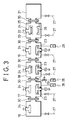
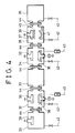
- Figs. 3 and 4 are constitutional views illustrating exemplary apparatuses for manufacturing the solar cells of the present invention.
- the constitution of an amorphous silicon solar cell which can be manufactured by the present invention will be described with reference to Fig. 2.
- the solar cell which can be manufactured by the present invention comprises a substrate 1 and a first electrode 2, a first conductive film 3, a thinner first substantially intrinsic film 4, a thicker second substantially intrinsic film 5, a second conductive film 7 and a second electrode 8 which are stacked on the substrate 1.
- a thinner third substantially intrinsic film 6 may be interposed between the thicker second substantially intrinsic film 5 and the second conductive film 7.
- the thickness of the thicker second substantially intrinsic film must be naturally larger than that of the film formed by one repetition of a film deposition and a modification as described hereinafter, and each of the other films has the same thickness as in a usual amorphous solar cell.
- the thickness of the first electrode 2 is from 1000 ⁇ (100nm) to 5 ⁇ m
- that of the first conductive film 3 is from 10 to 500 ⁇ (1-50nm)
- that of the thinner first substantially intrinsic film 4 is from 10 to 500 ⁇ (1-50nm)
- that of the thicker second substantially intrinsic film 5 is from 500 ⁇ (50nm) to 2 ⁇ m
- that of the thinner third substantially intrinsic film 6 is from 10 to 500 ⁇ (1-50nm)
- that of the second conductive film 7 is from 10 to 500 ⁇ (1-50nm)
- that of the second electrode 8 is from 1000 ⁇ (100nm) to 5 ⁇ m.
- the material of the substrate may have insulating properties or conductive properties, transparency or opaqueness.
- the material of the substrate there can be effectively used a film or a plate of glass, alumina, silicon, stainless steel, aluminum, molybdenum, chromium or a heat-resistant polymer.
- the material of the electrodes is not substantially restricted except that the electrode on a light-incident side must be transparent or have transparency.
- a metal such as aluminum, silver, chromium, titanium, nickel-chromium, gold or platinum, or a metal oxide of tin oxide, zinc oxide or indium oxide.
- the term 'amorphous silicon solar cell' includes amorphous silicon cell, amorphous silicon-germanium alloy cell, amorphous silicon-carbon cell and amorphous silicon-tin alloy cell.
- the electrodes, conductive films and substantially intrinsic films are formed on the substrate, but the formation process of the intrinsic film and conductive film which is the feature of the present invention will be described in detail.
- the present invention is characterized by forming the second substantially intrinsic film by repeating a film deposition step and a modification step.
- the other films, i.e., the first conductive film, the thinner first substantially intrinsic film, the thinner third substantially intrinsic film and the second conductive film can be also formed by repeating the above-mentioned film deposition step and the modification step without impairing the effect of the present invention, and this procedure is rather preferable.
- Typical techniques of the film formation include physical film deposition methods such as vacuum evaporation, sputtering and ion plating as well as chemical vapor deposition (CVD) methods such as photo CVD and plasma CVD.
- CVD chemical vapor deposition
- the modification step is a step achieved by subjecting the film to dehydrohalogenation, and this modification step will be described hereinafter.
- the film deposition step and the modification step are repeated.
- the semiconductor film which is deposited preferably contains 20 atom% or less of bound hydrogen and/or bound deuterium.
- 20 atom% or less of bound hydrogen and/or bound deuterium means that if only bound hydrogen is present, the amount of bound hydrogen is 20 atom% or less, that if only bound deuterium is present, the amount of bound deuterium is 20 atom% or less, or that if bound hydrogen and bound deuterium are both present, the total amount of bound hydrogen and bound deuterium is 20 atom% or less.
- an optical band gap can be changed by regulating the thickness of the semiconductor film which can be deposited in one repetition. That is, it is a preferable embodiment to continuously change the optical band gap by regulating the thickness of the second substantially intrinsic film in a certain repetition.
- the deposited silicon semiconductor film is modified by subjecting the same to dehydrohalogenation.
- this dehydrohalogenation is carried out by bringing the halogenated silicon semiconductor film into contact with a silicon hydride gas or a silicon deuteride gas.
- the dehydrohalogenation is carried out by bringing the hydrogenated silicon semiconductor film or the deuterated silicon semiconductor film into contact with a silicon halide gas. In either case, the dehydrohalogenation is carried out in an atmosphere of a silicon hydride gas, a silicon deuteride gas or a silicon halide gas. In this case, the dehydrohalogenation may be done, while the film is irradiated with light.
- the halogenated silicon semiconductor film is formed by a physical film deposition technique such as vacuum evaporation, sputtering or ion plating, or a chemical vapor deposition (CVD) technique such as photo CVD or plasma CVD.
- a physical film deposition technique such as vacuum evaporation, sputtering or ion plating
- a chemical vapor deposition (CVD) technique such as photo CVD or plasma CVD.
- the dehydrohalogenation step is achieved by introducing silicon hydride or silicon deuteride, while the surface of the film is covered with a halogen atom, and then applying light, heat, ions or the like to the film to bring about a dehydrohalogenation reaction and to thereby bind the silicon atoms of silicon hydride to the film.
- the halogenated semiconductor film of the present invention may contain hydrogen.
- This method is characterized by repeating the film deposition step and the dehydrohalogenation step, and the thickness of the semiconductor film deposited every one repetition is regulated to a level of from 1 ⁇ to 100 ⁇ (0.1-10nm). Film deposition conditions other than this requirement do not have any influence on the effect of the present invention.
- Examples of the starting material for film deposition which can be effectively used in the physical film deposition method include elements, compounds and alloys thereof such as silicon, silicon carbide, silicon nitride, silicon-germanium alloy (or composite powder) and silicon-tin alloy (or composite powder).
- a reactive film deposition method which can be carried out in the atmosphere of fluorine, chlorine or the like is convenient.
- the film containing no halogen can be subjected to a halogen element treatment to obtain a halogenated silicon.
- the substrate temperature of 500°C or less can be employed under conditions that the surface of the deposited film can be covered with the halogen atoms.
- the film deposition may be carried out in an atmosphere of an inert gas, a hydrocarbon, an oxygen gas or the like.
- gas flow rate is from 1 to 100 sccm
- reaction pressure is in the range of from 0.001 mtorr to 10 torr (13 x 10 -5 -1300Nm -2 ).
- the film deposition conditions of the flow rate, the pressure, electric power and the like can be suitably selected in accordance with the deposition rate.
- the substrate temperature is preferably set in accordance with the dehydrohalogenation step, but no restriction is basically put on this temperature. Typically, a temperature of 500°C or less is selected.
- the raw material gas examples include a mixed gas of a silane compound such as a monosilane, a disilane, a trisilane or a tetrasilane represented by the formula Si n H 2n+2 , Si n D 2n+2 or Si n D (2n+2)-m H m (each of n and m is an integer) and a halogen gas such as a chlorine gas or a fluorine gas; a halogenated silane such as monofluorosilane, difluorosilane, trifluorosilane, tetrafluorosilane, monochlorosilane, dichlorosilane or trichlorosilane; a mixed gas of this halogenated silane and hydrogen or deuterium; and a mixed gas of the above-mentioned gas and an organic silane, a hydrocarbon or the like.
- a silane compound such as a monosilane, a disilane, a tris
- hydrogen, deuterium, helium, argon, neon, nitrogen or the like may be introduced together with the raw material gas.
- this kind of gas its effective amount is in the range of from 0.01 to 100% (volume ratio) based on the raw material gas, and it is suitably selected, considering the deposition rate and film characteristics (the amount of hydrogen and the like).
- an ultraviolet light source having a wave length of 350 nm or less such as a low-pressure mercury lamp, a deuterium lamp or a rare gas lamp is used to decompose the raw material gas, so that the film is deposited.
- gas flow rate is preferably from 1 to 100 sccm
- reaction pressure is preferably from 15 mtorr (2Nm -2 ) to atmospheric pressure.
- Substrate temperature is preferably from room temperature to 600°C, and more preferably, it is suitably selected in the range of from 300 to 500°C, considering the film formation time which can be presumed from the heat resistance of the substrate and the deposition rate, the temperature in the dehydrohalogenation step and the like.
- the flow rate of the raw material gas is from 1 to 900 sccm
- reaction pressure is from 1.3 ⁇ 10 -4 Pa (0.001 mtorr) to atmospheric pressure
- electric power is from 1 mW/cm 2 to 10 W/cm 2 .
- Substrate temperature is preferably from room temperature to 600°C, more preferably from 300 to 500°C.
- the dehydrohalogenation step of the deposited semiconductor film can be effected by introducing a silane compound into a dehydrohalogenation chamber, and then applying heat, light, ions or the like to the film.
- the substrate temperature is from 400 to 600°C, preferably from 400 to 500°C.
- the substrate temperature is from room temperature to 600°C, preferably from 200 to 450°C, which is lower temperatures than in the case of heat alone.
- Examples of the effectively usable silane compound include silicon hydride and silicon deuteride such as monosilane, disilane and trisilane.
- dehydrohalogenation reaction is carried out by light irradiation.
- the dehydrohalogenation reaction is carried out by irradiating the surface of the halogenated silicon film with light in the atmosphere of a silicon hydride gas.
- Substrate temperature is from room temperature to 600°C, preferably from 200 to 450°C.
- Reaction pressure is in the range of from 0.13 Pa to 1.34 Pa (1 mtorr to 1 torr), more preferably from 1.3 to 13 Pa (10 mtorr to 100 mtorr).
- light source is suitably selected from a low-pressure mercury lamp, a rare gas discharge lamp, an ultraviolet laser, a deuterium lamp, an Xe pulse lamp, a visual laser, a carbon dioxide gas laser or the like.
- the dehydrohalogenation reaction in the present invention is particularly effective under a low pressure, and rays other than ultraviolet rays can also be effectively utilized. Therefore, it should be noted that the present invention is different from the photo CVD of a conventional technique in technical category. Furthermore, irradiation time can be suitably selected in compliance with the deposition rate of the film.
- a film having a thickness of from 0.1 to 10nm is formed by one operation of the film deposition step.
- the film thickness in the film deposition step can be controlled by regulating a film formation time.
- the deposition rate is from about 0.1 to about 30 ⁇ /second ( ⁇ 01-3nm/s), and therefore, for example, the film formation time is from about 3 seconds to about 1000 seconds.
- the film thickness is in excess of 100 ⁇ (10nm)
- the effect of the subsequent dehydrohalogenation step is spoiled.
- the effect of the present invention is not impaired but this operation is required to be repeated several thousand times to obtain a predetermined total film thickness.
- a time necessary for one cycle is not a requirement which should be particularly restricted, but it is preferably 1000 seconds or less. It is preferred that the transfer time of from the film deposition step to the dehydrohalogenation step and the transfer time of from the dehydrohalogenation step to the film deposition step are as short as possible.
- each transfer time can be regulated to 30 seconds or less.
- the silicon films are formed every one to several atomic layers by repeating the step of the covering of the surface of the deposited film with a halogen and the step of the dehydrohalogenation with silicon hydride or silicon deuteride.
- the thus obtained silicon film contains less microvoids and has high density.
- a hydrogenated silicon or a deuterated silicon semiconductor film can be formed typically by a physical film deposition method such as vacuum evaporation, sputtering or ion plating, or a chemical vapor deposition (CVD) method such as photo CVD or plasma CVD.
- CVD chemical vapor deposition
- the dehydrohalogenation step is achieved by introducing a silicon halide, while the surface of the film is covered with hydrogen or deuterium and simultaneously applying light, heat, ions or the like to the film to advance a dehydrohalogenation reaction and to thereby bind the silicon atoms of silicon halide to the film.
- the present invention is characterized by repeating the film deposition step and the dehydrohalogenation step, and the thickness of the semiconductor film formed every one repetition is preferably regulated to 1-100 ⁇ ( ⁇ 1-10nm). Film deposition conditions other than this requirement do not have any influence on the effect of the present invention.
- Examples of the starting material for the physical film deposition include elements, compounds and alloys such as silicon, silicon carbide, silicon nitride, silicon-germanium alloy (or composite powder) and silicon-tin alloy (or composite powder) can be used.
- a reactive film deposition method in the atmosphere of hydrogen or deuterium is convenient, and after the film formation, the film can be subjected to a hydrogen treatment or a deuterium treatment to obtain a hydrogenated or a deuterated semiconductor film.
- a film deposition temperature of 500°C or less can be employed under conditions that the surface of the deposited film can be covered with hydrogen or deuterium.
- the film deposition may be carried out in an atmosphere of an inert gas, hydrogen, deuterium, a hydrocarbon, fluorine, an oxygen gas or the like without disturbing the object of the present invention.
- gas flow rate is from 1 to 100 sccm
- reaction pressure is in the range of from 0.13 Pa to 134 Pa (0.001 mtorr to 10 torr).
- the film deposition conditions of the gas flow rate, the pressure, electric power and the like can be suitably selected in accordance with the deposition rate.
- the substrate temperature is preferably set in accordance with the dehydrohalogenation step, but no restriction is basically put on this temperature. Typically, a temperature of 500°C or less is selected.
- the raw material gas for the film formation there can be used a silane compound such as monosilane, disilane, trisilane or tetrasilane represented by the formula Si n H 2n+2 , Si n D 2n+2 or Si n D (2n+2)-m H m (each of n and m is an integer), silane fluoride, an organic silane, a hydrocarbon, germanium hydride or germanium fluoride singly or in the form of a mixture thereof.
- hydrogen, deuterium, fluorine, chlorine, helium, argon, neon, nitrogen or the like may be introduced together with the raw material gas.
- this kind of gas is used, its effective amount is in the range of from 0.01 to 100% (volume ratio) of the raw material gas, and it is suitably selected, considering the deposition rate and film characteristics (the amount of hydrogen and the like).
- an ultraviolet light source having a wave length of 350 nm or less such as a low-pressure mercury lamp, a deuterium lamp or a rare gas lamp is used to decompose the raw material gas, whereby the film is deposited.
- gas flow rate is from 1 to 100 sccm
- reaction pressure is from 15 mtorr (2Nm -2 ) to atmospheric pressure
- substrate temperature is from room temperature to 600°C. More preferably, the substrate temperature is suitably selected in the range of from 300 to 500°C, considering the film formation time which can be presumed from the heat resistance of the substrate and the deposition rate, the temperature in the dehydrohalogenation step and the like.
- the plasma CVD as a discharge system, there can be effectively used a radio-frequency discharge system, a direct current discharge system, a microwave discharge system or an ECR discharge system.
- the flow rate of the raw material gas is from 1 to 900 sccm
- reaction pressure is from 1.3 ⁇ 10 -4 Pa (0.001 mtorr) to atmospheric pressure
- electric power is from 1 mW/cm 2 to 10 W/cm 2 .
- These film deposition conditions can be suitably changed in accordance with the deposition rate and the discharge system.
- the substrate temperature is preferably from room temperature to 600°C, more preferably from 300 to 500°C.
- the dehydrohalogenation step of the deposited semiconductor film can be effected by introducing a silicon halide into a dehydrohalogenation chamber, and then applying heat, light, ions or the like to the film.
- the substrate temperature is from 400 to 600°C, preferably from 400 to 500°C.
- the substrate temperature is from room temperature to 600, preferably from 200 to 450°C, which is lower temperatures than in the case of heat. It is a preferable means to use heat, light and ions together.
- the reaction pressure is in the range of from 0.13Pa to 1.34Pa (1 mtorr to 1 torr), more preferably from 1.3 to 13Pa (10 mtorr to 100 mtorr).
- the reaction conditions are the substantially same as in the case of using the above-mentioned silicon hydride gas.
- the silicon halide which can be used in the dehydrohalogenation step is a compound obtained by replacing hydrogen of silicon hydride (hereinafter referred to simply as "silane") with a halogen atom
- examples of the silicon halide include silane halides, disilane halides and trisilane halides.
- the effective halogen atom include fluorine, chlorine and bromine.
- Typical examples of the silicon halide include monofluorosilane, difluorosilane, trifluorosilane, monochlorosilane, dichlorosilane, trichlorosilane, monofluorodisilane, difluorodisilane, monochlorodisilane and dichlorodisilane.
- One operation of the film deposition step provide the film having a thickness of from 1 to 100 ⁇ ( ⁇ 1-10nm).
- the deposition of the film having a thickness of 100 ⁇ (10nm) or less can be controlled by regulating the film formation time.
- the film formation time is, for example, from about 3 seconds to 1000 seconds.
- the film having an extremely small thickness e.g., a thickness of less than 1 ⁇ ( ⁇ 1nm) is formed by one operation of the film deposition
- this operation is required to be repeated several thousand times to obtain a predetermined total film thickness, though the effect of the present invention is not impaired.
- a time necessary for one cycle is not a requirement which should be particularly restricted, but it is preferably 1000 seconds or less. It is preferred that the transfer time of from the film deposition step to the dehydrohalogenation step and the transfer time of from the dehydrohalogenation step to the film deposition step are as short as possible. These transfer times depend upon the shape and size of an apparatus, a vacuum evacuation system and the like. In the concrete, each transfer time can be shortened to 30 seconds or less.
- the film deposition step and the dehydrohalogenation step may be performed in the same reaction chamber or separated chambers without impairing the effect of the present invention. No particular restriction is put on the thickness of the film formed by repeating the film deposition step and the dehydrohalogenation step, but it is usually from about 10 ⁇ (1nm) to about 10 ⁇ m.
- the silicon films are formed every one to several atomic layers by repeating the step of the covering of the surface of deposited film with hydrogen and the step of the dehydrohalogenation with a silicon halide.
- the thus obtained silicon film contains much less microvoids and has high density.
- Figs. 1 and 2 show the schematic diagram of layered structure of amorphous silicon solar cells obtained by the present invention.
- reference numeral 1 is a substrate
- numeral 2 is a first electrode
- 3 is a first conductive film
- 4 is a thinner first substantially intrinsic film
- 5 is a thicker second substantially intrinsic film
- 6 is a thinner third substantially intrinsic film
- 7 is a second conductive film
- 8 is the second electrode.
- reference numeral 1 is the substrate
- numeral 2 is the first electrode
- 3 is the first conductive film
- 4 is the thinner first substantially intrinsic film
- 5 is the thicker second substantially intrinsic film
- 7 is the second conductive film
- 8 is the second electrode.
- Fig. 3 is a schematic view illustrating one embodiment of a preferable apparatus for preparing a solar cell of the present invention.
- reference numeral 16 is a substrate loading chamber
- numeral 17 is a first conductive film formation chamber
- 18 is a thicker second substantially intrinsic film formation chamber
- 19 is a second conductive film formation chamber
- 20 is a second electrode formation chamber
- 21 is a substrate unloading chamber
- 22 is a substrate
- 23 is a radio-frequency electrode
- 24 is a substrate heating electrode
- 25 is a metal mask
- 26 is an evaporation source
- 27 is a vacuum evacuation line
- 28 is a raw material gas introduction line
- 29 is a three-way valve
- 30 is a gate valve.
- Fig. 4 shows a schematic view illustrating another embodiment of a preferable apparatus for preparing the solar cell of the present invention.
- reference numeral 31 is a substrate loading chamber
- numeral 32 is a first conductive film formation chamber
- 33 is a thicker second substantially intrinsic film formation chamber
- 34 is a second conductive film formation chamber
- 35 is a second electrode formation chamber
- 36 is a substrate unloading chamber
- 37 is a substrate
- 38 is a-radio-frequency electrode
- 39 is a substrate heating electrode
- 40 is a metal mask
- 41 is an evaporation source
- 42 is a vacuum evacuation line
- 43 is a raw material gas introduction line
- 44 is a gate valve.
- the sectional schematic views illustrating examples of layered structure of the amorphous silicon solar cells manufactured by the above-mentioned method are shown in Figs. 1 and 2.
- the first and second conductive types are different from each other, and if one is p-type, the other is n-type.
- the materials of the first and second electrodes depend upon the transparency of the substrate and a light-incident direction. For example, if the transparent glass substrate is used and light is incident from this glass side, tin oxide or the like which is a transparent conductive film must be applied to the first electrode.
- the first electrode may be made of a metal such as silver or aluminum, but the second electrode must be the transparent conductive film.
- Figs. 3 and 4 show schematic views illustrating preferable apparatus for forming the elements of the present invention.
- the respective chambers are comparted with the gate valves, and the substrate can be delivered to the respective chambers without breaking a vacuum state by mechanisms for opening and closing these valves and substrate delivery mechanisms.
- Each of the first and second conductive film formation chambers 17, 19 has a function capable of applying a usual plasma CVD method. The employment of the conductive film formation chambers 17, 19 permits forming the thinner first substantially intrinsic film and the thinner third substantially intrinsic film.
- the second electrode formation chamber 20 has the function of vacuum evaporation or sputtering by which the electrode can be formed.
- the thicker second substantially intrinsic film formation chamber which is the feature of the present invention has the function of the usual plasma CVD method and a gas feed switch device capable of switching the feed of raw material gases.
- the thicker second substantially intrinsic film formation chamber is further divided into the two chambers of an exclusive film deposition chamber and an exclusive modification chamber. The combination of these two chambers can be selected from the group consisting of vacuum evaporation, sputtering, ion plating, photo CVD, plasma CVD and the like. This constitution is disclosed in detail in EP-A-407088, and an optional combination of these devices can be possible.
- a film formation apparatus for the practice of the present invention, there was used such an apparatus as shown in Fig. 3.
- This apparatus comprises a substrate loading chamber, a first conductive film formation chamber, a thicker second substantially intrinsic film formation chamber, a second conductive film formation chamber and a second electrode formation chamber, and in all the members except the substrate loading chamber and the electrode formation chamber, a plasma CVD method could be applied.
- the layered structure of an amorphous silicon solar cell which could be obtained herein is shown in Fig. 2.
- As the first electrode 2 a glass substrate 1 on which a tin oxide film was formed was heated in vacuum in the substrate loading chamber and then transferred to the first conductive film formation chamber.
- a thinner first substantially intrinsic film 4 having a thickness of about 150 ⁇ (15nm) was formed under a pressure of 13 Pa (0.1 Torr) at a substrate temperature of 275°C at a radio-frequency electric power of 1 W.
- the substrate was delivered to the thicker second substantially intrinsic film formation chamber.
- This thicker second substantially intrinsic film formation chamber was composed of the two chambers of a film deposition chamber and a dehydrohalogenation chamber. The temperature of the substrate was set to 300°C, and 10 sccm of a mixed gas of trichlorosilane and hydrogen was introduced as a raw material.
- An Si film having about 40 ⁇ (4nm) was deposited under a pressure of 0.008 torr (1 Nm -2 ) in the film deposition chamber by the application of a radio-frequency electric power of 10 W and then transferred to the dehydrohalogenation chamber.
- Disilane was introduced into the dehydrohalogenation chamber, and a chlorinated and hydrogenated silicon film was exposed to ultraviolet rays from an ultraviolet lamp under a pressure of 13 Pa (0.1 torr) for 30 seconds.
- the substrate having the film thereon was returned to the film deposition chamber, and the cycle operation of the film deposition step and the dehydrohalogenation step was repeated 150 times to obtain a thickness of about 6000 ⁇ (600nm).
- the substrate having the thus formed film was transferred to a second conductive film formation chamber.
- the film was transferred to the second electrode formation chamber, and an aluminium film was formed thereon as a second electrode 8 by vacuum evaporation.
- the photovoltaic conversion properties of the thus obtained amorphous silicon solar cell were measured under the irradiation of AM-1.5 and 100 mW/cm 2 by means of a solar simulator. As a result, a photovoltaic conversion efficiency was 12.7%, a short-circuit current was 18.49 mA/cm 2 , an open circuit voltage was 0.895V, and a fill factor was 0.767, which meant that the solar cell had excellent performance.
- this cell was continuously irradiated with light of AM-1.5 and 100 mW/cm 2 for 20 hours to observe the change of the photovoltaic conversion efficiency.
- the change of the photovoltaic conversion efficiency after 20 hours with respect to an initial photovoltaic conversation efficiency was 1% or less, which meant that the above-mentioned amorphous silicon solar cell was extremely excellent in stability.
- Example 1 after the formation of a halogenated Si film, film formation was made to obtain a thickness of 6000 ⁇ (600nm) without passing through a dehydrohalogenation step, thereby preparing an amorphous silicon solar cell.
- a photovoltaic conversion efficiency was 11.0%
- a short-circuit current was 17.85 mA/cm 2
- an open circuit voltage was 0.890 V
- a fill factor was 0.692, which meant that the solar cell in this comparative example was poorer in performance than the cell in Example 1.
- the light-stability of the cell was measured, and as a result, the change rate of the photovoltaic conversion efficiency after light irradiation for 20 hours was about 23%, which meant that the light-stability was insufficient.
- a film was formed by repeating film deposition and modification by dehydrohalogenation. That is, a substrate on which the film formation was made until a thinner first substantially intrinsic film in the same manner as in Example 1 was transferred to a thicker second substantially intrinsic film formation chamber.
- This thicker second substantially intrinsic film formation chamber was composed of the two chambers of a film deposition chamber and a dehydrohalogenation chamber. The temperature of the substrate was set to 300°C, and as starting materials, a high-purity silicon target was set to a cathode, and 10 sccm of a mixed gas of argon and hydrogen was introduced into the film deposition chamber.
- An Si film having a thickness of about 40 ⁇ (4nm) was deposited by applying a radio-frequency electric power of 100 W under a pressure of 0.08 Pa (0.6 mtorr) in the film deposition chamber in accordance with a radio-frequency magnetron sputtering method, and the thus deposited film was then transferred to the dehydrohalogenation chamber.
- Monochlorosilane was introduced into the dehydrohalogenation chamber, and the hydrogenated silicon film was exposed to ultraviolet rays from an ultraviolet lamp under a pressure of 13 Pa (0.1 torr) for 30 seconds.
- the substrate having the film thereon was returned to the film deposition chamber, and the cycle operation of the film deposition step and the dehydrohalogenation step was repeated 150 times under the same conditions to obtain a thickness of about 6000 ⁇ (600nm). Afterward, the substrate having the film was transferred to a second conductive film formation chamber, and afterward the same operation as in Example 1 was carried out again.
- the photovoltaic conversion properties of the thus obtained amorphous silicon solar cell were measured under the irradiation of AM-1.5 and 100 mW/cm 2 by means of a solar simulator. As a result, a photovoltaic conversion efficiency was 12.6%, a short-circuit current was 18.29 mA/cm 2 , an open circuit voltage was 0.897 V, and a fill factor was 0.768, which meant that the solar cell had excellent performance.
- this cell was continuously irradiated with light of AM-1.5 and 100 mW/cm 2 for 20 hours to observe the change of the photovoltaic conversion efficiency. The change of the photovoltaic conversion efficiency after 20 hours with respect to an initial photovoltaic conversion efficiency was 2% or less, which meant that the above-mentioned amorphous silicon solar cell was extremely excellent in stability.
- a hydrogenated silicon film having a thickness of 6000 ⁇ (600nm) was formed without passing through a dehydrohalogenation step after the film deposition, thereby preparing an amorphous silicon solar cell.
- a photovoltaic conversion efficiency was 10.7%
- a short-circuit current was 17.55 mA/cm 2
- an open circuit voltage was 0.885 V
- a fill factor was 0.689, which meant that the solar cell in this comparative example was poorer in performance than the cell in Example 2.
- the light-stability of the cell was measured, and as a result, the change rate of the photovoltaic conversion efficiency after light irradiation for 20 hours was about 27%, which meant that the stability was insufficient.
- a thicker second substantially intrinsic film is prepared by depositing a film having a thickness of at least 1 to 100 ⁇ ( ⁇ 1-10nm) by one repetition, and the thus deposited film is treated with a non-deposition and reactive gas in a modification step to prepare an amorphous silicon solar cell, and this cell has better photovoltaic characteristics as compared with an amorphous silicon solar cell prepared without subjecting the film to the modification step. Accordingly, in the solar cell of the present invention, stability to light irradiation and other characteristics which involve conventional substantial problems can be remarkably improved. In consequence, the present invention can provide a technique which permits high conversion efficiency and high reliability required in solar cells for electric power, and thus it is an extremely useful invention in an energy industry.
Landscapes
- Photovoltaic Devices (AREA)
Claims (6)
- Verfahren zur Herstellung einer Solarzelle aus amorphem Silicium, welches die Herstellung einer ersten Elektrode, eines ersten leitenden Films, eines dünneren ersten, im wesentlichen intrinsischen Films, eines dickeren zweiten, im wesentlichen intrinsischen Films, eines zweiten leitenden Films, dessen Leitfähigkeit sich von der des ersten leitenden Films unterscheidet, und eine zweite Elektrode in dieser Reihenfolge auf einem Träger umfaßt;
wobei dieses Verfahren dadurch gekennzeichnet ist, daß mindestens der dickere zweite, im wesentlichen intrinsische Film durch die aufeinanderfolgenden Schritte gebildet wird:(a) Abscheidung eines Silicium-Halbleiterfilms bis zu einer Dicke von 0,1 bis 10 nm, wobei die Schicht ein halogenierter Film ist, der als solcher abgeschieden wird, oder ein halogenierter Film, der ohne Halogen abgeschieden wurde und dann einer Behandlung mit einem Halogenelement unterzogen wurde; und dann(b) Modifizierung des abgeschiedenen Films, indem dieser einer Dehydrohalogenierung unterzogen wird, und die Abfolge der Schritte (a) und (b) mehrmals wiederholt wird. - Verfahren zur Herstellung einer Solarzelle aus amorphem Silicium nach Anspruch 1, worin ein dünnerer dritter, im wesentlichen intrinsischer Film zwischen dem dickeren zweiten, im wesentlichen intrinsischen Film und dem zweiten leitenden Film gebildet wird.
- Verfahren zur Herstellung einer Solarzelle aus amorphem Silicium nach Anspruch 1, worin weiterhin der Silicium-Halbleiterfilm ein halogenierter Silicium-Halbleiterfilm ist, und der Dehydrohalogenierungsschritt durchgeführt wird, indem der halogenierte Silicium-Halbleiterfilm mit einem Siliciumhydridgas in Kontakt gebracht wird.
- Verfahren zur Herstellung einer Solarzelle aus amorphem Silicium nach Anspruch 3, worin die Dehydrohalogenierung mittels Lichtbestrahlung durchgeführt wird.
- Verfahren zur Herstellung einer Solarzelle aus amorphem Silicium nach Anspruch 1, worin der Silicium-Halbleiterfilm ein hydrierter Silicium-Halbleiterfilm ist, und der Dehydrohalogenierungsschritt durchgeführt wird, indem der hydrierte Silicium-Halbleiterfilm mit einem Siliciumhalogenidgas in Kontakt gebracht wird.
- Verfahren zur Herstellung einer Solarzelle aus amorphem Silicium nach Anspruch 5, worin die Dehydrohalogenierung mittels Lichtbestrahlung durchgeführt wird.
Applications Claiming Priority (6)
| Application Number | Priority Date | Filing Date | Title |
|---|---|---|---|
| JP234393/90 | 1990-09-06 | ||
| JP234392/90 | 1990-09-06 | ||
| JP234391/90 | 1990-09-06 | ||
| JP2234393A JP2966909B2 (ja) | 1990-09-06 | 1990-09-06 | 非晶質半導体薄膜 |
| JP2234392A JPH04115579A (ja) | 1990-09-06 | 1990-09-06 | 非晶質太陽電池 |
| JP2234391A JP2966908B2 (ja) | 1990-09-06 | 1990-09-06 | 光電変換素子 |
Publications (3)
| Publication Number | Publication Date |
|---|---|
| EP0475666A2 EP0475666A2 (de) | 1992-03-18 |
| EP0475666A3 EP0475666A3 (en) | 1992-08-05 |
| EP0475666B1 true EP0475666B1 (de) | 1997-04-09 |
Family
ID=27332132
Family Applications (1)
| Application Number | Title | Priority Date | Filing Date |
|---|---|---|---|
| EP91308087A Expired - Lifetime EP0475666B1 (de) | 1990-09-06 | 1991-09-04 | Verfahren zur Herstellung einer Solarzelle aus amorphem Silizium |
Country Status (4)
| Country | Link |
|---|---|
| US (1) | US5248348A (de) |
| EP (1) | EP0475666B1 (de) |
| AU (1) | AU632241B2 (de) |
| DE (1) | DE69125554T2 (de) |
Families Citing this family (29)
| Publication number | Priority date | Publication date | Assignee | Title |
|---|---|---|---|---|
| US5419783A (en) * | 1992-03-26 | 1995-05-30 | Sanyo Electric Co., Ltd. | Photovoltaic device and manufacturing method therefor |
| WO1994000869A1 (en) * | 1992-06-29 | 1994-01-06 | United Solar Systems Corporation | Microwave energized deposition process with substrate temperature control |
| US5476798A (en) * | 1992-06-29 | 1995-12-19 | United Solar Systems Corporation | Plasma deposition process with substrate temperature control |
| DE69410301T2 (de) * | 1993-01-29 | 1998-09-24 | Canon Kk | Verfahren zur Herstellung funktioneller niedergeschlagener Schichten |
| JPH06326024A (ja) * | 1993-05-10 | 1994-11-25 | Canon Inc | 半導体基板の製造方法及び非晶質堆積膜の形成方法 |
| WO1995026571A1 (en) * | 1994-03-25 | 1995-10-05 | Amoco/Enron Solar | Stabilized amorphous silicon and devices containing same |
| US5635408A (en) * | 1994-04-28 | 1997-06-03 | Canon Kabushiki Kaisha | Method of producing a semiconductor device |
| US5518935A (en) * | 1994-06-17 | 1996-05-21 | At&T Corp. | Hydrogenation of photoresponsive semiconductor devices |
| US6489219B1 (en) | 1995-11-09 | 2002-12-03 | Micron Technology, Inc. | Method of alloying a semiconductor device |
| US20020031920A1 (en) | 1996-01-16 | 2002-03-14 | Lyding Joseph W. | Deuterium treatment of semiconductor devices |
| US5872387A (en) * | 1996-01-16 | 1999-02-16 | The Board Of Trustees Of The University Of Illinois | Deuterium-treated semiconductor devices |
| US6077791A (en) * | 1996-12-16 | 2000-06-20 | Motorola Inc. | Method of forming passivation layers using deuterium containing reaction gases |
| US6252270B1 (en) * | 1997-04-28 | 2001-06-26 | Agere Systems Guardian Corp. | Increased cycle specification for floating-gate and method of manufacture thereof |
| US6023093A (en) * | 1997-04-28 | 2000-02-08 | Lucent Technologies Inc. | Deuterated direlectric and polysilicon film-based semiconductor devices and method of manufacture thereof |
| US6071751A (en) * | 1997-04-28 | 2000-06-06 | Texas Instruments Incorporated | Deuterium sintering with rapid quenching |
| US5982020A (en) | 1997-04-28 | 1999-11-09 | Lucent Technologies Inc. | Deuterated bipolar transistor and method of manufacture thereof |
| US6365511B1 (en) | 1999-06-03 | 2002-04-02 | Agere Systems Guardian Corp. | Tungsten silicide nitride as a barrier for high temperature anneals to improve hot carrier reliability |
| US6468829B2 (en) | 2000-05-16 | 2002-10-22 | United Solar Systems Corporation | Method for manufacturing high efficiency photovoltaic devices at enhanced depositions rates |
| US6576522B2 (en) | 2000-12-08 | 2003-06-10 | Agere Systems Inc. | Methods for deuterium sintering |
| US6605529B2 (en) | 2001-05-11 | 2003-08-12 | Agere Systems Inc. | Method of creating hydrogen isotope reservoirs in a semiconductor device |
| JP4733519B2 (ja) * | 2002-10-25 | 2011-07-27 | エリコン ソーラー アーゲー,トゥルーバッハ | 半導体装置の製造方法及びこの方法で得られた半導体装置 |
| US7790574B2 (en) | 2004-12-20 | 2010-09-07 | Georgia Tech Research Corporation | Boron diffusion in silicon devices |
| US8309387B2 (en) * | 2007-04-13 | 2012-11-13 | David Forehand | Improving back-contact performance of group VI containing solar cells by utilizing a nanoscale interfacial layer |
| US20110226330A1 (en) * | 2008-08-23 | 2011-09-22 | The Regents Of The University Of California | Amorphous silicon solar cells |
| EP2437306A4 (de) * | 2009-05-28 | 2013-10-02 | Toyo Kohan Co Ltd | Substrat für eine verbundhalbleitersolarzelle |
| US8778448B2 (en) | 2011-07-21 | 2014-07-15 | International Business Machines Corporation | Method of stabilizing hydrogenated amorphous silicon and amorphous hydrogenated silicon alloys |
| US9157146B2 (en) * | 2011-08-02 | 2015-10-13 | Shincron Co., Ltd. | Method for depositing silicon carbide film |
| JP6306411B2 (ja) * | 2014-04-17 | 2018-04-04 | 株式会社日立国際電気 | 半導体装置の製造方法、基板処理装置およびプログラム |
| CN115985803B (zh) * | 2023-03-22 | 2023-07-04 | 广东联塑班皓新能源科技集团有限公司 | 一种光伏组件生产系统 |
Family Cites Families (8)
| Publication number | Priority date | Publication date | Assignee | Title |
|---|---|---|---|---|
| US4379943A (en) * | 1981-12-14 | 1983-04-12 | Energy Conversion Devices, Inc. | Current enhanced photovoltaic device |
| JPS59107574A (ja) * | 1982-12-13 | 1984-06-21 | Agency Of Ind Science & Technol | アモルフアスシリコン太陽電池の製造方法 |
| US4471155A (en) * | 1983-04-15 | 1984-09-11 | Energy Conversion Devices, Inc. | Narrow band gap photovoltaic devices with enhanced open circuit voltage |
| JPS62177983A (ja) * | 1986-01-31 | 1987-08-04 | Mitsui Toatsu Chem Inc | 光電変換素子の製造法 |
| US4690830A (en) * | 1986-02-18 | 1987-09-01 | Solarex Corporation | Activation by dehydrogenation or dehalogenation of deposition feedstock and dopant materials useful in the fabrication of hydrogenated amorphous silicon alloys for photovoltaic devices and other semiconductor devices |
| US4799968A (en) * | 1986-09-26 | 1989-01-24 | Sanyo Electric Co., Ltd. | Photovoltaic device |
| JPH06105691B2 (ja) * | 1988-09-29 | 1994-12-21 | 株式会社富士電機総合研究所 | 炭素添加非晶質シリコン薄膜の製造方法 |
| JP2846651B2 (ja) * | 1989-03-31 | 1999-01-13 | 三洋電機株式会社 | 光起電力装置 |
-
1991
- 1991-09-02 AU AU83546/91A patent/AU632241B2/en not_active Ceased
- 1991-09-04 EP EP91308087A patent/EP0475666B1/de not_active Expired - Lifetime
- 1991-09-04 DE DE69125554T patent/DE69125554T2/de not_active Expired - Fee Related
- 1991-09-05 US US07/756,219 patent/US5248348A/en not_active Expired - Fee Related
Also Published As
| Publication number | Publication date |
|---|---|
| DE69125554T2 (de) | 1997-07-17 |
| EP0475666A2 (de) | 1992-03-18 |
| US5248348A (en) | 1993-09-28 |
| EP0475666A3 (en) | 1992-08-05 |
| AU8354691A (en) | 1992-03-12 |
| DE69125554D1 (de) | 1997-05-15 |
| AU632241B2 (en) | 1992-12-17 |
Similar Documents
| Publication | Publication Date | Title |
|---|---|---|
| US5248348A (en) | Amorphous silicon solar cell and method for manufacturing the same | |
| JP2984537B2 (ja) | 光起電力素子 | |
| US5352300A (en) | Solar cell | |
| JPH07123112B2 (ja) | p形アモルファス半導体を堆積させる方法及び電子写真用光受容体の製造方法 | |
| JPH07123111B2 (ja) | 半導体膜の製造方法及び光起電力構造体の製造方法 | |
| JPH02155225A (ja) | 非晶質半導体薄膜の形成方法 | |
| US20010023971A1 (en) | Film forming method and film forming apparatus as well as silicon-based film, photovoltaic device and solar cell, sensor and image pick-up device using the same | |
| JP2788799B2 (ja) | 太陽電池 | |
| US6803080B2 (en) | Method of forming crystalline silicon film by CVD | |
| JP2785882B2 (ja) | 光起電力素子及びその製造方法 | |
| JP3142682B2 (ja) | 太陽電池製造方法及び製造装置 | |
| JP3746607B2 (ja) | シリコン系薄膜光電変換装置の製造方法 | |
| EP0407088B1 (de) | Verfahren zur Herstellung einer amorphen Halbleiterschicht | |
| JPH06260665A (ja) | 非晶質太陽電池 | |
| JPH05102502A (ja) | 非晶質太陽電池 | |
| JPH04115578A (ja) | 光電変換素子 | |
| JPH07183550A (ja) | 非晶質光電変換素子 | |
| JP2966909B2 (ja) | 非晶質半導体薄膜 | |
| JP2000243987A (ja) | 太陽電池装置およびその製造方法 | |
| JP3483549B2 (ja) | 堆積膜形成方法および堆積膜形成装置 | |
| JPH0364019A (ja) | 半導体薄膜 | |
| JP2000196122A (ja) | 光起電力素子 | |
| JP2000232073A (ja) | 多結晶シリコン膜 | |
| JPH04326577A (ja) | 光電変換素子 | |
| JPH08181079A (ja) | 非晶質半導体薄膜形成方法 |
Legal Events
| Date | Code | Title | Description |
|---|---|---|---|
| PUAI | Public reference made under article 153(3) epc to a published international application that has entered the european phase |
Free format text: ORIGINAL CODE: 0009012 |
|
| 17P | Request for examination filed |
Effective date: 19911025 |
|
| AK | Designated contracting states |
Kind code of ref document: A2 Designated state(s): DE FR GB IT |
|
| PUAL | Search report despatched |
Free format text: ORIGINAL CODE: 0009013 |
|
| AK | Designated contracting states |
Kind code of ref document: A3 Designated state(s): DE FR GB IT |
|
| 17Q | First examination report despatched |
Effective date: 19940722 |
|
| GRAG | Despatch of communication of intention to grant |
Free format text: ORIGINAL CODE: EPIDOS AGRA |
|
| GRAH | Despatch of communication of intention to grant a patent |
Free format text: ORIGINAL CODE: EPIDOS IGRA |
|
| GRAH | Despatch of communication of intention to grant a patent |
Free format text: ORIGINAL CODE: EPIDOS IGRA |
|
| RBV | Designated contracting states (corrected) |
Designated state(s): DE FR |
|
| GRAA | (expected) grant |
Free format text: ORIGINAL CODE: 0009210 |
|
| AK | Designated contracting states |
Kind code of ref document: B1 Designated state(s): DE FR |
|
| REF | Corresponds to: |
Ref document number: 69125554 Country of ref document: DE Date of ref document: 19970515 |
|
| ET | Fr: translation filed | ||
| PLBE | No opposition filed within time limit |
Free format text: ORIGINAL CODE: 0009261 |
|
| STAA | Information on the status of an ep patent application or granted ep patent |
Free format text: STATUS: NO OPPOSITION FILED WITHIN TIME LIMIT |
|
| 26N | No opposition filed | ||
| REG | Reference to a national code |
Ref country code: FR Ref legal event code: TP |
|
| PGFP | Annual fee paid to national office [announced via postgrant information from national office to epo] |
Ref country code: FR Payment date: 19980909 Year of fee payment: 8 |
|
| PGFP | Annual fee paid to national office [announced via postgrant information from national office to epo] |
Ref country code: DE Payment date: 19980914 Year of fee payment: 8 |
|
| PG25 | Lapsed in a contracting state [announced via postgrant information from national office to epo] |
Ref country code: FR Free format text: LAPSE BECAUSE OF NON-PAYMENT OF DUE FEES Effective date: 20000531 |
|
| PG25 | Lapsed in a contracting state [announced via postgrant information from national office to epo] |
Ref country code: DE Free format text: LAPSE BECAUSE OF NON-PAYMENT OF DUE FEES Effective date: 20000701 |
|
| REG | Reference to a national code |
Ref country code: FR Ref legal event code: ST |