EP0483824B1 - Transistor MIS avec hétérojunction - Google Patents
Transistor MIS avec hétérojunction Download PDFInfo
- Publication number
- EP0483824B1 EP0483824B1 EP91118558A EP91118558A EP0483824B1 EP 0483824 B1 EP0483824 B1 EP 0483824B1 EP 91118558 A EP91118558 A EP 91118558A EP 91118558 A EP91118558 A EP 91118558A EP 0483824 B1 EP0483824 B1 EP 0483824B1
- Authority
- EP
- European Patent Office
- Prior art keywords
- source
- semiconductor material
- channel
- mis transistor
- transistor
- Prior art date
- Legal status (The legal status is an assumption and is not a legal conclusion. Google has not performed a legal analysis and makes no representation as to the accuracy of the status listed.)
- Expired - Lifetime
Links
Images















Classifications
-
- H—ELECTRICITY
- H10—SEMICONDUCTOR DEVICES; ELECTRIC SOLID-STATE DEVICES NOT OTHERWISE PROVIDED FOR
- H10D—INORGANIC ELECTRIC SEMICONDUCTOR DEVICES
- H10D30/00—Field-effect transistors [FET]
- H10D30/01—Manufacture or treatment
- H10D30/021—Manufacture or treatment of FETs having insulated gates [IGFET]
- H10D30/031—Manufacture or treatment of FETs having insulated gates [IGFET] of thin-film transistors [TFT]
- H10D30/0321—Manufacture or treatment of FETs having insulated gates [IGFET] of thin-film transistors [TFT] comprising silicon, e.g. amorphous silicon or polysilicon
- H10D30/0323—Manufacture or treatment of FETs having insulated gates [IGFET] of thin-film transistors [TFT] comprising silicon, e.g. amorphous silicon or polysilicon comprising monocrystalline silicon
-
- H—ELECTRICITY
- H10—SEMICONDUCTOR DEVICES; ELECTRIC SOLID-STATE DEVICES NOT OTHERWISE PROVIDED FOR
- H10D—INORGANIC ELECTRIC SEMICONDUCTOR DEVICES
- H10D30/00—Field-effect transistors [FET]
- H10D30/60—Insulated-gate field-effect transistors [IGFET]
- H10D30/67—Thin-film transistors [TFT]
- H10D30/6704—Thin-film transistors [TFT] having supplementary regions or layers in the thin films or in the insulated bulk substrates for controlling properties of the device
- H10D30/6713—Thin-film transistors [TFT] having supplementary regions or layers in the thin films or in the insulated bulk substrates for controlling properties of the device characterised by the properties of the source or drain regions, e.g. compositions or sectional shapes
-
- H—ELECTRICITY
- H10—SEMICONDUCTOR DEVICES; ELECTRIC SOLID-STATE DEVICES NOT OTHERWISE PROVIDED FOR
- H10D—INORGANIC ELECTRIC SEMICONDUCTOR DEVICES
- H10D30/00—Field-effect transistors [FET]
- H10D30/60—Insulated-gate field-effect transistors [IGFET]
- H10D30/67—Thin-film transistors [TFT]
- H10D30/6704—Thin-film transistors [TFT] having supplementary regions or layers in the thin films or in the insulated bulk substrates for controlling properties of the device
- H10D30/6713—Thin-film transistors [TFT] having supplementary regions or layers in the thin films or in the insulated bulk substrates for controlling properties of the device characterised by the properties of the source or drain regions, e.g. compositions or sectional shapes
- H10D30/6715—Thin-film transistors [TFT] having supplementary regions or layers in the thin films or in the insulated bulk substrates for controlling properties of the device characterised by the properties of the source or drain regions, e.g. compositions or sectional shapes characterised by the doping profiles, e.g. having lightly-doped source or drain extensions
Definitions
- a metal electrode of the source portion is provided outside the depletion layer region of the PN junction between the source and channel portions and inside the diffusion length L d from the depletion edge on the source side, and the metal electrode is extended to the ground insulating substrate.
- the present invention provides an MIS transistor which has improved resistance to the kink phenomenon, an increased source-drain endurance voltage, which comprises the source and drain regions with sufficiently low parasitic resistance and which can be operated at high speed.
- the thin film SOI transistor is investigated as a transistor having short channel resistance for inhibiting the short channel effect. Since the thin film SOI transistor has the effect of inhibiting the short channel effect and the effects of improving the mobility at the boundary between the gate and the insulating film by relieving the vertical electrical field, decreasing the junction capacity between the source and drain portions and decreasing dark current, the SOI transistor permits further increases in the operating speed and the quality.
- the MIS transistor containing heterojunctions and the source and drain portions made of a semiconductor material having a energy band gap narrower than that of a semiconductor material used for the channel portion does not have the above problem.
- a thin film SOI transistor sometimes produces the problem that thinning of the semiconductor layer and the submicronization of the gate make the parasitic resistance component of the source and drain regions significant, as compared with on resistance, thereby deteriorating the driving force of the transistor.
- the ratio of Ge/Si is at least 1%.
- Such a material is not limited to the Si-Ge type, and, in a GaAsSb type, GaAs 1-x Sb x can be used as the first semiconductor material, and a compound semiconductor such as GaAs 1-y Sb y (wherein x ⁇ y) can be used.
- a compound semiconductor such as GaAs 1-y Sb y (wherein x ⁇ y) can be used.
- Other types of semiconductors such as an InPAs type can also be used.
- the energy band of the second semiconductor material preferably has a conduction band with an energy edge substantially equal to that of the first semiconductor material, and a valence band with an energy edge (electron energy) higher than that of the first semiconductor material. This is because the holes accumulated in the channel portion can be discharged without inhibiting the flow of the electrons in the source region.
- the mixed crystal rate x of the mixed crystal Si x Ge 1-x at least in the source portion is 0.12 or less so that the source and drain regions has a low resistance. The reasons for this are described below.
- the use of the region with a mixed crystal rate x of 0.12 or less thus permits an attempt to be made to decrease the resistance of the source and drain regions.
- this region is useful from the viewpoint of recovery of the damage produced by ion implantation.
- the resistance to the kink phenomenon and the source-drain endurance voltage of the MIS transistor comprising the source portion made of the mixed crystal Si x Ge 1-x with a mixed crystal rate x of 0.12 or less are further improved, for example, in the case of a NMOS thin film SOL transistor, it is necessary to increase only the injection of holes into the source from the channel.
- the kink phenomenon or deterioration in the source-drain endurance voltage is produced due to an increase in the substrate potential, which is caused by the accumulation, in the channel portion, of the holes serving as non-transport carriers among the electron-hole pairs generated at the drain edge by the impact ionization.
- an increase in the substrate potential lowers the potential barrier between the source and channel and thus causes the flow of a large quantity of current into the drain from the source. It is thus effective to cause the holes to efficiently flow in the source electrode, without lowering the potential barrier, i.e., while maintaining the good operation of the MOS transistor.
- the semiconductor energy gap Eg1 of the channel portion is greater than the semiconductor energy gap Eg2 of the source portion.
- the holes generated at the drain edge by impact ionization first flow into the channel portion.
- the potential barrier between the source and channel is low, the holes are easily discharged to the source. Since no hole is thus accumulated in the channel portion without producing the substrate floating effect, good saturation properties and a high drain endurance voltage can be obtained.
- the semiconductor energy gap Eg1 of the channel portion is smaller than the semiconductor energy gap Eg2 of the source portion.
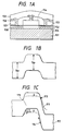
- Fig. 26A is a schematic sectional view for explaining the first embodiment.
- reference numeral 2601 denotes a ground silicon oxide film
- reference numeral 2602 a semiconductor layer
- reference numeral 2603 a thermal oxidation film
- reference numeral 2604 a polycrystalline silicon film
- reference numeral 2605 a sulfur nitride glass layer
- reference numeral 2607 an interlayer insulating film
- reference numeral 2608 a wiring electrode
- reference numeral 2609 a protective film.
- Fig. 26B is a drawing showing the energy band of the MIS field effect transistor shown in Fig. 26A in the channel direction in thermal equilibrium
- Fig. 26C is a drawing showing the energy band when a drain voltage is applied to the same transistor.
- Oxygen ions were injected into a silicon wafer 2704 with a substrate concentration of 1 x 1015 cm ⁇ 3 under the conditions of an acceleration voltage being 200 KeV, and a dose being 3.0 x 1018 cm ⁇ 2, followed by heat treatment at 1300°C for 6 hours to form a gorund silicon oxide film 2741.
- the thus-obtained SiMO x substrate had a semiconductor layer 2742 having a thickness of 1000 ⁇ .
- a thermal oxidation film 2743 having a thickness of 500 ⁇ had been formed on the SiMO x substrate by heat treatment at 950°C for 30 minutes
- a polycrystalline silicon film 2744 was deposited to a thickness of 4000 ⁇ by a low-pressure CVD process.
- a sulfur nitride glass layer 2745 was then deposited to a thickness of 3000 ⁇ by an atmospheric CVD process, and a gate was formed by patterning.
- the energy band gap Eg1 of the gate portion was 1 eV.
- Phosphorous ions were then injected at an acceleration voltage of 60 KeV and a dose of 3 x 1015 cm ⁇ 2, and phosphorous glass was deposited to a thickness of 6000 ⁇ to form an interlayer insulating film 2747 by an atmospheric CVD process and then activated by heat treatment at 800°C for 20 minutes. Contact holes were formed in the interlayer insulating film 2747 so that an Al wiring electrodes 2748 were formed therein, followed by heat treatment at 400°C for 1 hour. Phosphorous glass was then deposited to a thickness of 8000 ⁇ to form a protective film 2749 by a CVD process.
- Fig. 26B is a drawing showing the energy band of the MIS field effect transistor shown in Fig. 26A in the channel direction thereof
- Fig. 26C is a drawing showing the energy band when a bias is applied to the transistor
- Fig. 26D is a drawing showing the energy band of the heterojunction between the source and channel portions.
- the energy band gap Eg2 of the source portion is 0.74 eV and has a Fermi level at a position near the valence band rather than the mid gap.
- the energy band gap Eg1 of the channel portion is 1.1 eV and has a Fermi level at about 0.28 eV from the mid gap on the valence band side.
- the barrier ⁇ E (denoted by reference numeral 2611 in Fig.
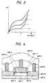
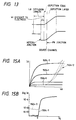
- Fig. 28 solid lines show the results of measurement of the Vd-Id characteristics of the MIS field effect transistor produced under the above-described conditions. It was confirmed from the measurement that the source-drain voltage is 20 V or more and is significantly increased.
- the broken lines in Fig. 28 show the characteristics of a field effect transistor having the source and channel portions with the same energy band gap. The field effect transistor exhibits excellent saturation characteristics at about 5 volt.
- a gate insulating film 1203-4 of 500 ⁇ was then formed by thermal oxidation at 900°C for 30 minutes, and a polycrystal Si was deposited to 4000 ⁇ by the LP-CVD process.
- a P-type polycrystalline Si gate electrode 1203-5 was formed by photolithography (Fig. 14B).
- Ge ions were then injected by using as a mask material the side wall 1203-7 and the gage electrode 1203-5.
- the conditions of the ion injection were an injection energy of 130 KeV and a dose of 1E + 17 cm ⁇ 3. Heat treatment was then performed at 950°C for 30 minutes to form source and drain regions 1203-8 made of SiGe as a second semiconductor material.
- PSG phosphorous glass
- a device was formed by using a ZMR (Zone Melting Recrystalization) wafer comprising an Si layer of 4000 ⁇ and ground SiO2 layer of 1 ⁇ m according to the same production process as that employed in Embodiment 1.
- the conditions of ion injection in the source and drain regions were an energy of 60 KeV and a dose of 2E + 15 cm ⁇ 2
- the conditions of Ge ion injection for forming the second semiconductor material were an energy of 130 KeV and a dose of 2E + 17 cm ⁇ 2.
- a general thin film SOI-MIS transistor containing no Ge ions was formed by the same production method and compared with the transistor of this embodiment.
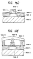
- a polycrystalline silicon gate electrode 1606-5 was then formed on the film 1606-4 so as to be offset from the SiGe:Si heterojunction face by about 0.5 ⁇ m. Impurities were introduced into the source and drain regions by using as a mask material the polycrystalline silicon under the same injection conditions as those in the above-described embodiments to form first semiconductor material portions 1606-6 (Fig. 16D).
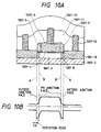
- Fig. 17 is a sectional view showing the prodcution process in this embodiment. Because Fig. 10A is the same as Fig. 17G, this embodiment is described below with reference to the production process of this embodiment shown in Fig. 17.
- a mixed crystal Si x Ge 1-x 1703-10 was then selectively deposited to a thickness of about 500 ⁇ on the silicon layer 1703-8 exposed in the source and drain regions by using a gas mixture SiH4/GeH.
- the deposited portion comprised silicon, and the non-deposited portion comprised a silicon oxide film and a silicon nitride film.
- the mixed crystal rate x was 0.1
- PSG phosphorous glass
- Wiring Al 1703-12 was deposited by the sputtering process.
- PSG was finally deposited to 8000 ⁇ to form a protective film 1703-13 and then subjected to heat treatment at 400°C for 30 minutes (Fig. 17G).
- Fig. 10B is a drawing showing the energy band of the transistor.
- character A denotes the heterojunction faces
- character B denotes the PN junction faces, the region between the junction faces A and B being a high-concentration impurity regions comprising the same semiconductor as that of the channel region.
- the heterojunction faces A comprise a semiconductor having a narrow energy band gap.
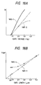
- Fig. 18B shows the dependency of the driving force Gm on the gate length.
- curve 1805-3 shows the results of this embodiment
- curve 1805-4 shows the results of a thin film SOI-MOS transistor containing heterojunctions.
- the transistor shown by curve 1805-4 has the tendency that the driving force Gm is deviated from an ideal straight line as the gate length is decreased because the parasitic resistance of the source and drain regions is made significant, as compared with the on resistance.
- the transistor of this embodiment shown by curve 1805-3 shows the driving force Gm along the ideal line up to a gate length of about 0.8 ⁇ m.
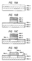
- First ion implantation was performed by using as a mask material the gate electrode 1904-5 for introducing impurities into the source and drain regions 1904-8 (Fig. 19C).
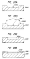
- a seventh embodiment of the present invention is described below with reference to Fig. 20.
- a concave portion of 800 ⁇ deep was formed in a portion on a quartz substrate 2008-1 on which MOSFET is formed later.
- the concave portion had a size of 40 x 40 ⁇ m.
- a polycrystalline silicon region of 2 ⁇ m square was formed at the center of the concave portion. Heat treatment was then performed in an atmosphere of H2 to change the polycrystalline silicon region to a single crystal silicon region 2008-2 by aggregation (Fig. 20A).
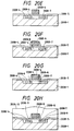
- a silicon oxide film 2008-5 was deposited as a gate oxide film on the substrate by the CVD process (Fig. 20D).
- Polycrystalline silicon was then deposited to 4000 ⁇ by the CVD process to form a gate electrode 2008-6.
- Impurities were introduced by ion implantation using as a mask the gate electrode 2008-6 to form source and drain regions 2008-7 (Fig. 20E).
- a silicon oxide film was then deposited by the CVD process for forming a side wall.
- Anisotropic etching was then performed to form a side wall 2008-8 having a thickness of about 1000 ⁇ (Fig. 20F).
- the channel region 2008-4 and the source and drain regions 2008-7 had the following structure:
- the diffusion length L d of Si 0.1 Ge 0.9 which formed the regions 2008-4 and 2008-7 was about 1 ⁇ m which is longer than the above distance 1000 ⁇ .
- the field effect mobility was as high as about 1200 cm2/v ⁇ s, but a good linear region was obtained in the Id-Vg characteristics.
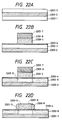
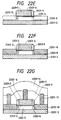
- Al-Si 2203-10 was selectively deposited to about 500 ⁇ by a lamp overheating method under a gas mixture containing monomethylaluminum as a raw material gas and H2 gas as reaction gas at a substrate surface temperature of 350°C to form a metal electrode for the source and drain regions only on the silicon portion 2203-8 which was exposed to the source and drain regions.
- the deposited portion comprised a silicon material
- the non-deposited portion comprised a silicon oxide film and a silicon nitride film.
- the metal electrodes 2203-10 for the source and drain were placed within a diffusion length L d of about 1 ⁇ m from the depletion edges of the PN junctions (Fig. 22F).
- Fig. 21B is a drawing showing the energy band of the transistor of this embodiment.
- character A denotes heterojunction faces
- character B denotes PN junction faces, high-concentration impurity regions being held between the junction faces A and B.
- the metal electrode 2203-10 is present from a turn at the face A where no forbidden band region such as a semiconductor region is present.
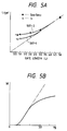
- Fig. 23 is a drawing showing the device characteristics of this embodiment.
- Fig. 23A is a drawing showing the Id-Vg characteristics in which reference numeral 2304-1 shows this embodiment, and reference numeral 2304-2 shows a comparative example of thin film SOI-MOS transistors.
- reference numeral 2304-1 shows this embodiment
- reference numeral 2304-2 shows a comparative example of thin film SOI-MOS transistors.
- the metal electrodes in the source and drain regions are extremely close to the source-channel junction edges, as compared with the source-drain electrodes in a conventional transistor, the parasitic resistance is very low, and a good linearity is thus obtained.
- the driving force (the slopes of the courves shown in the drawing) is increased about twice.
- Fig. 23B is a drawing showing the dependency of the driving force to the gate length.
- curve 2304-3 shows the results of this embodiment
- curve 2304-4 shows the results of a thin film SOI-MOS transistor used for comparison.
- the comparative example shows a deviation from the ideal line (the one-dot chain line shown in the drawing) as the gate length decreases. This represents that the parasitic resistance in the source and drain portions becomes significant, as compared with the on resistance.
- the transistor of this embodiment shows the dependency along the ideal line up to a gate length of about 0.8 ⁇ m. This shows that the parasitic resistance is sufficiently low.
- Fig. 23C is a drawing showing the Id-Vg characteristics.
- curve 2304-5 shows the results of this embodiment
- curve 2304-6 shows the results of a thin film SOI-MOS transistor used for comparison.
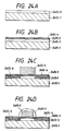
- a SOI substrate having a semiconductor layer with a thickness of 500 ⁇ was formed (Fig. 24A).
- a silicon oxide film 2405-3 having a thickness of 300 ⁇ was then formed on the substrate by the thermal oxidation method, and Si3M4 2405-4 was deposited to 200 ⁇ on the oxide film 2405-3 by the LP-CVD process to form a two-layer gate insulating film (Fig. 24B).
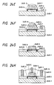
- Polycrystalline silicon was then deposited to 5000 ⁇ by the LP-CVD process to form a gate electrode 2405-5.
- the spacer 2405-7 was then subjected to dry etching so as to have the sectional structure shown in Fig. 24E (Fig. 24E).
- WSi (tungsten silicide) 2405-8 was then deposited over the whole surface by the sputtering process (Fig. 24F).
- An inter layer insulating film 2405-9, metal wiring (WSi) 2405-10 and a protective fime were then formed by the same method as that employed in the seventh embodiment.
- a MOS transistor having metal electrodes 2405-8 which were provided within the diffusion length L d from the PN junction faces and which were extended to the quartz substrate 2405-1 having the ground insulating film was formed (Fig. 24H).
- the SOI-MOS transistor of this embodiment showed no kink phenomenon and had a source-drain endurance voltage of 20 V or more and the Id-Vg characteristics with good linearity.
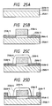
- Fig. 25A polycrystalline silicon was deposited on a quartz substrate 2506-1 by the LP-CVD process and then molten and recrystallized by applying an eximer laser thereto to form a semiconductor silicon layer 2506-2.
- the thickness of the semiconductor layer was adjusted by sacrifice oxidation.
- a SOI substrate having the semiconductor silicon layer 2506-2 having a thickness of 500 ⁇ was thus formed.
- 200 ⁇ gate oxide film 2506-3 having a thickness of 200 ⁇ was then formed by the thermal oxidation method (Fig. 25A).
- a polycrystalline silicon film was then deposited to 4000 ⁇ by the LP-CVD process to form a gate electrode 2506-4, and impurities were introduced into source and drain regions 2506-5 by ion implantation using as a mask the gate electrode 2506-4 (Fig. 25B).
- the polycrystalline silicon which formed the gate electrode 2506-4 was then thermally oxidized to form a polycrystalline silicon oxide film 2506-6 having a thickness of 2000 ⁇ (Fig. 25C).
- a resist 2506-7 was then applied for forming contact holes, as shown in Fig. 25D (Fig. 25D).
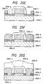
- the contact holes were formed with self alignment. In this formation, the contact holes could be formed with self alignment without being short-circuited with the gate electrode by etching the oxide film in an amount of 400 ⁇ (Fig. 25E).
- the source-drain metal electrodes 2506-8 are disposed within the diffusion length of 1 ⁇ m from the source-channel PN junction faces, and the metal electrodes 2506-8 are extended to the ground quartz substrate 2506-1.
- a PSG film was then deposited to 8000 ⁇ to form a protective film.
- a recrystallized silicon thin film SOI-MOS transistor was formed by the same method as that employed in this embodiment with the exception that a metal electrode was formed of AlSi, and the temperature of heat treatment after the metal electrode was deposited was 400°C and compared with the transistor of this embodiment. As a result, it was found that the transistor of this embodiment has an improved endurance voltage and Id-Vg characteristics with a good linear region.
- the energy band gap Eg2 in the source portion is set to a value different from the energy band gap Eg1 in the channel portion, holes are smoothly moved between the source and channel, and good saturation properties and a high source-drain endurance voltage can be obtained.
- the MIS transistor of the present invention produces no phenomenon that the dark current is increased due to the generation of the current from defects which serve as generation sources or paths (for example, hopping current), as in a conventional transistor in which the source-channel PN junctions are heterojunctions, or heterojunctions are included in the depletion layers of the PN junctions.
- a thin film SOI-MIS transistor formed by using as a semiconductor material a mixed crystal of silicon and germanium and having a heterojunction provided at least in a source region is characterized by the following:
- the invention also has the effects of preventing the kink phenomenon and increasing the source-drain endurance voltage.
- a metal electrode of a source portion is provided within the diffusion length L d from the source-side depletion edge of the source-channel PN junction and is extended to the ground insulating film, thereby improving the resistance to the kink phenomenon and the source-drain endurance voltage, significantly decreasing the parasitic resistance of the source and drain portions and preventing the deterioration in the driving force.
- An MIS field effect transistor is provided with a first conduction type semiconductor layer having a channel portion, a second conduction type impurity region which forms opposite source and drain portion with the channel portion therebetween, and a gate electrode provided on the channel portion with a gate insulating film therebetween, wherein the channel and source portions respectively consist of semiconductors having different energy band gaps.
- the transistor enables holes to be smoothly moved between the source and channel portions, and has good saturation properties and a high source-drain endurance voltage.
Landscapes
- Thin Film Transistor (AREA)
- Semiconductor Memories (AREA)
Claims (11)
- Un transistor MIS comprenant une partie canal (409-3) formée sur un substrat isolant (409-2) en utilisant un premier type de conduction d'un premier matériau semi-conducteur, des parties source et drain d'un deuxième type de conduction (409-8, 409-10) comprenant ladite partie canal (409-3) entre elles, et une électrode de gâchette (409-5) formée sur une surface principale de ladite partie canal (409-3) avec un film isolant (409-4) entre elles, ledit transistor MIS étant caractérisé par le fait que ladite partie source (409-8, 409-10) est faite dudit premier matériau semi-conducteur (409-8) et d'un deuxième matériau semiconducteur (409-10) ayant un intervalle de bande d'énergie plus petit que celui dudit premier matériau semi-conducteur ; et une jonction hétérogène entre lesdits premier et deuxième matériaux semi-conducteurs est appliquée en dehors de la région de la couche de déplétion formée dans la jonction PN entre lesdites parties source (409-8) et canal (409-3) et à l'intérieur d'une longueur de diffusion Ld à partir du bord de déplétion.
- Un transistor MIS conforme à la revendication 1, caractérisé par le fait que ledit bord de déplétion est essentiellement placé au niveau de la face de la jonction PN entre lesdites parties source (409-8) et canal (409-3).
- Un transistor MIS conforme à la revendication 1, caractérisé par le fait que ledit premier matériau semi-conducteur est du silicium et que le deuxième matériau semi-conducteur est une solution solide de silicium et de germanium.
- Un transistor MIS conforme à la revendication 1, caractérisé par le fait que lesdits premier et deuxième matériaux semi-conducteurs sont des semi-conducteurs composites.
- Un transistor MIS conforme à la revendication 4, caractérisé par le fait que ledit semi-conducteur composite utilisé en tant que ledit premier matériau semi-conducteur est du GaAs1-xSbx, et ledit semi-conducteur composite utilisé en tant que ledit deuxième matériau semi-conducteur est du GaAs1-ySby avec x < y.
- Un transistor MIS conforme à la revendication 1, caractérisé par le fait que ledit deuxième matériau semi-conducteur est formé par l'introduction, dans ledit premier matériau semi-conducteur, d'un atome différent de celui dudit premier matériau semi-conducteur par implantation ionique.
- Un transistor MIS conforme à la revendication 1, caractérisé par le fait qu'au moins ladite partie source (409-8) présente une face de jonction hétérogène et contient en tant que ledit deuxième matériau semi-conducteur une région de solution solide composée de silicium avec un taux de solution solide x et du germanium, et ladite partie canal (409-3) contient en tant que ledit matériau semi-conducteur du premier type de conduction une solution solide composée de silicium avec un taux de solution solide y et du germanium, et lesdits taux de solution solide x et y satisfont aux conditions que x < y et x < 0,12.
- Un transistor MIS conforme à la revendication 7, caractérisé par le fait que ladite face de la jonction hétérogène n'est pas incluse dans la couche de déplétion formée dans ladite jonction PN et est appliquée à l'intérieur d'une longueur de diffusion Ld à partir du bord de déplétion de ladite jonction PN.
- Un transistor MIS comprenant une partie canal (2203-3) formée sur un substrat isolant (2203-2) en utilisant un premier type de conduction d'un premier matériau semi-conducteur, des parties source et drain (2203-8, 2203-10) d'un deuxième type de conduction ayant ladite partie canal disposée entre elles, et une électrode de gâchette (2203-5) formée sur une surface principale de ladite partie canal (2203-3) avec un film isolant (2203-4) disposé entre elles, ledit transistor MIS étant caractérisé par le fait que lesdites parties source et drain (2203-8, 2203-10) sont faites dudit premier matériau semi-conducteur (2203-8) et d'une électrode métallique (2203-10), et qu'au moins ladite électrode métallique (2203-10) de ladite partie source est présente à l'extérieur de la région de la couche de déplétion de la jonction PN entre ledit canal (2203-3) et les parties source et drain (2203-8) et à l'intérieur d'une longueur de diffusion Ld à partir du bord de déplétion des parties source et drain (2203-8) du côté source.
- Un transistor MIS conforme à la revendication 9, caractérisé par le fait que ladite électrode métallique (2203-10) d'au moins ladite partie source est étendue audit substrat isolant (2203-2).
- Un transistor MIS conforme à la revendication 9, caractérisé par le fait que lesdites électrodes métalliques (2203-10) sont faites d'aluminium, et qu'un traitement thermique est réalisé sensiblement à 470 °C après que lesdites électrodes métalliques (2203-10) ont été formées.
Applications Claiming Priority (8)
| Application Number | Priority Date | Filing Date | Title |
|---|---|---|---|
| JP292120/90 | 1990-10-31 | ||
| JP29212090 | 1990-10-31 | ||
| JP292121/90 | 1990-10-31 | ||
| JP29211990 | 1990-10-31 | ||
| JP29212190 | 1990-10-31 | ||
| JP292119/90 | 1990-10-31 | ||
| JP21451/91 | 1991-01-23 | ||
| JP2145191 | 1991-01-23 |
Publications (2)
| Publication Number | Publication Date |
|---|---|
| EP0483824A1 EP0483824A1 (fr) | 1992-05-06 |
| EP0483824B1 true EP0483824B1 (fr) | 1995-10-04 |
Family
ID=27457583
Family Applications (1)
| Application Number | Title | Priority Date | Filing Date |
|---|---|---|---|
| EP91118558A Expired - Lifetime EP0483824B1 (fr) | 1990-10-31 | 1991-10-30 | Transistor MIS avec hétérojunction |
Country Status (5)
| Country | Link |
|---|---|
| US (1) | US5475244A (fr) |
| EP (1) | EP0483824B1 (fr) |
| JP (1) | JP2947654B2 (fr) |
| CA (1) | CA2054498C (fr) |
| DE (1) | DE69113571T2 (fr) |
Families Citing this family (23)
| Publication number | Priority date | Publication date | Assignee | Title |
|---|---|---|---|---|
| JP3437863B2 (ja) | 1993-01-18 | 2003-08-18 | 株式会社半導体エネルギー研究所 | Mis型半導体装置の作製方法 |
| US5728592A (en) * | 1992-10-09 | 1998-03-17 | Fujitsu Ltd. | Method for fabricating a thin film transistor matrix device |
| JPH06310719A (ja) * | 1993-04-19 | 1994-11-04 | Sharp Corp | Ge−SiのSOI型MOSトランジスタ及びその製造方法 |
| US5581092A (en) * | 1993-09-07 | 1996-12-03 | Semiconductor Energy Laboratory Co., Ltd. | Gate insulated semiconductor device |
| TW297142B (fr) * | 1993-09-20 | 1997-02-01 | Handotai Energy Kenkyusho Kk | |
| US6777763B1 (en) | 1993-10-01 | 2004-08-17 | Semiconductor Energy Laboratory Co., Ltd. | Semiconductor device and method for fabricating the same |
| JP3030368B2 (ja) | 1993-10-01 | 2000-04-10 | 株式会社半導体エネルギー研究所 | 半導体装置およびその作製方法 |
| KR0135804B1 (ko) * | 1994-06-13 | 1998-04-24 | 김광호 | 실리콘 온 인슐레이터(soi) 트랜지스터 |
| JP3361922B2 (ja) * | 1994-09-13 | 2003-01-07 | 株式会社東芝 | 半導体装置 |
| JP3243146B2 (ja) | 1994-12-08 | 2002-01-07 | 株式会社東芝 | 半導体装置 |
| US5773328A (en) * | 1995-02-28 | 1998-06-30 | Sgs-Thomson Microelectronics, Inc. | Method of making a fully-dielectric-isolated fet |
| US6870232B1 (en) * | 1996-07-18 | 2005-03-22 | International Business Machines Corporation | Scalable MOS field effect transistor |
| JPH1140811A (ja) | 1997-07-22 | 1999-02-12 | Hitachi Ltd | 半導体装置およびその製造方法 |
| US6060749A (en) * | 1998-04-23 | 2000-05-09 | Texas Instruments - Acer Incorporated | Ultra-short channel elevated S/D MOSFETS formed on an ultra-thin SOI substrate |
| US6124627A (en) * | 1998-12-03 | 2000-09-26 | Texas Instruments Incorporated | Lateral MOSFET having a barrier between the source/drain region and the channel region using a heterostructure raised source/drain region |
| US6621131B2 (en) * | 2001-11-01 | 2003-09-16 | Intel Corporation | Semiconductor transistor having a stressed channel |
| US7262105B2 (en) * | 2003-11-21 | 2007-08-28 | Freescale Semiconductor, Inc. | Semiconductor device with silicided source/drains |
| FR2868207B1 (fr) * | 2004-03-25 | 2006-09-08 | Commissariat Energie Atomique | Transistor a effet de champ a materiaux de source, de drain et de canal adaptes et circuit integre comportant un tel transistor |
| US7825400B2 (en) * | 2006-06-09 | 2010-11-02 | Intel Corporation | Strain-inducing semiconductor regions |
| JP2009054719A (ja) * | 2007-08-24 | 2009-03-12 | Tokyo Electron Ltd | 半導体製造方法、半導体製造装置および表示装置 |
| US7750368B2 (en) * | 2008-06-13 | 2010-07-06 | Macronix International Co., Ltd. | Memory device |
| US9818744B2 (en) * | 2014-09-04 | 2017-11-14 | Taiwan Semiconductor Manufacturing Company, Ltd. | Leakage current suppression methods and related structures |
| CN121040234A (zh) * | 2024-03-28 | 2025-11-28 | 京东方科技集团股份有限公司 | 晶体管、驱动背板及制备方法和显示装置 |
Family Cites Families (16)
| Publication number | Priority date | Publication date | Assignee | Title |
|---|---|---|---|---|
| JPS59231865A (ja) * | 1983-06-14 | 1984-12-26 | Seiko Epson Corp | 半導体装置 |
| JPS60224274A (ja) * | 1984-04-20 | 1985-11-08 | Nec Corp | 絶縁基板mis型電界効果トランジスタの製造方法 |
| US4673957A (en) * | 1984-05-14 | 1987-06-16 | Energy Conversion Devices, Inc. | Integrated circuit compatible thin film field effect transistor and method of making same |
| US4727044A (en) * | 1984-05-18 | 1988-02-23 | Semiconductor Energy Laboratory Co., Ltd. | Method of making a thin film transistor with laser recrystallized source and drain |
| JPS6156460A (ja) * | 1984-08-28 | 1986-03-22 | Nec Corp | 半導体装置及びその製造方法 |
| US4603471A (en) * | 1984-09-06 | 1986-08-05 | Fairchild Semiconductor Corporation | Method for making a CMOS circuit having a reduced tendency to latch by controlling the band-gap of source and drain regions |
| JPS62131573A (ja) * | 1985-12-04 | 1987-06-13 | Hitachi Ltd | 半導体装置 |
| JPS63252478A (ja) * | 1987-04-09 | 1988-10-19 | Seiko Instr & Electronics Ltd | 絶縁ゲ−ト型半導体装置 |
| GB2211022B (en) * | 1987-10-09 | 1991-10-09 | Marconi Electronic Devices | A semiconductor device and a process for making the device |
| JP2841419B2 (ja) * | 1988-02-19 | 1998-12-24 | 株式会社デンソー | 多結晶ダイオードおよびその製造方法 |
| US5142641A (en) * | 1988-03-23 | 1992-08-25 | Fujitsu Limited | CMOS structure for eliminating latch-up of parasitic thyristor |
| JPH01248668A (ja) * | 1988-03-30 | 1989-10-04 | Seiko Epson Corp | 薄膜トランジスタ |
| JPH01276765A (ja) * | 1988-04-28 | 1989-11-07 | Seiko Epson Corp | 薄膜トランジスタ |
| JPH02188967A (ja) * | 1989-01-18 | 1990-07-25 | Nissan Motor Co Ltd | 半導体装置 |
| JP2698182B2 (ja) * | 1989-07-31 | 1998-01-19 | 三洋電機株式会社 | 薄膜トランジスタ |
| JP2888878B2 (ja) * | 1989-10-02 | 1999-05-10 | 株式会社東芝 | 半導体装置 |
-
1991
- 1991-10-25 JP JP30571291A patent/JP2947654B2/ja not_active Expired - Fee Related
- 1991-10-30 EP EP91118558A patent/EP0483824B1/fr not_active Expired - Lifetime
- 1991-10-30 CA CA002054498A patent/CA2054498C/fr not_active Expired - Fee Related
- 1991-10-30 DE DE69113571T patent/DE69113571T2/de not_active Expired - Fee Related
-
1993
- 1993-03-24 US US08/037,681 patent/US5475244A/en not_active Expired - Fee Related
Also Published As
| Publication number | Publication date |
|---|---|
| JPH053322A (ja) | 1993-01-08 |
| EP0483824A1 (fr) | 1992-05-06 |
| DE69113571D1 (de) | 1995-11-09 |
| JP2947654B2 (ja) | 1999-09-13 |
| DE69113571T2 (de) | 1996-03-28 |
| US5475244A (en) | 1995-12-12 |
| CA2054498A1 (fr) | 1992-05-01 |
| CA2054498C (fr) | 1997-05-20 |
Similar Documents
| Publication | Publication Date | Title |
|---|---|---|
| EP0483824B1 (fr) | Transistor MIS avec hétérojunction | |
| KR100647173B1 (ko) | 혁신적인 전계 효과 트랜지스터와 제조방법 | |
| CA2058513C (fr) | Transistor soi en couches minces et sa methode de fabrication | |
| US6475869B1 (en) | Method of forming a double gate transistor having an epitaxial silicon/germanium channel region | |
| JP3260660B2 (ja) | 半導体装置およびその製造方法 | |
| EP0684650B1 (fr) | Dispositif semi-conducteur à couche mince avec structure d'une couche de SiGe et sa méthode de fabrication | |
| US20050161711A1 (en) | High performance FET devices and methods thereof | |
| US20080237655A1 (en) | Semiconductor apparatus and method for manufacturing same | |
| US6461945B1 (en) | Solid phase epitaxy process for manufacturing transistors having silicon/germanium channel regions | |
| US20100013015A1 (en) | Metal source/drain schottky barrier silicon-on-nothing mosfet device | |
| US20090014794A1 (en) | Mosfet with laterally graded channel region and method for manufacturing same | |
| JPH05283691A (ja) | 薄膜トランジスタ及びその製造方法 | |
| JP3383154B2 (ja) | 半導体装置 | |
| US6743680B1 (en) | Process for manufacturing transistors having silicon/germanium channel regions | |
| US7316959B2 (en) | Semiconductor device and method for fabricating the same | |
| Lee et al. | A high-performance polycrystalline silicon thin film transistor with a silicon nitride gate insulator | |
| US7612421B2 (en) | Electronic device with dopant diffusion barrier and tunable work function and methods of making same | |
| JPH0575127A (ja) | 薄膜半導体装置 | |
| KR20070040128A (ko) | 박막 트랜지스터 및 그 제조방법 | |
| JP2007158300A (ja) | 低いショットキー障壁貫通トランジスタ及びその製造方法 | |
| Chang et al. | A novel germanium doping method for fabrication of high-performance p-channel poly-Si 1-x Ge x TFT by excimer laser crystallization | |
| JPH0637103A (ja) | バイポーラトランジスタおよびその製法 | |
| JPH065860A (ja) | 薄膜トランジスタ及びその製造方法 | |
| JPH05326964A (ja) | Mosトランジスタ | |
| JPH06204478A (ja) | Mos型薄膜トランジスタ |
Legal Events
| Date | Code | Title | Description |
|---|---|---|---|
| PUAI | Public reference made under article 153(3) epc to a published international application that has entered the european phase |
Free format text: ORIGINAL CODE: 0009012 |
|
| AK | Designated contracting states |
Kind code of ref document: A1 Designated state(s): DE FR GB IT NL |
|
| 17P | Request for examination filed |
Effective date: 19920922 |
|
| 17Q | First examination report despatched |
Effective date: 19940421 |
|
| GRAA | (expected) grant |
Free format text: ORIGINAL CODE: 0009210 |
|
| AK | Designated contracting states |
Kind code of ref document: B1 Designated state(s): DE FR GB IT NL |
|
| REF | Corresponds to: |
Ref document number: 69113571 Country of ref document: DE Date of ref document: 19951109 |
|
| ET | Fr: translation filed | ||
| ITF | It: translation for a ep patent filed | ||
| PLBE | No opposition filed within time limit |
Free format text: ORIGINAL CODE: 0009261 |
|
| STAA | Information on the status of an ep patent application or granted ep patent |
Free format text: STATUS: NO OPPOSITION FILED WITHIN TIME LIMIT |
|
| 26N | No opposition filed | ||
| REG | Reference to a national code |
Ref country code: GB Ref legal event code: IF02 |
|
| PGFP | Annual fee paid to national office [announced via postgrant information from national office to epo] |
Ref country code: FR Payment date: 20051010 Year of fee payment: 15 |
|
| PGFP | Annual fee paid to national office [announced via postgrant information from national office to epo] |
Ref country code: NL Payment date: 20051016 Year of fee payment: 15 |
|
| PGFP | Annual fee paid to national office [announced via postgrant information from national office to epo] |
Ref country code: GB Payment date: 20051026 Year of fee payment: 15 |
|
| PGFP | Annual fee paid to national office [announced via postgrant information from national office to epo] |
Ref country code: DE Payment date: 20051027 Year of fee payment: 15 |
|
| PGFP | Annual fee paid to national office [announced via postgrant information from national office to epo] |
Ref country code: IT Payment date: 20061031 Year of fee payment: 16 |
|
| PG25 | Lapsed in a contracting state [announced via postgrant information from national office to epo] |
Ref country code: DE Free format text: LAPSE BECAUSE OF NON-PAYMENT OF DUE FEES Effective date: 20070501 Ref country code: NL Free format text: LAPSE BECAUSE OF NON-PAYMENT OF DUE FEES Effective date: 20070501 |
|
| GBPC | Gb: european patent ceased through non-payment of renewal fee |
Effective date: 20061030 |
|
| NLV4 | Nl: lapsed or anulled due to non-payment of the annual fee |
Effective date: 20070501 |
|
| REG | Reference to a national code |
Ref country code: FR Ref legal event code: ST Effective date: 20070629 |
|
| PG25 | Lapsed in a contracting state [announced via postgrant information from national office to epo] |
Ref country code: GB Free format text: LAPSE BECAUSE OF NON-PAYMENT OF DUE FEES Effective date: 20061030 |
|
| PG25 | Lapsed in a contracting state [announced via postgrant information from national office to epo] |
Ref country code: FR Free format text: LAPSE BECAUSE OF NON-PAYMENT OF DUE FEES Effective date: 20061031 |
|
| PG25 | Lapsed in a contracting state [announced via postgrant information from national office to epo] |
Ref country code: IT Free format text: LAPSE BECAUSE OF NON-PAYMENT OF DUE FEES Effective date: 20071030 |