EP0483866A2 - Signalverarbeitungsvorrichtung - Google Patents
Signalverarbeitungsvorrichtung Download PDFInfo
- Publication number
- EP0483866A2 EP0483866A2 EP91118650A EP91118650A EP0483866A2 EP 0483866 A2 EP0483866 A2 EP 0483866A2 EP 91118650 A EP91118650 A EP 91118650A EP 91118650 A EP91118650 A EP 91118650A EP 0483866 A2 EP0483866 A2 EP 0483866A2
- Authority
- EP
- European Patent Office
- Prior art keywords
- signal
- balanced
- color
- output
- modulator
- Prior art date
- Legal status (The legal status is an assumption and is not a legal conclusion. Google has not performed a legal analysis and makes no representation as to the accuracy of the status listed.)
- Granted
Links
Images


Classifications
-
- H—ELECTRICITY
- H04—ELECTRIC COMMUNICATION TECHNIQUE
- H04N—PICTORIAL COMMUNICATION, e.g. TELEVISION
- H04N9/00—Details of colour television systems
- H04N9/64—Circuits for processing colour signals
- H04N9/65—Circuits for processing colour signals for synchronous modulators
-
- H—ELECTRICITY
- H04—ELECTRIC COMMUNICATION TECHNIQUE
- H04N—PICTORIAL COMMUNICATION, e.g. TELEVISION
- H04N1/00—Scanning, transmission or reproduction of documents or the like, e.g. facsimile transmission; Details thereof
- H04N1/46—Colour picture communication systems
- H04N1/64—Systems for the transmission or the storage of the colour picture signal; Details therefor, e.g. coding or decoding means therefor
- H04N1/646—Transmitting or storing colour television type signals, e.g. PAL, Lab; Their conversion into additive or subtractive colour signals or vice versa therefor
-
- H—ELECTRICITY
- H04—ELECTRIC COMMUNICATION TECHNIQUE
- H04N—PICTORIAL COMMUNICATION, e.g. TELEVISION
- H04N9/00—Details of colour television systems
- H04N9/79—Processing of colour television signals in connection with recording
- H04N9/80—Transformation of the television signal for recording, e.g. modulation, frequency changing; Inverse transformation for playback
- H04N9/81—Transformation of the television signal for recording, e.g. modulation, frequency changing; Inverse transformation for playback the individual colour picture signal components being recorded sequentially only
Definitions
- This invention relates to a signal processing device which is arranged to process an information signal.
- An electronic still video system has been known as one of information signal processing devices.
- the electronic still video system is arranged as follows: A luminance component of a color still image signal is frequency-modulated. Two color-difference signals which are included in the color still image signal as a chrominance component are frequency-modulated after they are processed into a color-difference line-sequential signal. The frequency-modulated luminance signal and the frequency-modulated color-difference line-sequential signal thus obtained are frequency-multiplexed into a recording image signal to be recorded on a magnetic disc. The recording image signal recorded on the magnetic disc is reproduced. From the reproduced signal, the frequency-modulated luminance signal and the frequency-modulated color-difference line-sequential signal are separated. These separated signals are frequency-demodulated.
- the color-difference line-sequential signal is restored to the two color-difference signals by converting the line-sequential state into a coincident state.
- the two color-difference signals are further converted into a chrominance signal by quadrature two-phase modulation.
- the chrominance signal thus obtained is frequency-multiplexed with the frequency-demodulated luminance signal to obtain and output a TV signal from the electronic still video system.
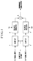
- Fig. 1 of the accompanying drawings shows in outline and in part the arrangement of a signal processing circuit included in the reproducing apparatus of the above-stated electronic still video system.
- the circuit shown in Fig. 1 represents a chrominance color encoder which is arranged to convert the two kinds of color-difference signals into a chrominance signal by using balanced modulators.
- a color-difference signal R-Y is inputted to a clamp circuit 1 and a color-difference signal B-Y to a clamp circuit 3. These signals R-Y and B-Y are clamped for a period of time designated by clamp pulse signals CLP which are inputted respectively to the clamp circuits 1 and 3.
- the signal R-Y is supplied to a balanced modulator 2 and the signal B-Y to a balanced modulator 4.
- a modulation carrier signal fsc1 is supplied to the balanced modulator 2 and a modulation carrier signal fsc2 to the balanced modulator 4.
- Each of these balanced modulators 2 and 4 is arranged to perform a balanced modulating process on the signal R-Y or the signal B-Y with the modulation carrier signal fsc1 or fsc2.
- the outputs of the balanced modulators 2 and 4 are supplied to an adder 5.
- both the modulation carrier signals fsc1 and fsc2 are arranged to be at a frequency 3.58 MHz.
- the phase of the carrier signal fsc1 is then arranged to be at 90 o while that of the other carrier signal fsc2 is at 0 o .
- a chrominance signal is formed by adding together the signals supplied from the balanced modulators 2 and 4. The chrominance signal thus formed is outputted from the adder 5.
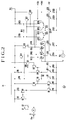
- Fig. 2 is a circuit diagram showing in part the circuit arrangement of the color encoder shown in Fig. 1.
- the circuit of Fig. 2 corresponds to the clamp circuit 1 and the balanced modulator 2 or to the clamp circuit 3 and the balanced modulator 4 shown in Fig. 1.
- Figs. 3(a) to 3(i) and 4(a) to 4(j) show, in timing charts, signal waveforms obtained from the various parts of the circuit shown in Fig. 2. The operation of the circuit shown in Fig. 2 is described below with reference to Figs. 3(a) to 3(i) and 4(a) to 4(j):
- a clamp circuit is formed with transistors Q1 to Q5, resistors R2 to R4 and a capacitor C1.
- a clamp pulse signal CLP which is as shown at Fig. 4(i) is inputted to the base of the transistor Q5.
- K1 represents a constant, Vcc a power supply voltage and VBE a voltage between the base and the emitter of the transistor Q5
- K1 represents a constant, Vcc a power supply voltage and VBE a voltage between the base and the emitter of the transistor Q5
- a constant current flows to an analog switch which consists of transistors Q1 and Q2 through a current mirror circuit which consists of resistors Q3 and Q4.
- the constant current is thus applied to the analog switch during the high-level period of the clamp pulse signal CLP.
- the DC potential of the color encoder is thus fixed at a bias potential V1.
- a clamping action is performed to fix at above-stated bias potential V1 the blanking level of the color-difference signal which is inputted from a terminal VIN in a state as shown in Fig. 4(b).
- the color-difference signal which has been subjected to the above-stated clamping action is supplied to the base of a transistor Q6 which forms a buffer circuit.
- the output of the transistor Q6 is inputted to a differential amplifier which consists of transistors Q8 and Q10.
- the output of the differential amplifier is inputted to the balanced modulator as two differential output signals.
- a circuit which is composed of transistors Q31, Q12 and Q13 and resistors R26 and R11 is arranged to form another reference voltage input (a blanking level) for the differential amplifier.
- the base of the transistor 31 of this circuit is caused to be constantly in a saturated state by the resistor 26 and to have a saturation voltage between the collector and the emitter thereof, because:
- the clamping analog switch which is formed by the transistors Q1 and Q2 is also in a saturated state like the transistor Q31 during the clamping process of the clamping analog switch, i.e., during the blanking period and, the base voltage of the transistor Q6 is not at the bias potential V1 and is higher than the bias voltage V1 by as much as the saturation voltages of the transistors Q1 and Q2.
- the constant saturated state of the base of the transistor Q31 is thus arranged to permit compensation for the higher portion of the base voltage of the transistor Q6. This compensation can be made by suitably adjusting the value of the resistor R26.
- K2 ⁇ Vcc + VBE (wherein K2 represents a constant, Vcc the power supply voltage and VBE a voltage between the base and the emitter of the transistor to be connected) is expressed as V2 and that a resistor R5 is equal to a resistor R11, a resistor R7 is equal to a resistor R10 and a resistor R6 is equal to a resistor 9, differential signals obtained by compensating the color-difference signal are inputted to the transistors Q14 and Q18.
- the modulation carrier signal fsc which is as shown in Fig. 3(a) is inputted to the bases of transistors Q15, Q17, Q19 and Q21; and four kinds of signals which are balanced-modulated with the modulation carrier signal fsc and are as shown in Figs. 3(c) to 3(f) are outputted from the collectors of the transistors Q15, Q17, Q19 and Q21, respectively.
- the voltage level of the modulation carrier signal fsc which is included in the signals shown in Figs. 3(c) to 3(f) is determined by currents flowing to resistors R12, R13, R15 and R16.
- the voltage level of the modulation carrier signal fsc is arranged to be set at about 0.2 V with the resistors R12, R13, R15 and R16 assumed to be of equal values.
- Resistors R20 and R22 are arranged to be of equal values, and resistors R18 and R23 are arranged to be of equal valves. With these resistors thus arranged, transistors Q23 and Q25 become operative and transistors Q22 and Q26 inoperative during the high-level period of the modulation carrier signal fsc shown in Fig. 3(a), because:
- the signal outputted from the collector of the transistor Q25 is outputted from an output terminal VO1 as shown in Fig. 2.
- the signal from the collector of the transistor Q23 is outputted from another output terminal VO2. This means that the outputs of a differential amplifier which is formed by the transistors Q23 and Q25 are outputted from the output terminals VO1 and VO2 of Fig. 2.
- the transistors Q22 and Q26 are operative while the transistors Q23 and Q25 are inoperative. Then, the outputs of a differential amplifier which is formed by the transistors Q22 and Q26 are outputted from the output terminals VO1 and VO2.
- the balanced-modulated color-difference signals which are as shown in Figs. 3(g) and 3(h) are not outputted from the output terminals VO1 and VO2 during a period of time A shown in Figs. 3(a) to 3(i), that is, during the blanking period.
- the balanced-modulated color-difference signals are outputted from the output terminals VO1 and VO2 as shown in Figs. 3(g) and 3(h) during a period of time B which is also shown in Figs. 3(a) to 3(i), that is, during a period of having the color-difference components present.
- a circuit arranged in the above-stated manner hardly performs a normal operation if the characteristics of each pair of elements are not matched to each other.
- current density would be changed by unevenness of the areas of the emitters of the transistors resulting from deviations of mask pattern, etc.
- the change in current density then causes an error ⁇ VBE of the voltage between the base and the emitter of each transistor.
- the above-stated error ⁇ VBE also arises if each pair of transistors have uneven characteristics among the transistors Q1 to Q13 and Q31 shown in Fig. 2. If, for example, the DC potential of the color-difference signal supplied to the transistor Q14 is a little higher than that of the color-difference signal supplied to the transistor Q18, the error ⁇ VBE causes the level of normal signal waveforms which are as shown by full lines in Figs. 4(c) and 4(d) to change to signal waveforms which are shown by dotted lines in Figs. 4(c) and 4(d). As a result, modulation carrier components would be generated during the blanking periods A and B, as shown by dotted lines in Figs. 4(g) and 4(h).
- the above-stated phenomenon causes such a color component that should not be generated to appear on a monitor device which is connected to the reproducing apparatus having the circuit of Fig. 2. Further, if the level of the color-difference signal supplied to the circuit described is low, the levels of balanced-modulated color-difference components would vary to cause changes in the hues of the original color components.
- a signal processing device arranged as an embodiment of this invention to process an information signal comprises: a first modulator arranged to modulate an input information signal in accordance with a modulation carrier signal and to output a first output modulated signal; a second modulator arranged to modulate the first output modulated signal outputted from the first modulator in accordance with a modulation carrier signal which is identical to the modulation carrier signal used by the first modulator and to output a second output modulated signal; and an information signal correcting circuit for correcting the information signal being inputted to the first modulator by using the second output modulated signal outputted from the second modulator.
- a further object of the invention is to provide a signal processing device which is capable of forming a good chrominance signal by minimizing signal deterioration in forming the chrominance signal from two kinds of color-difference signals.
- Fig. 1 is a block diagram showing the circuit arrangement of a chrominance color encoder which is a part of the signal processing device of a reproducing apparatus included in the electronic still video system.
- Fig. 2 is a circuit diagram showing in part the circuit arrangement of the color encoder of Fig. 1.
- Figs. 3(a) to 3(i) and 4(a) to 4(j) show signal waveforms of various parts of the circuit shown in Fig. 2 or various parts of a circuit shown in Fig. 5, for the purpose of showing in timing charts the operation of the circuit of Fig. 2 or Fig. 5.
- Fig. 5 is a circuit diagram showing a signal processing circuit which is arranged according to this invention as an embodiment thereof.
- Fig. 5 shows the arrangement of a signal processing circuit which is arranged according to this invention as an embodiment thereof.
- the component parts which are similar to those shown in Fig. 2 described in the foregoing are indicated by the same reference numerals and the details of them are omitted from the following description which covers only such parts that differ from the conventional circuit arrangement shown in Fig. 2.
- two balanced-modulated signals which are outputted from the terminals VO1 and VO2 of a first balanced modulator are supplied further to a second balanced modulator which is composed of transistors Q38 to Q44 and Q5 and a resistor R4.
- a modulation carrier signal fsc which is identical to a modulation carrier signal fsc supplied to the first balanced modulator.
- the second balanced modulator is arranged to be caused by the transistor Q5 and the resistor R4 to operate only for a given blanking period during which a clamp pulse signal CLP is present.
- a negative differential current ⁇ i is supplied to the coupling capacitor C1 as indicated by a dotted line in Fig. 4(j).
- the negative differential current ⁇ i acts to lower the base voltage of the transistor Q6. Therefore, the DC levels of two differential color-difference signals inputted to the bases of the transistors Q14 and Q18 which have been causing the characteristics of balanced modulators to be out of balance in such a way as to lower the DC potential of the transistor Q14 are corrected. Any leakage in the modulation carrier signal fsc included in the signals outputted from the terminals VO1 and VO2 can be corrected by this DC level correction.
- a transistor Q45 is arranged to constantly prevent the coupling capacitor C1 from being caused to discharge by the base current of the transistor Q5.
- a differential amplifier which converts a color-difference signal into two differential signals through the coupling capacitor forms a color encoder in conjunction with a first balanced modulator.
- Two differential balanced-modulated output signals outputted from the first balanced modulator are supplied to a second balanced modulator which operates only during a given period within a blanking period.
- a modulation carrier signal which is identical to that inputted to the first balanced modulator is inputted to the second balanced modulator.
- Two differential balanced-modulated output currents which are outputted from the second balanced modulator are converted by a differential current forming circuit into a differential current ⁇ i.
- the differential current ⁇ i thus obtained is supplied to the above-stated coupling capacitor.
- the arrangement described above enables the device to stably output the balanced-modulated signals, with a less amount of leakage of the modulation carrier signal and without necessitating the provision of any external terminal for connecting an external element. Therefore, the device can be easily arranged in the form of an integrated circuit.
- a modulation circuit which has a less amount of leakage of a modulation carrier component can be arranged without any external terminal arrangement for connection with an external element. Therefore, the signal processing device according to this invention can be easily arranged in the form of an integrated circuit.
- a signal processing device is arranged to form a first output modulated signal by modulating an input information signal in accordance with a modulation carrier signal, to form a second output modulated signal by modulating the first output modulated signal in accordance with a modulation carrier signal which is identical to the above-stated modulation carrier signal, and to correct the input information signal by using the second output modulated signal.
- the modulation circuit of the device is thus arranged to have a minimal amount of leakage of the modulation carrier signal for the information signal, so that the device can be easily arranged as an integrated circuit.
Landscapes
- Engineering & Computer Science (AREA)
- Multimedia (AREA)
- Signal Processing (AREA)
- Processing Of Color Television Signals (AREA)
Applications Claiming Priority (2)
| Application Number | Priority Date | Filing Date | Title |
|---|---|---|---|
| JP2297607A JP2801389B2 (ja) | 1990-11-02 | 1990-11-02 | 信号処理装置 |
| JP297607/90 | 1990-11-02 |
Publications (3)
| Publication Number | Publication Date |
|---|---|
| EP0483866A2 true EP0483866A2 (de) | 1992-05-06 |
| EP0483866A3 EP0483866A3 (en) | 1993-05-05 |
| EP0483866B1 EP0483866B1 (de) | 1999-02-17 |
Family
ID=17848747
Family Applications (1)
| Application Number | Title | Priority Date | Filing Date |
|---|---|---|---|
| EP91118650A Expired - Lifetime EP0483866B1 (de) | 1990-11-02 | 1991-10-31 | Signalverarbeitungsvorrichtung |
Country Status (4)
| Country | Link |
|---|---|
| US (1) | US5267023A (de) |
| EP (1) | EP0483866B1 (de) |
| JP (1) | JP2801389B2 (de) |
| DE (1) | DE69130898T2 (de) |
Families Citing this family (43)
| Publication number | Priority date | Publication date | Assignee | Title |
|---|---|---|---|---|
| KR950003637B1 (ko) * | 1992-12-03 | 1995-04-17 | 삼성전자 주식회사 | 주파수 변조장치 |
| JPH09153741A (ja) * | 1995-09-13 | 1997-06-10 | Fujitsu Ltd | 変調器、間接変調型変調器、及び周波数逓倍器 |
| US6091940A (en) | 1998-10-21 | 2000-07-18 | Parkervision, Inc. | Method and system for frequency up-conversion |
| US7515896B1 (en) | 1998-10-21 | 2009-04-07 | Parkervision, Inc. | Method and system for down-converting an electromagnetic signal, and transforms for same, and aperture relationships |
| US6061551A (en) | 1998-10-21 | 2000-05-09 | Parkervision, Inc. | Method and system for down-converting electromagnetic signals |
| US6694128B1 (en) | 1998-08-18 | 2004-02-17 | Parkervision, Inc. | Frequency synthesizer using universal frequency translation technology |
| US6813485B2 (en) | 1998-10-21 | 2004-11-02 | Parkervision, Inc. | Method and system for down-converting and up-converting an electromagnetic signal, and transforms for same |
| US6061555A (en) | 1998-10-21 | 2000-05-09 | Parkervision, Inc. | Method and system for ensuring reception of a communications signal |
| US7236754B2 (en) | 1999-08-23 | 2007-06-26 | Parkervision, Inc. | Method and system for frequency up-conversion |
| US6049706A (en) | 1998-10-21 | 2000-04-11 | Parkervision, Inc. | Integrated frequency translation and selectivity |
| US7027786B1 (en) | 1998-10-21 | 2006-04-11 | Parkervision, Inc. | Carrier and clock recovery using universal frequency translation |
| US7295826B1 (en) | 1998-10-21 | 2007-11-13 | Parkervision, Inc. | Integrated frequency translation and selectivity with gain control functionality, and applications thereof |
| US6560301B1 (en) | 1998-10-21 | 2003-05-06 | Parkervision, Inc. | Integrated frequency translation and selectivity with a variety of filter embodiments |
| US7039372B1 (en) | 1998-10-21 | 2006-05-02 | Parkervision, Inc. | Method and system for frequency up-conversion with modulation embodiments |
| US6542722B1 (en) | 1998-10-21 | 2003-04-01 | Parkervision, Inc. | Method and system for frequency up-conversion with variety of transmitter configurations |
| US6370371B1 (en) | 1998-10-21 | 2002-04-09 | Parkervision, Inc. | Applications of universal frequency translation |
| US6704558B1 (en) | 1999-01-22 | 2004-03-09 | Parkervision, Inc. | Image-reject down-converter and embodiments thereof, such as the family radio service |
| US6704549B1 (en) | 1999-03-03 | 2004-03-09 | Parkvision, Inc. | Multi-mode, multi-band communication system |
| US7006805B1 (en) | 1999-01-22 | 2006-02-28 | Parker Vision, Inc. | Aliasing communication system with multi-mode and multi-band functionality and embodiments thereof, such as the family radio service |
| US6853690B1 (en) | 1999-04-16 | 2005-02-08 | Parkervision, Inc. | Method, system and apparatus for balanced frequency up-conversion of a baseband signal and 4-phase receiver and transceiver embodiments |
| US6879817B1 (en) | 1999-04-16 | 2005-04-12 | Parkervision, Inc. | DC offset, re-radiation, and I/Q solutions using universal frequency translation technology |
| US6873836B1 (en) | 1999-03-03 | 2005-03-29 | Parkervision, Inc. | Universal platform module and methods and apparatuses relating thereto enabled by universal frequency translation technology |
| US7110435B1 (en) | 1999-03-15 | 2006-09-19 | Parkervision, Inc. | Spread spectrum applications of universal frequency translation |
| US7693230B2 (en) | 1999-04-16 | 2010-04-06 | Parkervision, Inc. | Apparatus and method of differential IQ frequency up-conversion |
| US7065162B1 (en) | 1999-04-16 | 2006-06-20 | Parkervision, Inc. | Method and system for down-converting an electromagnetic signal, and transforms for same |
| US7110444B1 (en) | 1999-08-04 | 2006-09-19 | Parkervision, Inc. | Wireless local area network (WLAN) using universal frequency translation technology including multi-phase embodiments and circuit implementations |
| US8295406B1 (en) | 1999-08-04 | 2012-10-23 | Parkervision, Inc. | Universal platform module for a plurality of communication protocols |
| US7072390B1 (en) | 1999-08-04 | 2006-07-04 | Parkervision, Inc. | Wireless local area network (WLAN) using universal frequency translation technology including multi-phase embodiments |
| US7054296B1 (en) | 1999-08-04 | 2006-05-30 | Parkervision, Inc. | Wireless local area network (WLAN) technology and applications including techniques of universal frequency translation |
| US7082171B1 (en) | 1999-11-24 | 2006-07-25 | Parkervision, Inc. | Phase shifting applications of universal frequency translation |
| US6963734B2 (en) | 1999-12-22 | 2005-11-08 | Parkervision, Inc. | Differential frequency down-conversion using techniques of universal frequency translation technology |
| US7292835B2 (en) | 2000-01-28 | 2007-11-06 | Parkervision, Inc. | Wireless and wired cable modem applications of universal frequency translation technology |
| US7010286B2 (en) | 2000-04-14 | 2006-03-07 | Parkervision, Inc. | Apparatus, system, and method for down-converting and up-converting electromagnetic signals |
| US7554508B2 (en) | 2000-06-09 | 2009-06-30 | Parker Vision, Inc. | Phased array antenna applications on universal frequency translation |
| US7454453B2 (en) | 2000-11-14 | 2008-11-18 | Parkervision, Inc. | Methods, systems, and computer program products for parallel correlation and applications thereof |
| US7010559B2 (en) | 2000-11-14 | 2006-03-07 | Parkervision, Inc. | Method and apparatus for a parallel correlator and applications thereof |
| US6605965B1 (en) * | 2001-09-26 | 2003-08-12 | Micrel, Incorporated | Differential window comparator |
| US7085335B2 (en) | 2001-11-09 | 2006-08-01 | Parkervision, Inc. | Method and apparatus for reducing DC offsets in a communication system |
| US7072427B2 (en) | 2001-11-09 | 2006-07-04 | Parkervision, Inc. | Method and apparatus for reducing DC offsets in a communication system |
| US6975848B2 (en) | 2002-06-04 | 2005-12-13 | Parkervision, Inc. | Method and apparatus for DC offset removal in a radio frequency communication channel |
| US7321640B2 (en) | 2002-06-07 | 2008-01-22 | Parkervision, Inc. | Active polyphase inverter filter for quadrature signal generation |
| US7460584B2 (en) | 2002-07-18 | 2008-12-02 | Parkervision, Inc. | Networking methods and systems |
| US7379883B2 (en) | 2002-07-18 | 2008-05-27 | Parkervision, Inc. | Networking methods and systems |
Family Cites Families (10)
| Publication number | Priority date | Publication date | Assignee | Title |
|---|---|---|---|---|
| US3548326A (en) * | 1967-07-31 | 1970-12-15 | Sprague Electric Co | Direct coupled limiter-discriminator circuit |
| US3624275A (en) * | 1969-11-04 | 1971-11-30 | Motorola Inc | Color television signal demodulation system with compensation for high-frequency rolloff in the luminance signal |
| US3595989A (en) * | 1970-02-25 | 1971-07-27 | Philco Ford Corp | Dc-coupled chroma processing integrated circuit |
| US4122491A (en) * | 1976-05-10 | 1978-10-24 | Matsushita Electric Industrial Co., Ltd. | Color demodulation apparatus |
| DE3066677D1 (en) * | 1980-05-20 | 1984-03-29 | Motorola Inc | Self balancing modulator and its application in a chroma demodulator |
| US4481490A (en) * | 1982-06-07 | 1984-11-06 | Ael Microtel, Ltd. | Modulator utilizing high and low frequency carriers |
| DE3545006A1 (de) * | 1985-12-19 | 1987-07-02 | Philips Patentverwaltung | Modulator |
| JPH0685585B2 (ja) * | 1986-04-23 | 1994-10-26 | 松下電器産業株式会社 | 信号処理回路 |
| US4821087A (en) * | 1986-04-23 | 1989-04-11 | Matsushita Electric Industrial Co., Ltd. | Encoder circuit eliminating carrier leak |
| ES2062295T3 (es) * | 1990-04-13 | 1994-12-16 | Bell Telephone Mfg | Circuito modulador. |
-
1990
- 1990-11-02 JP JP2297607A patent/JP2801389B2/ja not_active Expired - Fee Related
-
1991
- 1991-10-21 US US07/780,719 patent/US5267023A/en not_active Expired - Lifetime
- 1991-10-31 EP EP91118650A patent/EP0483866B1/de not_active Expired - Lifetime
- 1991-10-31 DE DE69130898T patent/DE69130898T2/de not_active Expired - Fee Related
Also Published As
| Publication number | Publication date |
|---|---|
| DE69130898D1 (de) | 1999-03-25 |
| EP0483866A3 (en) | 1993-05-05 |
| DE69130898T2 (de) | 1999-08-12 |
| JP2801389B2 (ja) | 1998-09-21 |
| JPH04170288A (ja) | 1992-06-17 |
| EP0483866B1 (de) | 1999-02-17 |
| US5267023A (en) | 1993-11-30 |
Similar Documents
| Publication | Publication Date | Title |
|---|---|---|
| US5267023A (en) | Signal processing device | |
| KR900019002A (ko) | 조합 회로 | |
| US4331981A (en) | Linear high gain sampling amplifier | |
| US4354200A (en) | Amplitude modulator circuit for modulating a video signal on a carrier signal | |
| US4484228A (en) | Signal processing network for an automatic kinescope bias control system | |
| US3925608A (en) | Arrangement for signal delay, particularly for use in a vertical aperture corrector for television | |
| US4203131A (en) | Predictable automatic brightness control circuit in a video signal image reproducing system | |
| EP0074081B1 (de) | Signalverarbeitungseinheit | |
| US4561013A (en) | Color sign inserting circuit for video signal reproducing system | |
| US3429987A (en) | Matrix circuit for a color television receiver | |
| US4551749A (en) | Circuit to vary the phase of the color burst signal | |
| US4630116A (en) | Video signal inverting circuit | |
| EP0040274A1 (de) | Selbstsymmetrierender Modulator und seine Verwendung im Farbdemodulator | |
| EP0483870B1 (de) | Signalverarbeitungsanordnung | |
| GB2129247A (en) | Signal sampling circuit | |
| EP0521472B1 (de) | Vorrichtung zum Verarbeiten eines Bildsignals | |
| JP3063101B2 (ja) | 平衡変調器入力回路 | |
| JPS5868381A (ja) | 映像信号処理方式 | |
| JPH023586B2 (de) | ||
| JPH04280108A (ja) | 平衡変調回路 | |
| US4651062A (en) | Beam current compensation for vertical size in a digital TV | |
| JPS60185405A (ja) | 平衡変調回路 | |
| JPH04170290A (ja) | 信号処理装置 | |
| JPH02260785A (ja) | クロマ信号ブランキング回路 | |
| JPH02222294A (ja) | バースト信号発生回路 |
Legal Events
| Date | Code | Title | Description |
|---|---|---|---|
| PUAI | Public reference made under article 153(3) epc to a published international application that has entered the european phase |
Free format text: ORIGINAL CODE: 0009012 |
|
| AK | Designated contracting states |
Kind code of ref document: A2 Designated state(s): DE FR GB |
|
| PUAL | Search report despatched |
Free format text: ORIGINAL CODE: 0009013 |
|
| AK | Designated contracting states |
Kind code of ref document: A3 Designated state(s): DE FR GB |
|
| 17P | Request for examination filed |
Effective date: 19930917 |
|
| 17Q | First examination report despatched |
Effective date: 19950717 |
|
| GRAG | Despatch of communication of intention to grant |
Free format text: ORIGINAL CODE: EPIDOS AGRA |
|
| GRAG | Despatch of communication of intention to grant |
Free format text: ORIGINAL CODE: EPIDOS AGRA |
|
| GRAH | Despatch of communication of intention to grant a patent |
Free format text: ORIGINAL CODE: EPIDOS IGRA |
|
| GRAH | Despatch of communication of intention to grant a patent |
Free format text: ORIGINAL CODE: EPIDOS IGRA |
|
| GRAA | (expected) grant |
Free format text: ORIGINAL CODE: 0009210 |
|
| AK | Designated contracting states |
Kind code of ref document: B1 Designated state(s): DE FR GB |
|
| REF | Corresponds to: |
Ref document number: 69130898 Country of ref document: DE Date of ref document: 19990325 |
|
| ET | Fr: translation filed | ||
| PLBE | No opposition filed within time limit |
Free format text: ORIGINAL CODE: 0009261 |
|
| STAA | Information on the status of an ep patent application or granted ep patent |
Free format text: STATUS: NO OPPOSITION FILED WITHIN TIME LIMIT |
|
| 26N | No opposition filed | ||
| REG | Reference to a national code |
Ref country code: GB Ref legal event code: IF02 |
|
| PGFP | Annual fee paid to national office [announced via postgrant information from national office to epo] |
Ref country code: GB Payment date: 20061025 Year of fee payment: 16 |
|
| PGFP | Annual fee paid to national office [announced via postgrant information from national office to epo] |
Ref country code: DE Payment date: 20061026 Year of fee payment: 16 |
|
| GBPC | Gb: european patent ceased through non-payment of renewal fee |
Effective date: 20071031 |
|
| PG25 | Lapsed in a contracting state [announced via postgrant information from national office to epo] |
Ref country code: DE Free format text: LAPSE BECAUSE OF NON-PAYMENT OF DUE FEES Effective date: 20080501 |
|
| REG | Reference to a national code |
Ref country code: FR Ref legal event code: ST Effective date: 20080630 |
|
| PGFP | Annual fee paid to national office [announced via postgrant information from national office to epo] |
Ref country code: FR Payment date: 20061010 Year of fee payment: 16 |
|
| PG25 | Lapsed in a contracting state [announced via postgrant information from national office to epo] |
Ref country code: GB Free format text: LAPSE BECAUSE OF NON-PAYMENT OF DUE FEES Effective date: 20071031 |
|
| PG25 | Lapsed in a contracting state [announced via postgrant information from national office to epo] |
Ref country code: FR Free format text: LAPSE BECAUSE OF NON-PAYMENT OF DUE FEES Effective date: 20071031 |