EP0486047B1 - Procédé de fabrication d'un dispositif semi-conducteur en couche mince - Google Patents
Procédé de fabrication d'un dispositif semi-conducteur en couche mince Download PDFInfo
- Publication number
- EP0486047B1 EP0486047B1 EP91119529A EP91119529A EP0486047B1 EP 0486047 B1 EP0486047 B1 EP 0486047B1 EP 91119529 A EP91119529 A EP 91119529A EP 91119529 A EP91119529 A EP 91119529A EP 0486047 B1 EP0486047 B1 EP 0486047B1
- Authority
- EP
- European Patent Office
- Prior art keywords
- thin film
- film
- substrate
- amorphous silicon
- semiconductor device
- Prior art date
- Legal status (The legal status is an assumption and is not a legal conclusion. Google has not performed a legal analysis and makes no representation as to the accuracy of the status listed.)
- Expired - Lifetime
Links
Images


Classifications
-
- H—ELECTRICITY
- H10—SEMICONDUCTOR DEVICES; ELECTRIC SOLID-STATE DEVICES NOT OTHERWISE PROVIDED FOR
- H10D—INORGANIC ELECTRIC SEMICONDUCTOR DEVICES
- H10D89/00—Aspects of integrated devices not covered by groups H10D84/00 - H10D88/00
-
- H—ELECTRICITY
- H10—SEMICONDUCTOR DEVICES; ELECTRIC SOLID-STATE DEVICES NOT OTHERWISE PROVIDED FOR
- H10D—INORGANIC ELECTRIC SEMICONDUCTOR DEVICES
- H10D30/00—Field-effect transistors [FET]
- H10D30/01—Manufacture or treatment
- H10D30/021—Manufacture or treatment of FETs having insulated gates [IGFET]
- H10D30/031—Manufacture or treatment of FETs having insulated gates [IGFET] of thin-film transistors [TFT]
- H10D30/0312—Manufacture or treatment of FETs having insulated gates [IGFET] of thin-film transistors [TFT] characterised by the gate electrodes
- H10D30/0314—Manufacture or treatment of FETs having insulated gates [IGFET] of thin-film transistors [TFT] characterised by the gate electrodes of lateral top-gate TFTs comprising only a single gate
-
- H—ELECTRICITY
- H10—SEMICONDUCTOR DEVICES; ELECTRIC SOLID-STATE DEVICES NOT OTHERWISE PROVIDED FOR
- H10D—INORGANIC ELECTRIC SEMICONDUCTOR DEVICES
- H10D30/00—Field-effect transistors [FET]
- H10D30/01—Manufacture or treatment
- H10D30/021—Manufacture or treatment of FETs having insulated gates [IGFET]
- H10D30/031—Manufacture or treatment of FETs having insulated gates [IGFET] of thin-film transistors [TFT]
- H10D30/0321—Manufacture or treatment of FETs having insulated gates [IGFET] of thin-film transistors [TFT] comprising silicon, e.g. amorphous silicon or polysilicon
-
- H—ELECTRICITY
- H10—SEMICONDUCTOR DEVICES; ELECTRIC SOLID-STATE DEVICES NOT OTHERWISE PROVIDED FOR
- H10D—INORGANIC ELECTRIC SEMICONDUCTOR DEVICES
- H10D30/00—Field-effect transistors [FET]
- H10D30/60—Insulated-gate field-effect transistors [IGFET]
- H10D30/67—Thin-film transistors [TFT]
- H10D30/6729—Thin-film transistors [TFT] characterised by the electrodes
- H10D30/673—Thin-film transistors [TFT] characterised by the electrodes characterised by the shapes, relative sizes or dispositions of the gate electrodes
- H10D30/6731—Top-gate only TFTs
-
- H—ELECTRICITY
- H10—SEMICONDUCTOR DEVICES; ELECTRIC SOLID-STATE DEVICES NOT OTHERWISE PROVIDED FOR
- H10D—INORGANIC ELECTRIC SEMICONDUCTOR DEVICES
- H10D30/00—Field-effect transistors [FET]
- H10D30/60—Insulated-gate field-effect transistors [IGFET]
- H10D30/67—Thin-film transistors [TFT]
- H10D30/6729—Thin-film transistors [TFT] characterised by the electrodes
- H10D30/6737—Thin-film transistors [TFT] characterised by the electrodes characterised by the electrode materials
- H10D30/6739—Conductor-insulator-semiconductor electrodes
-
- H—ELECTRICITY
- H10—SEMICONDUCTOR DEVICES; ELECTRIC SOLID-STATE DEVICES NOT OTHERWISE PROVIDED FOR
- H10D—INORGANIC ELECTRIC SEMICONDUCTOR DEVICES
- H10D30/00—Field-effect transistors [FET]
- H10D30/60—Insulated-gate field-effect transistors [IGFET]
- H10D30/67—Thin-film transistors [TFT]
- H10D30/674—Thin-film transistors [TFT] characterised by the active materials
- H10D30/6741—Group IV materials, e.g. germanium or silicon carbide
- H10D30/6743—Silicon
- H10D30/6745—Polycrystalline or microcrystalline silicon
-
- H—ELECTRICITY
- H10—SEMICONDUCTOR DEVICES; ELECTRIC SOLID-STATE DEVICES NOT OTHERWISE PROVIDED FOR
- H10P—GENERIC PROCESSES OR APPARATUS FOR THE MANUFACTURE OR TREATMENT OF DEVICES COVERED BY CLASS H10
- H10P95/00—Generic processes or apparatus for manufacture or treatments not covered by the other groups of this subclass
- H10P95/94—Hydrogenation or deuterisation, e.g. using atomic hydrogen from a plasma
-
- Y—GENERAL TAGGING OF NEW TECHNOLOGICAL DEVELOPMENTS; GENERAL TAGGING OF CROSS-SECTIONAL TECHNOLOGIES SPANNING OVER SEVERAL SECTIONS OF THE IPC; TECHNICAL SUBJECTS COVERED BY FORMER USPC CROSS-REFERENCE ART COLLECTIONS [XRACs] AND DIGESTS
- Y10—TECHNICAL SUBJECTS COVERED BY FORMER USPC
- Y10S—TECHNICAL SUBJECTS COVERED BY FORMER USPC CROSS-REFERENCE ART COLLECTIONS [XRACs] AND DIGESTS
- Y10S148/00—Metal treatment
- Y10S148/017—Clean surfaces
-
- Y—GENERAL TAGGING OF NEW TECHNOLOGICAL DEVELOPMENTS; GENERAL TAGGING OF CROSS-SECTIONAL TECHNOLOGIES SPANNING OVER SEVERAL SECTIONS OF THE IPC; TECHNICAL SUBJECTS COVERED BY FORMER USPC CROSS-REFERENCE ART COLLECTIONS [XRACs] AND DIGESTS
- Y10—TECHNICAL SUBJECTS COVERED BY FORMER USPC
- Y10S—TECHNICAL SUBJECTS COVERED BY FORMER USPC CROSS-REFERENCE ART COLLECTIONS [XRACs] AND DIGESTS
- Y10S148/00—Metal treatment
- Y10S148/122—Polycrystalline
-
- Y—GENERAL TAGGING OF NEW TECHNOLOGICAL DEVELOPMENTS; GENERAL TAGGING OF CROSS-SECTIONAL TECHNOLOGIES SPANNING OVER SEVERAL SECTIONS OF THE IPC; TECHNICAL SUBJECTS COVERED BY FORMER USPC CROSS-REFERENCE ART COLLECTIONS [XRACs] AND DIGESTS
- Y10—TECHNICAL SUBJECTS COVERED BY FORMER USPC
- Y10S—TECHNICAL SUBJECTS COVERED BY FORMER USPC CROSS-REFERENCE ART COLLECTIONS [XRACs] AND DIGESTS
- Y10S148/00—Metal treatment
- Y10S148/15—Silicon on sapphire SOS
-
- Y—GENERAL TAGGING OF NEW TECHNOLOGICAL DEVELOPMENTS; GENERAL TAGGING OF CROSS-SECTIONAL TECHNOLOGIES SPANNING OVER SEVERAL SECTIONS OF THE IPC; TECHNICAL SUBJECTS COVERED BY FORMER USPC CROSS-REFERENCE ART COLLECTIONS [XRACs] AND DIGESTS
- Y10—TECHNICAL SUBJECTS COVERED BY FORMER USPC
- Y10S—TECHNICAL SUBJECTS COVERED BY FORMER USPC CROSS-REFERENCE ART COLLECTIONS [XRACs] AND DIGESTS
- Y10S438/00—Semiconductor device manufacturing: process
- Y10S438/906—Cleaning of wafer as interim step
Definitions
- This invention relates to a process for fabricating a thin film semiconductor device by low-temperature processing the steps of which are conducted at a maximum temperature equal to or lower than about 600°C.
- the driving method for liquid crystal displays has changed from the simple matrix method to the active matrix method, and increasingly larger volumes of information can be displayed.
- the active matrix method enables a liquid crystal display to have more than hundred thousands of picture elements, and has one switching transistor for each picture element.
- substrates for such liquid crystal displays transparent insulative substrates are employed, such as fused quartz plates, glass or others, which enable transparent-type displays to be obtained.
- amorphous silicon or polycrystalline silicon is used, but polycrystalline silicon, which has higher operational speed, is more advantageous for the case that a thin film transistor is integrated up to the driving circuit.
- thermal oxidation has been used to form a gate insulating layer. That is, to form the gate insulating layer after the formation of a channel silicon layer, a substrate is inserted into an oxidizing ambient atmosphere containing oxygen (O 2 ), laughing gas (N 2 O), vapor (H 2 O), etc. to raise its temperature to 800 - about 1100 °C and partially oxidize the channel silicon layer.
- O 2 oxygen
- N 2 O laughing gas
- H 2 O vapor
- various processes have been tried in fabricating thin film semiconductor devices using polycrystalline silicon at maximum processing temperatures below about 600 °C at which inexpensive ordinary glass can be used.
- a channel semiconductor layer is formed by low pressure chemical vapor deposition (LPCVD), and then a gate insulating film is formed by electronic cyclotron resonance plasma CVD (ECR-PECVD) and is further subjected to hydrogenation by e.g., hydrogen plasma radiation.
- ECR-PECVD electronic cyclotron resonance plasma CVD
- APCVD atmospheric pressure chemical vapor deposition
- a problem with the formation of an SiO 2 film by thermal oxidation is the heat resistance of thin film layers and a substrate below the oxide film because the formation of the oxide film involves heat treatment at a high temperature above 800 °C.
- a high temperature above 800 °C For example, in the fabrication of switching transistors for a large screen liquid crystal display, nothing other than very expensive fused quartz can stand the high temperatures. In three-dimensional LSI devices as well, this thermal oxidation cannot be practically used because the lower layer transistors are deteriorated by the high temperatures.
- a problem with the process in which a channel semiconductor layer is formed by LPCVD, and a gate insulating film is formed by ECR-PECVD and is further subjected to hydrogen plasma treatment is that the resultant thin film semiconductor has a mobility as low as 4 - 5 cm 2 / V ⁇ sec., which is so far insufficient for thin film semiconductor devices.
- this hydrogenation treatment which is conducted for the improvement of properties of the thin film semiconductor device, etches parts of the various thin films thereof with the adverse result that some of a number of the thin film semiconductor devices are broken.
- a problem with the process in which an amorphous silicon thin film is deposited on a channel semiconductor layer and is subjected to heat treatment at about 600 °C, and then a gate insulating film is formed by APCVD and is subjected to hydrogenation treatment by hydrogen plasma radiation or others is that the resultant thin film semiconductor device has an interface trap level as high as about 10 12 , and exhibits properties of the depletion-type semiconductor device, which is so far insufficient for the thin film semiconductor device.
- the same problem as that involved in the hydrogenation treatment in the previous process is still unsolved, with the adverse result that thin film semiconductor devices cannot be fabricated homogeneously and stably on a large area.
- the surface of the poly-Si film is cleaned just before the deposition of the gate insulator without any subsequent exposure to the atmosphere.
- ECR (Electron Cyclotron Resonance) plasma CVD is mentioned as one of the promising candidates to control MOS interface.
- the poly-Si surface is cleaned by O 2 plasma, followed by the insulator deposition without breaking the vacuum condition.
- laser annealing and solid phase grain growth techniques are said to be candidates. In the solid phase grain growth, the poly-Si film is annealed at around 600 °C for as long as several tens of hours.
- the document EP-A-0 383 230 discloses a process including forming an amorphous Si film on a substrate by plasma CVD or low pressure plasma CVD on an insulating amorphous material, patterning the film by etching, recrystallizing the film by heat treatment and forming a gate oxide by thermal oxidation, sputtering or the like.
- An object of this invention is to provide process of fabricating a thin film semiconductor device by low-temperature processing whose maximum processing temperature is below about 600 °C, which has good semiconductor properties, and a process for fabricating such thin film semiconductor devices homogeneously and stably on a large area.
- FIGs. 2A to 2F show sectional views of the steps for fabricating a silicon thin film semiconductor device constituting a MIS field-effect transistor.
- a 235 mm square-quartz glass was used as an insulative substrate 801.
- the kind and the size of the substrate 801 can be any as long as the substrate 801 is a substrate or a substrate material which can withstand 600 °C.
- a three-dimensional LSI formed on a silicon wafer can be used as the substrate.
- a substrate SiO 2 film 802 was deposited by atmospheric pressure chemical vapor deposition (APCVD) on the top surface of the quartz glass 801 which has been subjected to organic cleaning and acid cleaning. This SiO 2 film was deposited using 120 SCCM of silane, 840 SCCM of oxygen and 140 SLM of nitrogen at a 300 °C substrate temperature. The depositing speed was 3.9 ⁇ /sec.
- a silicon thin film 803 having a dopant as donors or acceptors added was deposited by low pressure chemical vapor deposition (LPCVD) (FIG. 2A).
- LPCVD low pressure chemical vapor deposition
- this silicon thin film 803 was deposited in a 1500 ⁇ -thickness, using phosphorus as the dopant, and 0.03 SCCM of phosphine (PH 3 ) and 200 SCCM of silane (SiH 4 ) as the raw material gas at a 600 °C depositing temperature.
- the depositing speed was 30 ⁇ /min, and the sheet resistance immediately after the deposition was 1951 ⁇ /square.
- a resist was formed on the silicon thin film 803, and the silicon thin film 803 was patterned by a mixed plasma of carbon tetrafluoride (PH 3 ), oxygen (O 2 ), nitrogen (N), etc., and a source and a drain region 804 were formed. Then soil and natural oxide films on the surfaces of the regions 804 were removed, and then immediately an amorphous silicon thin film 805 was deposited by LPCVD (FIG. 2B).
- LPCVD LPCVD
- its reaction chamber was made of quartz glass. Around the outside of the reaction chamber there was disposed a heater having three separate zones. The three zones were adjusted so that a required soaking zone could be formed near the center of the reaction chamber.
- the substrate was placed horizontally in the territory of the soaking zone to deposit the amorphous silicon thin film 805.
- 100 SCCM of silane (Si 2 H 6 ) as the raw material gas), and 100 SCCM of helium as the dilution gas were used.
- the depositing temperature was 450 °C.
- the exhaustion of the low pressure CVD furnace used in the formation of the amorphous silicon thin film 805 was conducted by a mechanical pump and a rotary pump directly connected to the former. There was provided a conductance valve between the mechanical pump and the reaction furnace. This conductance valve was suitably opened and closed so that the reaction chamber interior pressure could be adjusted and maintained as required.
- the reaction chamber interior pressure was retained at 306 mtorr during the deposition of the amorphous silicon thin film 805.
- the amorphous silicon thin film 805 was deposited in a 307 ⁇ -thickness at a 18.07 ⁇ /min. depositing speed.
- a resist was formed on the thus-deposited amorphous silicon thin film 805. Then the resist was patterned by a mixed plasma of carbon tetrafluoride (PH 3 ), oxygen (O 2 ), nitrogen (N), etc.. That of the amorphous silicon thin film 805 at the position where a channel region was to be formed was left unremoved.
- this substrate was cleaned with boiling 60 %-concentration nitric acid. Then the substrate was immersed in 20 seconds in 1.67 % hydrofluoric acid aqueous solution to remove the remaining natural oxide films at the positions where a source and a drain region 804, and a channel region were to be formed.
- an oxygen plasma 807 was radiated to the exposed silicon film by a electronic cyclotron resonance plasma CVD device (ECR-PECVD device) (FIG. 2C).
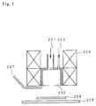
- ECR-PECVD device electronic cyclotron resonance plasma CVD device used in the Example is schematically shown in FIG.1.
- the oxygen plasma was formed by guiding 2.45 GHz microwaves to a reaction chamber 202 through a waveguide 201 and feeding 100 SCCM of oxygen from the gas-feed pipe 203
- the reaction chamber interior pressure was 1.84 mtorr and the output of the microwaves was 2500 W.
- An outside coil 204 was provided around the outside of the reaction chamber for applying a magnetic field of 875 Gauss to the oxygen plasma so that the electrons in the plasma satisfied the ECR condition.
- the substrate 205 was placed perpendicular to the plasma, and the substrate temperature was kept 300 °C by the heater 206.
- the oxygen plasma 807 was radiated for 8 minutes 20 seconds to oxidize that of the amorphous silicon thin film 808 left at the position for the channel region to be formed in, and an SiO 2 film 808 which was to be a part of a gate insulating film was formed. Below the part which was to be a part of the gate insulating layer that of the amorphous silicon thin film 809 which was to be the channel region was left. (FIG. 2E).
- an SiO 2 film 810 which was to be the gate insulating layer was deposited.
- This SiO 2 film 810 was deposited using 60 SCCM of silane and 100 SCCM of oxygen at a 2250 microwave output, a 300 °C substrate temperature and for 18.7 seconds.
- the reaction chamber pressure was 2.62 mtorr.
- the thus-formed multi-layer films were measured by a multi-wavelength dispersive ellipsometry (multi-wavelength spectroellipsometry, MOSS-ES 4G, by Soaplar).
- the remaining amorphous silicon film 809 which was to be formed in the channel portion had 205 ⁇ .
- the SiO 2 film formed by the oxidation of the amorphous silicon film 808 had 120 ⁇ .
- the SiO 2 film 810 had 1500 ⁇ . At the wavelength of 632.8 nm the refractive indices of the SiO 2 film 808 and the SiO 2 film 810 were 1.42 and 1.40 respectively.
- the thus-prepared substrate was inserted in a 600 °C-electric furnace and was heat-treated for 48 hours.
- the electric furnace was kept supplied with 99.999 % or higher purity nitrogen gas at 20 I/min. to maintain an inert ambient atmosphere.
- This heat-treatment at 600 °C in the inert ambient atmosphere crystallized the amorphous silicon left on the part which was to be the channel region to be transformed into a silicon thin film 811 constituting the channel region (FIG. 2E).
- this substrate was placed again into the ECR-PECVD to radiate a hydrogen plasma to the heat-treated substrate.
- the hydrogen plasma was formed using 100 SCCM of hydrogen at a 300 °C substrate temperature and a 2000 W microwave output. In this state, the reaction chamber interior pressure was 1.97 mtorr, and the hydrogen plasma radiation was conducted for 45 minutes.
- chrome was deposited in 1500 ⁇ by sputtering.
- a gate electrode 812 was formed by patterning. At this time the sheet resistance was 1.36 ⁇ /square.
- a contact hole was formed in the gate insulating film, and a source and a drain electrode 813 were formed by sputtering or other techniques, and a transistor was completed by patterning (FIG. 2F).
- the material of the source and the drain electrodes aluminum of a 8000 ⁇ -thickness was used. The sheet resistance of this aluminum was 42 m ⁇ /square.
- TFT thin film transistor
- Ids (ordinate) denotes a source-drain current.
- Ids 34.5 ⁇ A.
- the resultant thin film semiconductor device had such good transistor characteristic.
- the field effect mobility of this transistor based on the saturation current region was 12.52 cm 2 /V ⁇ sec.
- the transistor characteristic of a thin film semiconductor device fabricated by the prior art is shown as a control at 9-b.
- This thin film semiconductor device fabricated by the prior art was fabricated by the same process as the Example except that the channel silicon thin film of the former was deposited at 600 °C by low pressure CVD, and the oxygen plasma was not radiated.
- the device for depositing the channel silicon thin film by low pressure CVD was the same as that used in the Example in depositing the amorphous silicon thin film.
- the channel silicon thin film was deposited in 1 252 ⁇ -thickness using 24 SCCM of monosilane as the raw material gas at a reaction furnace interior pressure of 13.8 mtorr and a 19.00 ⁇ /min. depositing speed.
- a thin film semiconductor device was fabricated by the same process as the Example except that the channel silicon thin film which was deposited at 600 °C by low pressure CVD as done in the above-described prior art was subjected to oxygen plasma radiation before the deposition of the gate insulating film.
- the TFT characteristic of this thin film semiconductor device was measured. The TFT characteristic did not substantially change due to the oxygen plasma radiation, and the Vgs-lds curve of this TFT, which was subjected to the oxygen plasma radiation agreed with that of 9-b.
- the oxygen plasma radiation is not much effective in the prior art in which the channel silicon thin film is deposited at 600 °C by low pressure CVD.
- the TFT characteristic of a thin film semiconductor device fabricated by further another prior art is shown at 9-c.
- This thin film semiconductor device was fabricated by the same process as the Example except that the oxygen plasma radiation was not conducted. That is, an amorphous silicon thin film was deposited as the channel silicon layer and then was subjected to heat-treatment at 600 °C. But the oxygen plasma radiation was not conducted before the formation of the gate insulating layer.
- the TFT fabricated by this prior art had a depletion of -10 V and had a poor rise characteristic.
- the field effect mobility was 9.94 cm 2 /V ⁇ sec.
- the transistor characteristic of the thin film semiconductor device is drastically improved only when the amorphous silicon thin film which is to be the channel region is radiated with an oxygen plasma and then heat-treated to crystallize the channel silicon thin film. This is because the oxidation of the surface of the amorphous silicon film by the oxygen plasma produces clean MIS interfaces, and the crystallization is performed.
- the example of this invention has much better semiconductor characteristics than those fabricated by the prior art.
Landscapes
- Thin Film Transistor (AREA)
- Recrystallisation Techniques (AREA)
Claims (2)
- Procédé de fabrication d'un dispositif semi-conducteur à couches minces par un traitement à basse température, dont les étapes sont exécutées à une température maximum égale ou inférieure à environ 600°C, comprenant :une première étape consistant à former une couche de silicium amorphe sur une surface isolante d'un substrat,une deuxième étape consistant à supprimer des couches d'oxyde naturel en immergeant le substrat dans une solution de nettoyage aqueuse contenant de l'acide fluorhydrique,une troisième étape consistant à irradier un plasma d'oxygène sur la couche de silicium amorphe pour former une première couche isolante de grille,une quatrième étape consistant à former une deuxième couche isolante de grille par le procédé de dépôt chimique en phase vapeur sur la première couche isolante de grille consécutivement à la troisième étape,une cinquième étape consistant à traiter par la chaleur le substrat ainsi préparé à 600°C sous une atmosphère ambiante inerte de façon à faire cristalliser la couche de silicium amorphe, etune sixième étape consistant à former une électrode de grille sur la deuxième couche isolante, les première à sixième étapes étant exécutées dans cet ordre.
- Procédé selon la revendication 1, dans lequel ladite première étape sert à former une couche de silicium pour une zone de canal d'un transistor à couches minces.
Applications Claiming Priority (9)
| Application Number | Priority Date | Filing Date | Title |
|---|---|---|---|
| JP31047790 | 1990-11-16 | ||
| JP310477/90 | 1990-11-16 | ||
| JP31047790 | 1990-11-16 | ||
| JP7640691 | 1991-04-09 | ||
| JP7640691 | 1991-04-09 | ||
| JP76406/91 | 1991-04-09 | ||
| JP23509891 | 1991-09-13 | ||
| JP235098/91 | 1991-09-13 | ||
| JP23509891 | 1991-09-13 |
Publications (3)
| Publication Number | Publication Date |
|---|---|
| EP0486047A2 EP0486047A2 (fr) | 1992-05-20 |
| EP0486047A3 EP0486047A3 (en) | 1996-04-10 |
| EP0486047B1 true EP0486047B1 (fr) | 1999-09-01 |
Family
ID=27302149
Family Applications (1)
| Application Number | Title | Priority Date | Filing Date |
|---|---|---|---|
| EP91119529A Expired - Lifetime EP0486047B1 (fr) | 1990-11-16 | 1991-11-15 | Procédé de fabrication d'un dispositif semi-conducteur en couche mince |
Country Status (5)
| Country | Link |
|---|---|
| US (5) | US5372958A (fr) |
| EP (1) | EP0486047B1 (fr) |
| KR (1) | KR100283350B1 (fr) |
| DE (1) | DE69131570T2 (fr) |
| SG (1) | SG63578A1 (fr) |
Cited By (1)
| Publication number | Priority date | Publication date | Assignee | Title |
|---|---|---|---|---|
| US8067297B2 (en) | 2001-02-12 | 2011-11-29 | Asm America, Inc. | Process for deposition of semiconductor films |
Families Citing this family (126)
| Publication number | Priority date | Publication date | Assignee | Title |
|---|---|---|---|---|
| EP0486047B1 (fr) * | 1990-11-16 | 1999-09-01 | Seiko Epson Corporation | Procédé de fabrication d'un dispositif semi-conducteur en couche mince |
| US7115902B1 (en) | 1990-11-20 | 2006-10-03 | Semiconductor Energy Laboratory Co., Ltd. | Electro-optical device and method for manufacturing the same |
| KR950013784B1 (ko) * | 1990-11-20 | 1995-11-16 | 가부시키가이샤 한도오따이 에네루기 겐큐쇼 | 반도체 전계효과 트랜지스터 및 그 제조방법과 박막트랜지스터 |
| US5849601A (en) | 1990-12-25 | 1998-12-15 | Semiconductor Energy Laboratory Co., Ltd. | Electro-optical device and method for manufacturing the same |
| US7576360B2 (en) | 1990-12-25 | 2009-08-18 | Semiconductor Energy Laboratory Co., Ltd. | Electro-optical device which comprises thin film transistors and method for manufacturing the same |
| US7098479B1 (en) | 1990-12-25 | 2006-08-29 | Semiconductor Energy Laboratory Co., Ltd. | Electro-optical device and method for manufacturing the same |
| EP0499979A3 (en) | 1991-02-16 | 1993-06-09 | Semiconductor Energy Laboratory Co., Ltd. | Electro-optical device |
| JP2794678B2 (ja) * | 1991-08-26 | 1998-09-10 | 株式会社 半導体エネルギー研究所 | 絶縁ゲイト型半導体装置およびその作製方法 |
| JP2717237B2 (ja) | 1991-05-16 | 1998-02-18 | 株式会社 半導体エネルギー研究所 | 絶縁ゲイト型半導体装置およびその作製方法 |
| JPH05249478A (ja) * | 1991-12-25 | 1993-09-28 | Toshiba Corp | 液晶表示装置 |
| US5576222A (en) * | 1992-01-27 | 1996-11-19 | Tdk Corp. | Method of making a semiconductor image sensor device |
| KR950005484B1 (ko) * | 1992-09-29 | 1995-05-24 | 현대전자산업주식회사 | 플라즈마 산화 처리를 이용한 폴리실리콘 박막트랜지스터 제조방법 |
| KR100250020B1 (ko) * | 1993-03-02 | 2000-03-15 | 가네꼬 히사시 | 반도체 소자용 다결정 실리콘 박막 형성 방법(method of forming polycrystalline silicon thin films for semiconductor devices) |
| FR2702882B1 (fr) * | 1993-03-16 | 1995-07-28 | Thomson Lcd | Procédé de fabrication de transistors à couches minces étagés directs. |
| US6730549B1 (en) | 1993-06-25 | 2004-05-04 | Semiconductor Energy Laboratory Co., Ltd. | Semiconductor device and method for its preparation |
| JP2677167B2 (ja) * | 1993-07-08 | 1997-11-17 | 日本電気株式会社 | 駆動回路内蔵型液晶表示装置の製造方法 |
| US5663077A (en) | 1993-07-27 | 1997-09-02 | Semiconductor Energy Laboratory Co., Ltd. | Method of manufacturing a thin film transistor in which the gate insulator comprises two oxide films |
| JPH0766424A (ja) * | 1993-08-20 | 1995-03-10 | Semiconductor Energy Lab Co Ltd | 半導体装置およびその作製方法 |
| TW297142B (fr) | 1993-09-20 | 1997-02-01 | Handotai Energy Kenkyusho Kk | |
| US6897100B2 (en) | 1993-11-05 | 2005-05-24 | Semiconductor Energy Laboratory Co., Ltd. | Method for processing semiconductor device apparatus for processing a semiconductor and apparatus for processing semiconductor device |
| CN100367461C (zh) | 1993-11-05 | 2008-02-06 | 株式会社半导体能源研究所 | 一种制造薄膜晶体管和电子器件的方法 |
| JP2646977B2 (ja) * | 1993-11-29 | 1997-08-27 | 日本電気株式会社 | 順スタガ型薄膜トランジスタの製造方法 |
| US7081938B1 (en) | 1993-12-03 | 2006-07-25 | Semiconductor Energy Laboratory Co., Ltd. | Electro-optical device and method for manufacturing the same |
| JP3254072B2 (ja) * | 1994-02-15 | 2002-02-04 | 株式会社半導体エネルギー研究所 | 半導体装置の作製方法 |
| US5620906A (en) | 1994-02-28 | 1997-04-15 | Semiconductor Energy Laboratory Co., Ltd. | Method for producing semiconductor device by introducing hydrogen ions |
| FR2719416B1 (fr) * | 1994-04-29 | 1996-07-05 | Thomson Lcd | Procédé de passivation des flancs d'un composant semiconducteur à couches minces. |
| KR100327086B1 (ko) * | 1994-06-15 | 2002-03-06 | 구사마 사부로 | 박막 반도체 장치의 제조방법, 박막 반도체 장치,액정표시장치 및 전자기기 |
| US6706572B1 (en) | 1994-08-31 | 2004-03-16 | Semiconductor Energy Laboratory Co., Ltd. | Method for manufacturing a thin film transistor using a high pressure oxidation step |
| KR0147019B1 (ko) * | 1994-12-21 | 1998-09-15 | 김광호 | 박막트랜지스터 액정 디스플레이 소자의 패드부 및 박막트랜지스터 액정디스플레이 소자의 제조방법 |
| US5726720A (en) * | 1995-03-06 | 1998-03-10 | Canon Kabushiki Kaisha | Liquid crystal display apparatus in which an insulating layer between the source and substrate is thicker than the insulating layer between the drain and substrate |
| US6372534B1 (en) | 1995-06-06 | 2002-04-16 | Lg. Philips Lcd Co., Ltd | Method of making a TFT array with photo-imageable insulating layer over address lines |
| US6228751B1 (en) * | 1995-09-08 | 2001-05-08 | Semiconductor Energy Laboratory Co., Ltd. | Method of manufacturing a semiconductor device |
| JP3645379B2 (ja) * | 1996-01-19 | 2005-05-11 | 株式会社半導体エネルギー研究所 | 半導体装置の作製方法 |
| JP3645378B2 (ja) | 1996-01-19 | 2005-05-11 | 株式会社半導体エネルギー研究所 | 半導体装置の作製方法 |
| US6478263B1 (en) * | 1997-01-17 | 2002-11-12 | Semiconductor Energy Laboratory Co., Ltd. | Semiconductor device and its manufacturing method |
| JP3729955B2 (ja) | 1996-01-19 | 2005-12-21 | 株式会社半導体エネルギー研究所 | 半導体装置の作製方法 |
| JP3645380B2 (ja) | 1996-01-19 | 2005-05-11 | 株式会社半導体エネルギー研究所 | 半導体装置の作製方法、情報端末、ヘッドマウントディスプレイ、ナビゲーションシステム、携帯電話、ビデオカメラ、投射型表示装置 |
| US5985740A (en) | 1996-01-19 | 1999-11-16 | Semiconductor Energy Laboratory Co., Ltd. | Method of manufacturing a semiconductor device including reduction of a catalyst |
| US5888858A (en) | 1996-01-20 | 1999-03-30 | Semiconductor Energy Laboratory Co., Ltd. | Semiconductor device and fabrication method thereof |
| US7056381B1 (en) * | 1996-01-26 | 2006-06-06 | Semiconductor Energy Laboratory Co., Ltd. | Fabrication method of semiconductor device |
| US6180439B1 (en) * | 1996-01-26 | 2001-01-30 | Semiconductor Energy Laboratory Co., Ltd. | Method for fabricating a semiconductor device |
| US6465287B1 (en) | 1996-01-27 | 2002-10-15 | Semiconductor Energy Laboratory Co., Ltd. | Method for fabricating a semiconductor device using a metal catalyst and high temperature crystallization |
| US6121163A (en) | 1996-02-09 | 2000-09-19 | Applied Materials, Inc. | Method and apparatus for improving the film quality of plasma enhanced CVD films at the interface |
| KR100192593B1 (ko) * | 1996-02-21 | 1999-07-01 | 윤종용 | 폴리 실리콘 박막 트랜지스터의 제조방법 |
| US6100562A (en) | 1996-03-17 | 2000-08-08 | Semiconductor Energy Laboratory Co., Ltd. | Method of manufacturing a semiconductor device |
| US6013583A (en) * | 1996-06-25 | 2000-01-11 | International Business Machines Corporation | Low temperature BPSG deposition process |
| FR2751131B1 (fr) * | 1996-07-09 | 2001-11-09 | Lg Electronics Inc | Procede de fabrication d'un dispositif d'affichage a matrice active a cristal liquide et structure du dispositif d'affichage selon ce procede |
| US6188452B1 (en) | 1996-07-09 | 2001-02-13 | Lg Electronics, Inc | Active matrix liquid crystal display and method of manufacturing same |
| US5658808A (en) * | 1996-08-14 | 1997-08-19 | Industrial Technology Research Institute | Method of fabricating polycrystalline silicon thin-film transistor having symmetrical lateral resistors |
| US5759618A (en) * | 1997-02-27 | 1998-06-02 | Diamond Seal, Inc. | Glass coating cmposition and method of application |
| US6083272A (en) * | 1997-06-13 | 2000-07-04 | Advanced Micro Devices, Inc. | Method of adjusting currents on a semiconductor device having transistors of varying density |
| US5989963A (en) * | 1997-07-21 | 1999-11-23 | Advanced Micro Devices, Inc. | Method for obtaining a steep retrograde channel profile |
| GB9726511D0 (en) * | 1997-12-13 | 1998-02-11 | Philips Electronics Nv | Thin film transistors and electronic devices comprising such |
| JP3713380B2 (ja) * | 1998-03-04 | 2005-11-09 | 株式会社東芝 | 薄膜の形成方法および装置 |
| JP4223092B2 (ja) * | 1998-05-19 | 2009-02-12 | 株式会社半導体エネルギー研究所 | 半導体装置の作製方法 |
| JP2000058839A (ja) * | 1998-08-05 | 2000-02-25 | Semiconductor Energy Lab Co Ltd | 半導体素子からなる半導体回路を備えた半導体装置およびその作製方法 |
| US6662631B2 (en) * | 1998-08-28 | 2003-12-16 | Interuniversitair Microelektronica Centrum | Method and apparatus for characterization of porous films |
| US6077750A (en) * | 1998-10-27 | 2000-06-20 | Lg Semicon Co., Ltd. | Method for forming epitaxial Co self-align silicide for semiconductor device |
| US6180476B1 (en) * | 1998-11-06 | 2001-01-30 | Advanced Micro Devices, Inc. | Dual amorphization implant process for ultra-shallow drain and source extensions |
| US6297115B1 (en) | 1998-11-06 | 2001-10-02 | Advanced Micro Devices, Inc. | Cmos processs with low thermal budget |
| US6225173B1 (en) | 1998-11-06 | 2001-05-01 | Advanced Micro Devices, Inc. | Recessed channel structure for manufacturing shallow source/drain extensions |
| US6200869B1 (en) | 1998-11-06 | 2001-03-13 | Advanced Micro Devices, Inc. | Method of fabricating an integrated circuit with ultra-shallow source/drain extensions |
| US6265291B1 (en) | 1999-01-04 | 2001-07-24 | Advanced Micro Devices, Inc. | Circuit fabrication method which optimizes source/drain contact resistance |
| US6245649B1 (en) | 1999-02-17 | 2001-06-12 | Advanced Micro Devices, Inc. | Method for forming a retrograde impurity profile |
| US6197669B1 (en) | 1999-04-15 | 2001-03-06 | Taiwan Semicondcutor Manufacturing Company | Reduction of surface defects on amorphous silicon grown by a low-temperature, high pressure LPCVD process |
| US6194748B1 (en) | 1999-05-03 | 2001-02-27 | Advanced Micro Devices, Inc. | MOSFET with suppressed gate-edge fringing field effect |
| US6492249B2 (en) | 1999-05-03 | 2002-12-10 | Advanced Micro Devices, Inc. | High-K gate dielectric process with process with self aligned damascene contact to damascene gate and a low-k inter level dielectric |
| US6291278B1 (en) | 1999-05-03 | 2001-09-18 | Advanced Micro Devices, Inc. | Method of forming transistors with self aligned damascene gate contact |
| US6271132B1 (en) | 1999-05-03 | 2001-08-07 | Advanced Micro Devices, Inc. | Self-aligned source and drain extensions fabricated in a damascene contact and gate process |
| US6265293B1 (en) | 1999-08-27 | 2001-07-24 | Advanced Micro Devices, Inc. | CMOS transistors fabricated in optimized RTA scheme |
| US6403433B1 (en) | 1999-09-16 | 2002-06-11 | Advanced Micro Devices, Inc. | Source/drain doping technique for ultra-thin-body SOI MOS transistors |
| US6465315B1 (en) | 2000-01-03 | 2002-10-15 | Advanced Micro Devices, Inc. | MOS transistor with local channel compensation implant |
| US7019363B1 (en) | 2000-01-04 | 2006-03-28 | Advanced Micro Devices, Inc. | MOS transistor with asymmetrical source/drain extensions |
| TW449928B (en) | 2000-01-25 | 2001-08-11 | Samsung Electronics Co Ltd | A low temperature polycrystalline silicon type thin film transistor and a method of the thin film transistor fabrication |
| US6333244B1 (en) | 2000-01-26 | 2001-12-25 | Advanced Micro Devices, Inc. | CMOS fabrication process with differential rapid thermal anneal scheme |
| US6372589B1 (en) | 2000-04-19 | 2002-04-16 | Advanced Micro Devices, Inc. | Method of forming ultra-shallow source/drain extension by impurity diffusion from doped dielectric spacer |
| US6420218B1 (en) | 2000-04-24 | 2002-07-16 | Advanced Micro Devices, Inc. | Ultra-thin-body SOI MOS transistors having recessed source and drain regions |
| US6746901B2 (en) * | 2000-05-12 | 2004-06-08 | Semiconductor Energy Laboratory Co., Ltd. | Semiconductor device and method of fabricating thereof |
| US6368947B1 (en) | 2000-06-20 | 2002-04-09 | Advanced Micro Devices, Inc. | Process utilizing a cap layer optimized to reduce gate line over-melt |
| US6361874B1 (en) | 2000-06-20 | 2002-03-26 | Advanced Micro Devices, Inc. | Dual amorphization process optimized to reduce gate line over-melt |
| US6399450B1 (en) | 2000-07-05 | 2002-06-04 | Advanced Micro Devices, Inc. | Low thermal budget process for manufacturing MOS transistors having elevated source and drain regions |
| US6630386B1 (en) | 2000-07-18 | 2003-10-07 | Advanced Micro Devices, Inc | CMOS manufacturing process with self-amorphized source/drain junctions and extensions |
| US6521502B1 (en) | 2000-08-07 | 2003-02-18 | Advanced Micro Devices, Inc. | Solid phase epitaxy activation process for source/drain junction extensions and halo regions |
| US6472282B1 (en) | 2000-08-15 | 2002-10-29 | Advanced Micro Devices, Inc. | Self-amorphized regions for transistors |
| US6756277B1 (en) | 2001-02-09 | 2004-06-29 | Advanced Micro Devices, Inc. | Replacement gate process for transistors having elevated source and drain regions |
| US6403434B1 (en) | 2001-02-09 | 2002-06-11 | Advanced Micro Devices, Inc. | Process for manufacturing MOS transistors having elevated source and drain regions and a high-k gate dielectric |
| US6495437B1 (en) | 2001-02-09 | 2002-12-17 | Advanced Micro Devices, Inc. | Low temperature process to locally form high-k gate dielectrics |
| US6787424B1 (en) | 2001-02-09 | 2004-09-07 | Advanced Micro Devices, Inc. | Fully depleted SOI transistor with elevated source and drain |
| US6551885B1 (en) | 2001-02-09 | 2003-04-22 | Advanced Micro Devices, Inc. | Low temperature process for a thin film transistor |
| US7026219B2 (en) | 2001-02-12 | 2006-04-11 | Asm America, Inc. | Integration of high k gate dielectric |
| JP3901460B2 (ja) * | 2001-02-19 | 2007-04-04 | 株式会社日立製作所 | 薄膜トランジスタの製造方法 |
| US6420776B1 (en) | 2001-03-01 | 2002-07-16 | Amkor Technology, Inc. | Structure including electronic components singulated using laser cutting |
| US6830994B2 (en) * | 2001-03-09 | 2004-12-14 | Semiconductor Energy Laboratory Co., Ltd. | Method of manufacturing a semiconductor device having a crystallized semiconductor film |
| US6833313B2 (en) * | 2001-04-13 | 2004-12-21 | Semiconductor Energy Laboratory Co., Ltd. | Method of manufacturing semiconductor device by implanting rare gas ions |
| US7294582B2 (en) | 2002-07-19 | 2007-11-13 | Asm International, N.V. | Low temperature silicon compound deposition |
| US7297641B2 (en) | 2002-07-19 | 2007-11-20 | Asm America, Inc. | Method to form ultra high quality silicon-containing compound layers |
| US7186630B2 (en) | 2002-08-14 | 2007-03-06 | Asm America, Inc. | Deposition of amorphous silicon-containing films |
| KR20040021758A (ko) * | 2002-09-04 | 2004-03-11 | 엘지.필립스 엘시디 주식회사 | 다결정 실리콘 박막트랜지스터 제조방법 |
| JP4627964B2 (ja) * | 2002-10-24 | 2011-02-09 | 株式会社半導体エネルギー研究所 | 半導体装置の作製方法 |
| JP4004448B2 (ja) * | 2003-09-24 | 2007-11-07 | 富士通株式会社 | 半導体装置およびその製造方法 |
| US7312125B1 (en) | 2004-02-05 | 2007-12-25 | Advanced Micro Devices, Inc. | Fully depleted strained semiconductor on insulator transistor and method of making the same |
| US7629270B2 (en) | 2004-08-27 | 2009-12-08 | Asm America, Inc. | Remote plasma activated nitridation |
| US7966969B2 (en) | 2004-09-22 | 2011-06-28 | Asm International N.V. | Deposition of TiN films in a batch reactor |
| US7629267B2 (en) | 2005-03-07 | 2009-12-08 | Asm International N.V. | High stress nitride film and method for formation thereof |
| US20060275975A1 (en) * | 2005-06-01 | 2006-12-07 | Matt Yeh | Nitridated gate dielectric layer |
| US10690847B2 (en) * | 2005-06-15 | 2020-06-23 | Braggone Oy | Method of making a photonic crystal device and photonic crystal device |
| US7657143B2 (en) * | 2005-10-07 | 2010-02-02 | Novatronix Corporation | Method for improving refractive index control in PECVD deposited a-SiNy films |
| US7718518B2 (en) | 2005-12-16 | 2010-05-18 | Asm International N.V. | Low temperature doped silicon layer formation |
| US7691757B2 (en) | 2006-06-22 | 2010-04-06 | Asm International N.V. | Deposition of complex nitride films |
| KR20080070327A (ko) * | 2007-01-26 | 2008-07-30 | 삼성전자주식회사 | 박막 트랜지스터, 이를 포함하는 유기 발광 표시 장치 및그 제조 방법 |
| US7629256B2 (en) | 2007-05-14 | 2009-12-08 | Asm International N.V. | In situ silicon and titanium nitride deposition |
| US20090227061A1 (en) * | 2008-03-05 | 2009-09-10 | Nicholas Bateman | Establishing a high phosphorus concentration in solar cells |
| US20090224250A1 (en) * | 2008-03-10 | 2009-09-10 | Hidayat Kisdarjono | Top Gate Thin Film Transistor with Enhanced Off Current Suppression |
| US8896065B2 (en) * | 2008-04-14 | 2014-11-25 | Sharp Laboratories Of America, Inc. | Top gate thin film transistor with independent field control for off-current suppression |
| US7833906B2 (en) | 2008-12-11 | 2010-11-16 | Asm International N.V. | Titanium silicon nitride deposition |
| JP5711146B2 (ja) | 2008-12-24 | 2015-04-30 | スリーエム イノベイティブ プロパティズ カンパニー | 金属酸化物半導体薄膜トランジスタにおける安定性の向上 |
| US8912080B2 (en) | 2011-01-12 | 2014-12-16 | Semiconductor Energy Laboratory Co., Ltd. | Manufacturing method of the semiconductor device |
| WO2013039126A1 (fr) | 2011-09-16 | 2013-03-21 | Semiconductor Energy Laboratory Co., Ltd. | Dispositif à semiconducteur |
| US9082663B2 (en) | 2011-09-16 | 2015-07-14 | Semiconductor Energy Laboratory Co., Ltd. | Semiconductor device and manufacturing method thereof |
| US8952379B2 (en) | 2011-09-16 | 2015-02-10 | Semiconductor Energy Laboratory Co., Ltd. | Semiconductor device |
| US9653614B2 (en) | 2012-01-23 | 2017-05-16 | Semiconductor Energy Laboratory Co., Ltd. | Semiconductor device and method for manufacturing the same |
| JP5788355B2 (ja) * | 2012-03-29 | 2015-09-30 | 東京エレクトロン株式会社 | 熱処理システム、熱処理方法、及び、プログラム |
| KR20130136063A (ko) * | 2012-06-04 | 2013-12-12 | 삼성디스플레이 주식회사 | 박막 트랜지스터, 이를 포함하는 박막 트랜지스터 표시판 및 그 제조 방법 |
| TWI518430B (zh) * | 2013-12-02 | 2016-01-21 | 群創光電股份有限公司 | 顯示面板及應用其之顯示裝置 |
| CN103730384A (zh) * | 2013-12-13 | 2014-04-16 | 深圳市华星光电技术有限公司 | 一种tft电性量测方法及装置 |
| CN103852951B (zh) * | 2014-02-19 | 2016-11-16 | 南京大学 | 利用纳米硅和二氧化硅界面态来提高非线性光学性能的方法 |
Citations (3)
| Publication number | Priority date | Publication date | Assignee | Title |
|---|---|---|---|---|
| US4156619A (en) * | 1975-06-11 | 1979-05-29 | Wacker-Chemitronic Gesellschaft Fur Elektronik-Grundstoffe Mbh | Process for cleaning semi-conductor discs |
| EP0154670A2 (fr) * | 1978-06-14 | 1985-09-18 | Fujitsu Limited | Procédé pour la fabrication d'un dispositif semi-conducteur comportant une couche isolante |
| US4882649A (en) * | 1988-03-29 | 1989-11-21 | Texas Instruments Incorporated | Nitride/oxide/nitride capacitor dielectric |
Family Cites Families (50)
| Publication number | Priority date | Publication date | Assignee | Title |
|---|---|---|---|---|
| JPS5685869A (en) * | 1979-12-17 | 1981-07-13 | Nec Corp | Manufacture of semiconductor device |
| FR2527385B1 (fr) * | 1982-04-13 | 1987-05-22 | Suwa Seikosha Kk | Transistor a couche mince et panneau d'affichage a cristaux liquides utilisant ce type de transistor |
| US4411734A (en) * | 1982-12-09 | 1983-10-25 | Rca Corporation | Etching of tantalum silicide/doped polysilicon structures |
| JPH0682839B2 (ja) * | 1984-08-21 | 1994-10-19 | セイコー電子工業株式会社 | 表示用パネルの製造方法 |
| JPH0680826B2 (ja) * | 1985-08-20 | 1994-10-12 | 富士通株式会社 | 薄膜トランジスタの製造方法 |
| US4804640A (en) * | 1985-08-27 | 1989-02-14 | General Electric Company | Method of forming silicon and aluminum containing dielectric film and semiconductor device including said film |
| US4675978A (en) * | 1985-09-09 | 1987-06-30 | Rca Corporation | Method for fabricating a radiation hardened oxide having two portions |
| US4634473A (en) * | 1985-09-09 | 1987-01-06 | Rca Corporation | Method for fabricating a radiation hardened oxide having structural damage |
| JPS6266629A (ja) * | 1985-09-19 | 1987-03-26 | Fujitsu Ltd | 薄膜形成方法 |
| JPS6292329A (ja) * | 1985-10-17 | 1987-04-27 | Sharp Corp | 絶縁膜形成方法 |
| JPS631071A (ja) * | 1986-06-20 | 1988-01-06 | Hitachi Ltd | 薄膜半導体装置 |
| JPS6331110A (ja) * | 1986-07-25 | 1988-02-09 | Fujitsu Ltd | 半導体装置の製造方法 |
| JPS6358875A (ja) * | 1986-08-29 | 1988-03-14 | Hitachi Ltd | 薄膜トランジスタ素子 |
| US4859908A (en) * | 1986-09-24 | 1989-08-22 | Matsushita Electric Industrial Co., Ltd. | Plasma processing apparatus for large area ion irradiation |
| KR900007686B1 (ko) * | 1986-10-08 | 1990-10-18 | 후지쓰 가부시끼가이샤 | 선택적으로 산화된 실리콘 기판상에 에피택셜 실리콘층과 다결정 실리콘층을 동시에 성장시키는 기상 증착방법 |
| JP2503001B2 (ja) * | 1987-02-19 | 1996-06-05 | 富士通株式会社 | 薄膜トランジスタの製造方法 |
| JPS63232337A (ja) * | 1987-03-20 | 1988-09-28 | Hitachi Ltd | ドライクリ−ニング方法 |
| JPS63273323A (ja) * | 1987-05-01 | 1988-11-10 | Nippon Telegr & Teleph Corp <Ntt> | 膜形成装置 |
| JPS63316479A (ja) * | 1987-06-19 | 1988-12-23 | Hitachi Ltd | 薄膜トランジスタおよびその製造方法 |
| JPS6435958A (en) * | 1987-07-30 | 1989-02-07 | Ricoh Kk | Thin film transistor |
| JPS6484229A (en) * | 1987-09-28 | 1989-03-29 | Nippon Soken | Thin film transistor |
| JP2589327B2 (ja) * | 1987-11-14 | 1997-03-12 | 株式会社リコー | 薄膜トランジスタの製造方法 |
| JP2677808B2 (ja) * | 1987-12-12 | 1997-11-17 | 工業技術院長 | 電界効果型トランジスタ |
| JPH0228322A (ja) * | 1988-04-28 | 1990-01-30 | Mitsubishi Electric Corp | 半導体基板の前処理方法 |
| NL8801379A (nl) * | 1988-05-30 | 1989-12-18 | Imec Inter Uni Micro Electr | Werkwijze voor het vervaardigen van een dunne-filmtransistor en een dergelijke dunne-filmtransistor. |
| GB8813349D0 (en) * | 1988-06-06 | 1988-07-13 | Gen Electric Co Plc | Amplifiers |
| JPH0246776A (ja) * | 1988-08-09 | 1990-02-16 | Toshiba Corp | 半導体装置 |
| JPH0282577A (ja) * | 1988-09-19 | 1990-03-23 | Seiko Epson Corp | 薄膜トランジスタの製造方法 |
| JP2841381B2 (ja) * | 1988-09-19 | 1998-12-24 | セイコーエプソン株式会社 | 薄膜トランジスタの製造方法 |
| JP3055782B2 (ja) * | 1988-09-19 | 2000-06-26 | セイコーエプソン株式会社 | 薄膜トランジスタの製造方 |
| CA1313563C (fr) * | 1988-10-26 | 1993-02-09 | Makoto Sasaki | Panneau de transistors en couches minces |
| US4997746A (en) * | 1988-11-22 | 1991-03-05 | Greco Nancy A | Method of forming conductive lines and studs |
| EP0608503B1 (fr) * | 1989-02-14 | 1997-05-28 | Seiko Epson Corporation | Dispositif semi-conducteur et son procédé de fabrication |
| US5231297A (en) * | 1989-07-14 | 1993-07-27 | Sanyo Electric Co., Ltd. | Thin film transistor |
| JPH03104209A (ja) * | 1989-09-19 | 1991-05-01 | Seiko Epson Corp | 半導体装置の製造方法 |
| US5190792A (en) * | 1989-09-27 | 1993-03-02 | International Business Machines Corporation | High-throughput, low-temperature process for depositing oxides |
| GB2238683A (en) * | 1989-11-29 | 1991-06-05 | Philips Electronic Associated | A thin film transistor circuit |
| JP2602336B2 (ja) * | 1989-11-29 | 1997-04-23 | 株式会社日立製作所 | プラズマ処理装置 |
| US5231296A (en) * | 1989-12-19 | 1993-07-27 | Texas Instruments Incorporated | Thin film transistor structure with insulating mask |
| JPH0637317A (ja) * | 1990-04-11 | 1994-02-10 | General Motors Corp <Gm> | 薄膜トランジスタおよびその製造方法 |
| JP2796175B2 (ja) * | 1990-06-05 | 1998-09-10 | 松下電器産業株式会社 | 薄膜トランジスターの製造方法 |
| US5147826A (en) * | 1990-08-06 | 1992-09-15 | The Pennsylvania Research Corporation | Low temperature crystallization and pattering of amorphous silicon films |
| JPH04102375A (ja) * | 1990-08-22 | 1992-04-03 | Ricoh Co Ltd | 薄膜トランジスタ |
| KR920005267A (ko) * | 1990-08-24 | 1992-03-28 | 야마무라 가쓰미 | 반도체장치의 제조방법 |
| US5064775A (en) * | 1990-09-04 | 1991-11-12 | Industrial Technology Research Institute | Method of fabricating an improved polycrystalline silicon thin film transistor |
| EP0486047B1 (fr) * | 1990-11-16 | 1999-09-01 | Seiko Epson Corporation | Procédé de fabrication d'un dispositif semi-conducteur en couche mince |
| JP2508948B2 (ja) * | 1991-06-21 | 1996-06-19 | 日本電気株式会社 | 半導体装置の製造方法 |
| EP0553791A1 (fr) * | 1992-01-31 | 1993-08-04 | Nec Corporation | Electrode de condensateur pour DRAM et procédé de sa manufacture |
| JPH05250244A (ja) * | 1992-03-04 | 1993-09-28 | Nec Corp | データベースシステム |
| KR0161887B1 (ko) * | 1995-12-26 | 1999-02-18 | 문정환 | 용기를 갖는 습식에치 장치의 에치 종말점 측정방법 |
-
1991
- 1991-11-15 EP EP91119529A patent/EP0486047B1/fr not_active Expired - Lifetime
- 1991-11-15 DE DE69131570T patent/DE69131570T2/de not_active Expired - Lifetime
- 1991-11-15 SG SG1996003651A patent/SG63578A1/en unknown
- 1991-11-15 US US07/792,436 patent/US5372958A/en not_active Expired - Lifetime
-
1994
- 1994-07-07 US US08/271,861 patent/US5504019A/en not_active Expired - Lifetime
- 1994-08-17 US US08/291,764 patent/US5591989A/en not_active Expired - Lifetime
-
1995
- 1995-05-02 US US08/434,338 patent/US5637512A/en not_active Expired - Lifetime
-
1996
- 1996-09-27 US US08/724,235 patent/US5811323A/en not_active Expired - Lifetime
-
2000
- 2000-02-02 KR KR1020000005116A patent/KR100283350B1/ko not_active Expired - Lifetime
Patent Citations (3)
| Publication number | Priority date | Publication date | Assignee | Title |
|---|---|---|---|---|
| US4156619A (en) * | 1975-06-11 | 1979-05-29 | Wacker-Chemitronic Gesellschaft Fur Elektronik-Grundstoffe Mbh | Process for cleaning semi-conductor discs |
| EP0154670A2 (fr) * | 1978-06-14 | 1985-09-18 | Fujitsu Limited | Procédé pour la fabrication d'un dispositif semi-conducteur comportant une couche isolante |
| US4882649A (en) * | 1988-03-29 | 1989-11-21 | Texas Instruments Incorporated | Nitride/oxide/nitride capacitor dielectric |
Non-Patent Citations (3)
| Title |
|---|
| Halbleitertechnologie, W. Harth, Teubner Studienskripten 1981, p. 49 * |
| Motorola/Technical Developments 8 (1988), no. 1, p. 3, 4 * |
| VLSI Technology, S.M. Sze ed., McGraw-Hill 1983, p. 463 * |
Cited By (2)
| Publication number | Priority date | Publication date | Assignee | Title |
|---|---|---|---|---|
| US8067297B2 (en) | 2001-02-12 | 2011-11-29 | Asm America, Inc. | Process for deposition of semiconductor films |
| US8360001B2 (en) | 2001-02-12 | 2013-01-29 | Asm America, Inc. | Process for deposition of semiconductor films |
Also Published As
| Publication number | Publication date |
|---|---|
| US5504019A (en) | 1996-04-02 |
| KR100283350B1 (ko) | 2001-02-15 |
| US5591989A (en) | 1997-01-07 |
| EP0486047A2 (fr) | 1992-05-20 |
| DE69131570D1 (de) | 1999-10-07 |
| DE69131570T2 (de) | 2000-02-17 |
| EP0486047A3 (en) | 1996-04-10 |
| SG63578A1 (en) | 1999-03-30 |
| US5372958A (en) | 1994-12-13 |
| US5637512A (en) | 1997-06-10 |
| US5811323A (en) | 1998-09-22 |
Similar Documents
| Publication | Publication Date | Title |
|---|---|---|
| US5811323A (en) | Process for fabricating a thin film transistor | |
| US5275851A (en) | Low temperature crystallization and patterning of amorphous silicon films on electrically insulating substrates | |
| US5879973A (en) | Method for fabricating thin-film transistor | |
| KR100191091B1 (ko) | 박막 반도체 장치와 그 제조방법 | |
| US5328861A (en) | Method for forming thin film transistor | |
| US6500736B2 (en) | Crystallization method of amorphous silicon | |
| US6570184B2 (en) | Thin film transistor and method for manufacturing the same | |
| JPH06267849A (ja) | 半導体素子の作製方法 | |
| KR20030060403A (ko) | 비정질 실리콘의 결정화 방법 | |
| US6531348B2 (en) | Method for crystallizing amorphous silicon and fabricating thin film transistor using crystallized silicon | |
| US7026200B2 (en) | Method for manufacturing a semiconductor device | |
| KR20020057382A (ko) | 반도체 소자 제조 방법 및 장치 | |
| US7435667B2 (en) | Method of controlling polysilicon crystallization | |
| US5733793A (en) | Process formation of a thin film transistor | |
| US20020149017A1 (en) | Active matrix display device having high intensity and high precision and manufacturing method thereof | |
| JP3486421B2 (ja) | 薄膜半導体装置の製造方法 | |
| KR100205069B1 (ko) | 다결정 실리콘 박막 트랜지스터의 제조방법 | |
| EP0073603B1 (fr) | Transistor à film mince polycristallin et circuit intégré comprenant un tel transistor et dispositif d'affichage comprenant un tel circuit | |
| JP3510973B2 (ja) | 薄膜半導体装置の製造方法 | |
| JP2759411B2 (ja) | 半導体装置およびその作製方法 | |
| JP2002299235A (ja) | 半導体薄膜形成方法及び薄膜半導体装置 | |
| JP3038898B2 (ja) | 薄膜半導体装置の製造方法 | |
| JPH10223911A (ja) | 薄膜半導体装置 | |
| JPH06181178A (ja) | 薄膜トランジスタの製造方法 | |
| KR19990023052A (ko) | 비정질 막을 결정화하는 방법 |
Legal Events
| Date | Code | Title | Description |
|---|---|---|---|
| PUAI | Public reference made under article 153(3) epc to a published international application that has entered the european phase |
Free format text: ORIGINAL CODE: 0009012 |
|
| AK | Designated contracting states |
Kind code of ref document: A2 Designated state(s): DE FR GB NL |
|
| PUAL | Search report despatched |
Free format text: ORIGINAL CODE: 0009013 |
|
| AK | Designated contracting states |
Kind code of ref document: A3 Designated state(s): DE FR GB NL |
|
| 17P | Request for examination filed |
Effective date: 19960329 |
|
| 17Q | First examination report despatched |
Effective date: 19960821 |
|
| GRAG | Despatch of communication of intention to grant |
Free format text: ORIGINAL CODE: EPIDOS AGRA |
|
| GRAG | Despatch of communication of intention to grant |
Free format text: ORIGINAL CODE: EPIDOS AGRA |
|
| GRAH | Despatch of communication of intention to grant a patent |
Free format text: ORIGINAL CODE: EPIDOS IGRA |
|
| RBV | Designated contracting states (corrected) |
Designated state(s): DE |
|
| GRAH | Despatch of communication of intention to grant a patent |
Free format text: ORIGINAL CODE: EPIDOS IGRA |
|
| GRAA | (expected) grant |
Free format text: ORIGINAL CODE: 0009210 |
|
| AK | Designated contracting states |
Kind code of ref document: B1 Designated state(s): DE |
|
| REF | Corresponds to: |
Ref document number: 69131570 Country of ref document: DE Date of ref document: 19991007 |
|
| PLBE | No opposition filed within time limit |
Free format text: ORIGINAL CODE: 0009261 |
|
| STAA | Information on the status of an ep patent application or granted ep patent |
Free format text: STATUS: NO OPPOSITION FILED WITHIN TIME LIMIT |
|
| 26N | No opposition filed | ||
| PGFP | Annual fee paid to national office [announced via postgrant information from national office to epo] |
Ref country code: DE Payment date: 20101110 Year of fee payment: 20 |
|
| REG | Reference to a national code |
Ref country code: DE Ref legal event code: R071 Ref document number: 69131570 Country of ref document: DE |
|
| REG | Reference to a national code |
Ref country code: DE Ref legal event code: R071 Ref document number: 69131570 Country of ref document: DE |
|
| PG25 | Lapsed in a contracting state [announced via postgrant information from national office to epo] |
Ref country code: DE Free format text: LAPSE BECAUSE OF EXPIRATION OF PROTECTION Effective date: 20111116 |