EP0492991A2 - Verfahren zum Gettern und zur Kontrolle der Ausbildung von Defekten während der Herstellung von doppelt-diffundierten integrierten Schaltkreiszellen und so hergestellte Zelle - Google Patents
Verfahren zum Gettern und zur Kontrolle der Ausbildung von Defekten während der Herstellung von doppelt-diffundierten integrierten Schaltkreiszellen und so hergestellte Zelle Download PDFInfo
- Publication number
- EP0492991A2 EP0492991A2 EP91311810A EP91311810A EP0492991A2 EP 0492991 A2 EP0492991 A2 EP 0492991A2 EP 91311810 A EP91311810 A EP 91311810A EP 91311810 A EP91311810 A EP 91311810A EP 0492991 A2 EP0492991 A2 EP 0492991A2
- Authority
- EP
- European Patent Office
- Prior art keywords
- silicon
- conductivity type
- region
- range
- gettering
- Prior art date
- Legal status (The legal status is an assumption and is not a legal conclusion. Google has not performed a legal analysis and makes no representation as to the accuracy of the status listed.)
- Granted
Links
Images





Classifications
-
- H—ELECTRICITY
- H10—SEMICONDUCTOR DEVICES; ELECTRIC SOLID-STATE DEVICES NOT OTHERWISE PROVIDED FOR
- H10D—INORGANIC ELECTRIC SEMICONDUCTOR DEVICES
- H10D30/00—Field-effect transistors [FET]
- H10D30/60—Insulated-gate field-effect transistors [IGFET]
- H10D30/64—Double-diffused metal-oxide semiconductor [DMOS] FETs
- H10D30/66—Vertical DMOS [VDMOS] FETs
-
- H—ELECTRICITY
- H10—SEMICONDUCTOR DEVICES; ELECTRIC SOLID-STATE DEVICES NOT OTHERWISE PROVIDED FOR
- H10D—INORGANIC ELECTRIC SEMICONDUCTOR DEVICES
- H10D30/00—Field-effect transistors [FET]
- H10D30/01—Manufacture or treatment
- H10D30/021—Manufacture or treatment of FETs having insulated gates [IGFET]
- H10D30/028—Manufacture or treatment of FETs having insulated gates [IGFET] of double-diffused metal oxide semiconductor [DMOS] FETs
- H10D30/0291—Manufacture or treatment of FETs having insulated gates [IGFET] of double-diffused metal oxide semiconductor [DMOS] FETs of vertical DMOS [VDMOS] FETs
-
- H—ELECTRICITY
- H10—SEMICONDUCTOR DEVICES; ELECTRIC SOLID-STATE DEVICES NOT OTHERWISE PROVIDED FOR
- H10D—INORGANIC ELECTRIC SEMICONDUCTOR DEVICES
- H10D30/00—Field-effect transistors [FET]
- H10D30/60—Insulated-gate field-effect transistors [IGFET]
- H10D30/64—Double-diffused metal-oxide semiconductor [DMOS] FETs
- H10D30/66—Vertical DMOS [VDMOS] FETs
- H10D30/665—Vertical DMOS [VDMOS] FETs having edge termination structures
-
- H—ELECTRICITY
- H10—SEMICONDUCTOR DEVICES; ELECTRIC SOLID-STATE DEVICES NOT OTHERWISE PROVIDED FOR
- H10D—INORGANIC ELECTRIC SEMICONDUCTOR DEVICES
- H10D62/00—Semiconductor bodies, or regions thereof, of devices having potential barriers
- H10D62/10—Shapes, relative sizes or dispositions of the regions of the semiconductor bodies; Shapes of the semiconductor bodies
- H10D62/124—Shapes, relative sizes or dispositions of the regions of semiconductor bodies or of junctions between the regions
- H10D62/126—Top-view geometrical layouts of the regions or the junctions
- H10D62/127—Top-view geometrical layouts of the regions or the junctions of cellular field-effect devices, e.g. multicellular DMOS transistors or IGBTs
-
- H—ELECTRICITY
- H10—SEMICONDUCTOR DEVICES; ELECTRIC SOLID-STATE DEVICES NOT OTHERWISE PROVIDED FOR
- H10D—INORGANIC ELECTRIC SEMICONDUCTOR DEVICES
- H10D62/00—Semiconductor bodies, or regions thereof, of devices having potential barriers
- H10D62/10—Shapes, relative sizes or dispositions of the regions of the semiconductor bodies; Shapes of the semiconductor bodies
- H10D62/17—Semiconductor regions connected to electrodes not carrying current to be rectified, amplified or switched, e.g. channel regions
- H10D62/393—Body regions of DMOS transistors or IGBTs
-
- H—ELECTRICITY
- H10—SEMICONDUCTOR DEVICES; ELECTRIC SOLID-STATE DEVICES NOT OTHERWISE PROVIDED FOR
- H10D—INORGANIC ELECTRIC SEMICONDUCTOR DEVICES
- H10D64/00—Electrodes of devices having potential barriers
- H10D64/01—Manufacture or treatment
- H10D64/013—Manufacture or treatment of electrodes having a conductor capacitively coupled to a semiconductor by an insulator
- H10D64/01302—Manufacture or treatment of electrodes having a conductor capacitively coupled to a semiconductor by an insulator the insulator being formed after the semiconductor body, the semiconductor being silicon
- H10D64/01332—Making the insulator
- H10D64/01336—Making the insulator on single crystalline silicon, e.g. chemical oxidation using a liquid
- H10D64/01344—Making the insulator on single crystalline silicon, e.g. chemical oxidation using a liquid in a nitrogen-containing ambient, e.g. N2O oxidation
-
- H—ELECTRICITY
- H10—SEMICONDUCTOR DEVICES; ELECTRIC SOLID-STATE DEVICES NOT OTHERWISE PROVIDED FOR
- H10D—INORGANIC ELECTRIC SEMICONDUCTOR DEVICES
- H10D64/00—Electrodes of devices having potential barriers
- H10D64/01—Manufacture or treatment
- H10D64/013—Manufacture or treatment of electrodes having a conductor capacitively coupled to a semiconductor by an insulator
- H10D64/01302—Manufacture or treatment of electrodes having a conductor capacitively coupled to a semiconductor by an insulator the insulator being formed after the semiconductor body, the semiconductor being silicon
- H10D64/01332—Making the insulator
- H10D64/01336—Making the insulator on single crystalline silicon, e.g. chemical oxidation using a liquid
- H10D64/01346—Making the insulator on single crystalline silicon, e.g. chemical oxidation using a liquid in a gaseous ambient using an oxygen or a water vapour, e.g. oxidation through a layer
-
- H—ELECTRICITY
- H10—SEMICONDUCTOR DEVICES; ELECTRIC SOLID-STATE DEVICES NOT OTHERWISE PROVIDED FOR
- H10D—INORGANIC ELECTRIC SEMICONDUCTOR DEVICES
- H10D64/00—Electrodes of devices having potential barriers
- H10D64/60—Electrodes characterised by their materials
- H10D64/66—Electrodes having a conductor capacitively coupled to a semiconductor by an insulator, e.g. MIS electrodes
- H10D64/68—Electrodes having a conductor capacitively coupled to a semiconductor by an insulator, e.g. MIS electrodes characterised by the insulator, e.g. by the gate insulator
- H10D64/681—Electrodes having a conductor capacitively coupled to a semiconductor by an insulator, e.g. MIS electrodes characterised by the insulator, e.g. by the gate insulator having a compositional variation, e.g. multilayered
- H10D64/685—Electrodes having a conductor capacitively coupled to a semiconductor by an insulator, e.g. MIS electrodes characterised by the insulator, e.g. by the gate insulator having a compositional variation, e.g. multilayered being perpendicular to the channel plane
-
- H—ELECTRICITY
- H10—SEMICONDUCTOR DEVICES; ELECTRIC SOLID-STATE DEVICES NOT OTHERWISE PROVIDED FOR
- H10D—INORGANIC ELECTRIC SEMICONDUCTOR DEVICES
- H10D64/00—Electrodes of devices having potential barriers
- H10D64/60—Electrodes characterised by their materials
- H10D64/66—Electrodes having a conductor capacitively coupled to a semiconductor by an insulator, e.g. MIS electrodes
- H10D64/68—Electrodes having a conductor capacitively coupled to a semiconductor by an insulator, e.g. MIS electrodes characterised by the insulator, e.g. by the gate insulator
- H10D64/693—Electrodes having a conductor capacitively coupled to a semiconductor by an insulator, e.g. MIS electrodes characterised by the insulator, e.g. by the gate insulator the insulator comprising nitrogen, e.g. nitrides, oxynitrides or nitrogen-doped materials
-
- H—ELECTRICITY
- H10—SEMICONDUCTOR DEVICES; ELECTRIC SOLID-STATE DEVICES NOT OTHERWISE PROVIDED FOR
- H10P—GENERIC PROCESSES OR APPARATUS FOR THE MANUFACTURE OR TREATMENT OF DEVICES COVERED BY CLASS H10
- H10P14/00—Formation of materials, e.g. in the shape of layers or pillars
- H10P14/60—Formation of materials, e.g. in the shape of layers or pillars of insulating materials
- H10P14/63—Formation of materials, e.g. in the shape of layers or pillars of insulating materials characterised by the formation processes
- H10P14/6302—Non-deposition formation processes
- H10P14/6304—Formation by oxidation, e.g. oxidation of the substrate
- H10P14/6306—Formation by oxidation, e.g. oxidation of the substrate of the semiconductor materials
- H10P14/6308—Formation by oxidation, e.g. oxidation of the substrate of the semiconductor materials of Group IV semiconductors
- H10P14/6309—Formation by oxidation, e.g. oxidation of the substrate of the semiconductor materials of Group IV semiconductors of silicon in uncombined form, i.e. pure silicon
-
- H—ELECTRICITY
- H10—SEMICONDUCTOR DEVICES; ELECTRIC SOLID-STATE DEVICES NOT OTHERWISE PROVIDED FOR
- H10P—GENERIC PROCESSES OR APPARATUS FOR THE MANUFACTURE OR TREATMENT OF DEVICES COVERED BY CLASS H10
- H10P14/00—Formation of materials, e.g. in the shape of layers or pillars
- H10P14/60—Formation of materials, e.g. in the shape of layers or pillars of insulating materials
- H10P14/63—Formation of materials, e.g. in the shape of layers or pillars of insulating materials characterised by the formation processes
- H10P14/6302—Non-deposition formation processes
- H10P14/6322—Formation by thermal treatments
-
- H—ELECTRICITY
- H10—SEMICONDUCTOR DEVICES; ELECTRIC SOLID-STATE DEVICES NOT OTHERWISE PROVIDED FOR
- H10P—GENERIC PROCESSES OR APPARATUS FOR THE MANUFACTURE OR TREATMENT OF DEVICES COVERED BY CLASS H10
- H10P14/00—Formation of materials, e.g. in the shape of layers or pillars
- H10P14/60—Formation of materials, e.g. in the shape of layers or pillars of insulating materials
- H10P14/65—Formation of materials, e.g. in the shape of layers or pillars of insulating materials characterised by treatments performed before or after the formation of the materials
- H10P14/6502—Formation of materials, e.g. in the shape of layers or pillars of insulating materials characterised by treatments performed before or after the formation of the materials of treatments performed before formation of the materials
- H10P14/6512—Formation of materials, e.g. in the shape of layers or pillars of insulating materials characterised by treatments performed before or after the formation of the materials of treatments performed before formation of the materials by exposure to a gas or vapour
-
- H—ELECTRICITY
- H10—SEMICONDUCTOR DEVICES; ELECTRIC SOLID-STATE DEVICES NOT OTHERWISE PROVIDED FOR
- H10P—GENERIC PROCESSES OR APPARATUS FOR THE MANUFACTURE OR TREATMENT OF DEVICES COVERED BY CLASS H10
- H10P36/00—Gettering within semiconductor bodies
- H10P36/03—Gettering within semiconductor bodies within silicon bodies
Definitions
- the present invention relates to integrated circuits and to the fabrication of such circuits, with particular reference to the fabrication of low defect DMOSFET structures.
- SMP60N05 Siliconix Incorporated, Santa Clara, California.
- This device is an N-channel enhancement mode transistor packaged in a TO-220AB case.
- the technology used to fabricate the SMP60N05 product is characterized by a specific on-resistance of 3.5 micro-ohms/cm2.
- junction depths range from 2.5 to 5 microns for the body, from 5 to 6 microns for the p+ body contact, and from 0.5 to 1 micron for the n+ source regions.
- the cell configuration is square.
- the present invention facilitates the realization of a reduced r DS(on) and a higher MOSFET cell density, which promotes more efficient load management switching and allows the use of smaller or no heat sinks.
- the present invention facilitates the realization of a lower gate charge for the same specified on-resistance of earlier devices, which allows the use of small drive circuits and fewer components.
- a method for initially oxidizing a silicon body with steam for forming a power MOS device is performed with 1 - 6 percent TCA at 1000 - 1250 degrees C.
- gettering is performed with 0.5 - 5 percent TCA at a temperature in the range of 900 - 1100 degrees C.
- gettering is performed with 0.5 - 5 percent TCA at a temperature in the range of 900 - 1200 degrees C.
- a heavily doped p+ region of less than 2.5 micron junction depth is formed for a power MOS device with the steps of boron injection, boron soak, and low temperature oxidation in the range of 800 - 1200 degrees C.
- each corner of a double diffusion defining perimeter is greater than 120 degrees.
- a method for forming a silicon power MOS device on a silicon body comprises the steps of forming a first mask overlaying the silicon body; opening a window though the first mask into a diffusion site in the silicon body; diffusing a first dopant into the diffusion site through the window; removing the first mask from the silicon body; providing an oxide layer of less than about 1000 Angstroms in thickness over the diffusion site and proximate regions of the silicon body; and providing a second mask thicker than the first mask over at least a portion of the diffusion site; and diffusing a second dopant.
- a termination structure for a power device comprises a silicon body; a gate oxide overlaying the silicon body; and a polysilicon layer overlaying the gate oxide in a scribe region of the power device.
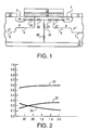
- a cross-sectional structure of an n-channel power MOSFET with its simplified resistive equivalent circuit is illustrated in Figure 1.
- a n-type lightly doped epitaxial silicon layer 1 includes various diffused regions such as the deep p+ regions 2 and 3, p body regions 4 and 5, and n+ source regions 6 and 7.
- a typically continuous source-body electrode 12 extends across certain surface portions of the epitaxial layer 1.
- a drain electrode 14 is provided at the backside of the n+ doped substrate (not separately shown).
- An insulated gate structure comprising gate oxide 16 and polysilicon 18 is provided over the drain and portions of the body, the latter functioning as MOSFET channel regions.
- the principal elements of the simplified resistive circuit include the channel resistances 20 and 21, the JFET resistance 22, 23 and 24, and the epi resistance 26.
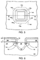
- Figure 2 is a graph showing the on-resistance contribution of the channel regions 20 and 21, the JFET region 22, 23 and 24, and the epi region 26 for an arbitrary 60 volt n-channel DMOSFET.
- V GS is 10 volts
- temperature is 25 degrees C
- each square cell measures 10 microns by 10 microns
- the cell space is 6 microns.
- Curve 30 represents the ratio of the channel resistance 20 to R DS
- curve 32 represents the ratio of the JFET resistance 24 to R DS
- curve 34 represents the ratio of the epi resistance 26 to R DS .
- on-resistance is dominated by the channel resistance 20 and 21, the JFET resistance 24 is generally of secondary significance, and the epi resistance 26 is generally of tertiary significance.
- a typical square cell such as used in the previously mentioned product number SMP60N05 is shown in Figures 3 and 4, prior to metallization.
- the edge of the polysilicon gate 40, which overlays gate oxide 42, is used in the double diffusion process to define the channel 44.
- the channel lies within p body region 50, between source region 52 and drain region 54 in the epitaxial layer 46.
- the channel length for the square cells of any given device is in the range of from about 1.5 microns to about 4 microns, reflecting the comparatively deep drive-in used to form the variously doped epitaxial regions described above.
- the polysilicon gate 40 is covered with a layer of oxide 56.
- the first diffusion of the double diffusion process which is described in detail below, is a rather lightly p-type diffusion which is strongly driven in to a depth of from 2.5 microns to 5 microns.
- p-type dopant diffuses horizontally at a rate of about 80 percent of vertical diffusion. Due to the spreading effect in the corners, the effective rate of horizontal diffusion is much less, on the order of merely 50 percent.
- Punch-through is a condition in which the depletion region reaches into the n+ source, thereby causing conductance through the reverse-biased device and leading to device breakdown. Punch-through would occur because the three dimensional diffusion effect would cause the channel 44 to be excessively short at the corners 48a, 48b 48c and 48d.
- the diffusions are kept shallow and the length of channel 144 brought into the range of from 0.5 to 0.75 microns, for example.
- Typical junction depths in this event would be about 2.5 - 3 microns for the p-tub 160, about 2 - 2.5 microns for the p+ body contact 158, about 1 - 1.25 microns for the p body 150, and about 0.3 - 0.6 microns for the n+ source region 152.
- a heavily doped shallow region such as p+ body contact 158 would lower the breakdown voltage by up to 40 percent compared to earlier devices built on the same epi specifications (doping and thickness). This difficulty is overcome in accordance with the present invention by providing the lightly doped p- tub 160, which forms a linearly graded pn junction, resulting in improved breakdown voltage.
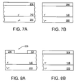
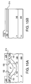
- Figures 7-17 The process for forming the cell of Figures 5 and 6 is illustrated in Figures 7-17. Part A of Figures 7-17 are cross-sectional views taken through a typical cell, while part B of Figures 7-17 are cross-sectional views taken through the termination region at the periphery of the chip.
- Suitable starting material includes a n+ doped silicon substrate 200 having a resistivity in the range of, for example, from 0.001 to 0.005 ohm-cm, supporting a n- doped epitaxial layer 146 having a resistivity of, for example, from 0.15 to 1 ohm-cm.
- a thermally grown field oxide 204 is grown by any suitable process such as, for example, a thermal process to a thickness in the range of for example, 5000 to 10,000 Angstroms, as shown in Figure 7.
- the first masking step is for the diffusion of the p- tub and the p+ body contact.
- a window 206 is opened in the field oxide 204 over the cell region by any suitable process such as, for example, a dry oxide etch.
- the resist is suitably stripped, and the p- tub implant is made ( Figure 9) with Boron at a dose in the range of 1E13 - 1E14 /cm2, at a power in the range of 40 - 100 KeV.
- the Boron implant is diffused at a temperature of from 1000 to 1250 degrees C for from 2-10 hours using any suitable oven to form the p- tub 160.
- a wet etch in a suitable HF solution is carried out to remove any resulting oxide, and the p+ body contact is formed by injecting Boron from a boron nitride source in any suitable furnace through the window 206 at 750 - 1000 degrees C.
- a Boron rich glass 212 forms in the window 206 during the injection.
- a Boron soak is carried out in any suitable oven at 750 - 1000 degrees C for from 15 minutes to 3 hours, as appropriate, wherein boron from the glass continues to diffuse into the epitaxial silicon to form p+ body contact 158 in the p- tub 160 ( Figure 10).
- the sheet resistance of the p+ body contact is 10 - 100 ohm/square.
- the field oxide 204 is protected in the peripheral termination region, including gate finger regions. All oxide is removed from the active device areas, and gate oxide 214 is thermally grown at 900 -1100 degrees C for from 20 minutes to 3 hours, as desired ( Figure 11).
- a polysilicon film is deposited to a thickness of 0.3 -0.7 microns using any suitable equipment.
- a polysilicon film also is deposited on the backside, and is removed along with an underlying oxide in a wet oxide etch for the purpose of exposing the wafer backside to heavy diffusion using phosphorus or other suitable dopant.
- the polysilicon film is then doped to less than about 20 ohm/square, and is patterned in a third masking step for opening windows to form p- body, n+ source regions, and ultimately metal contacts to the source and body.
- the polysilicon film is etched in any suitable equipment, to form gate poly 216 and periphery strip 218, a component of a termination structure.
- the resist is stripped, and Boron is implanted at a dose of 5E13 - 2E14 /cm2 and a power of 40 - 100 KeV in any suitable equipment ( Figure 13).
- the Boron is diffused at 900 - 1200 degrees C for 10 minutes to 5 hours, as desired.
- the purpose of this diffusion is to form the double diffused channel 144.
- Oxide is etched from the p- body diffusion region using either a dry or wet etch, as desired, and a layer of suitable photoresist is deposited and patterned in a fourth masking step to form a body contact mask (Figure 14).
- An Arsenic implant is made using a dose of 1E15 - 1E16 /cm2 at a power of 60 - 120KeV, after which the resist is stripped ( Figure 15) and the Arsenic diffused at 850 - 1100 degrees C for 0.5 - 1 hour to form the square source region 152.
- An oxide layer 220 forms during the Arsenic diffusion (Figure 16).
- the square channel 144 is defined in the body 158, between the square source region 152 and the drain 154. At this point, the junction profile of the cell is essentially established.
- the device is completed by depositing (optionally) about 1000 Angstroms of LPCVD nitride 222 followed by a BPSG deposition of about 0.8 - 1.3 microns and a BPSG reflow 224 at about 850 - 1000 degrees C (Figure 16).
- the fifth masking step is a contact mask, which defines the source-body contact and the poly gate contact.
- the BPSG layer 224, the nitride layer 222, and the oxide layer 220 are suitably etched in a sequence involving, for example, a descum, a dry etch in suitable equipment, and a resist strip, followed by a reflow of the BPSG at 850 - 1100 degrees C for 10 - 30 minutes ( Figure 17).
- a suitable metal such as aluminum or a material such as aluminum with 1 percent silicon is deposited using, for example, sputter deposition, and is suitably patterned in a sixth masking step and etched to form the source electrode 226, the gate electrode (not shown), and termination field plates (not shown). Films of PSG 228 and/or plasma nitride 230 are deposited, pad contact holes are opened in a seventh masking step, and an alloy step is performed at 300 - 450 degrees C in an inert ambient.
- the termination structure 234 comprising field oxide 204, gate oxide 214, and polysilicon periphery strip 218 need only be coupled electrostaticly to the epitaxial silicon 146 in order to function satisfactorily. The coupling is achieved when the die is separated from the wafer by dicing, since the thin gate oxide 214 near the die edge is damaged and becomes leaky.
- the termination structure 234 assumes the voltage level of the epitaxial layer 146, and at this potential acts to exclude the depletion region from the leaky damaged silicon at the die edge.
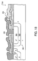
- Figure 18 shows the full termination structure, including a typical inactive cell 300.
- the inactive cell 300 is similar to the active cells except no channel region is provided, although a p- tub 302 and p+ body contact 304 are provided.
- Source metal 306 shorts a polysilicon ring 308 and the inactive cell 300 to the source electrode. Note the termination structure 234.
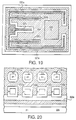
- Figure 19 shows a plan view of a completed device with the gate fingers 320a-320e, gate bonding pad 322, source metal 324, and source bonding pad 326.
- the exploded view of Figure 20 shows the juxtaposition of the active cells 330a-330d (other active cells in the device are not shown), the inactive cells 332a-332d (other inactive cells in the device are not shown), the gate finger 320e, and the p+ polysilicon ring 334.
- TCA or trichloroethane is incorporated in the process gases for most of the temperature treatment to control silicon defect forementioned.
- the percentage of TCA in the ambient has to be optimized, and too much TCA will result in silicon pitting due to HCl etching and the carbon-induced defects.
- For each temperature treatment begin at 750 degrees C and ramp up to final temperature, which under some circumstances is 1250 degrees C.
- TCA gettering at high temperature provides intrinsic gettering and furnace cleaning for oxide quality improvement and stacking fault reduction.
- TCA in the range of 1 - 6 percent at a temperature in the range of 1000 - 1250 degrees C is suitable.
- TCA gettering at high temperature anneals implant defects in silicon and reduces stacking fault formation.
- the three step Boron process for the p+ body contact which involves Boron injection, Boron soak, and low temperature oxidation in the range discussed above avoids fatal defects and achieves a low sheet resistance as discussed above.
- TCA gettering with minimizing carbon contamination achieves oxide rupture voltage enhancement and minimize defect formation.
- a suitable TCA concentration is in the range of 0.5 - 5 percent at a temperature in the range of 900 - 1100 degrees C is required to optimize the process since too much TCA will induce carbon-related defects, as explained above.
- TCA gettering with high temperature anneal implantation damage achieves silicon defect reduction.
- a suitable TCA concentration is 0.5 - 5 percent at a temperature in the range of 900 - 1200 degrees C to gain optimized process that will satisfy the shallow junction requirements and without suffering defect loss.
- a high temperature anneal before reoxidation in TCA/02 ambient achieves silicon defect reduction.
- a suitable TCA concentration is 0.5 - 5 percent at a temperature in the range of 850 - 1100 degrees C.
- the silicon is slightly etched to eliminate auto doping from the BPSG during reflow. This minimizes the contact resistance variation.
Landscapes
- Insulated Gate Type Field-Effect Transistor (AREA)
- Metal-Oxide And Bipolar Metal-Oxide Semiconductor Integrated Circuits (AREA)
- Electrodes Of Semiconductors (AREA)
- Thin Film Transistor (AREA)
Priority Applications (1)
| Application Number | Priority Date | Filing Date | Title |
|---|---|---|---|
| EP98203152A EP0890994A3 (de) | 1990-12-21 | 1991-12-19 | Leistungs-MOSFET und Herstellungsverfahren |
Applications Claiming Priority (4)
| Application Number | Priority Date | Filing Date | Title |
|---|---|---|---|
| US63157390A | 1990-12-21 | 1990-12-21 | |
| US63156990A | 1990-12-21 | 1990-12-21 | |
| US631573 | 1990-12-21 | ||
| US631569 | 1990-12-21 |
Related Child Applications (1)
| Application Number | Title | Priority Date | Filing Date |
|---|---|---|---|
| EP98203152A Division EP0890994A3 (de) | 1990-12-21 | 1991-12-19 | Leistungs-MOSFET und Herstellungsverfahren |
Publications (3)
| Publication Number | Publication Date |
|---|---|
| EP0492991A2 true EP0492991A2 (de) | 1992-07-01 |
| EP0492991A3 EP0492991A3 (en) | 1993-01-07 |
| EP0492991B1 EP0492991B1 (de) | 1999-06-23 |
Family
ID=27091427
Family Applications (2)
| Application Number | Title | Priority Date | Filing Date |
|---|---|---|---|
| EP91311810A Expired - Lifetime EP0492991B1 (de) | 1990-12-21 | 1991-12-19 | Verfahren zur Herstellung von doppelt-diffundierten integrierten MOSFET-Zellen |
| EP98203152A Withdrawn EP0890994A3 (de) | 1990-12-21 | 1991-12-19 | Leistungs-MOSFET und Herstellungsverfahren |
Family Applications After (1)
| Application Number | Title | Priority Date | Filing Date |
|---|---|---|---|
| EP98203152A Withdrawn EP0890994A3 (de) | 1990-12-21 | 1991-12-19 | Leistungs-MOSFET und Herstellungsverfahren |
Country Status (3)
| Country | Link |
|---|---|
| EP (2) | EP0492991B1 (de) |
| JP (3) | JP2807114B2 (de) |
| DE (1) | DE69131376T2 (de) |
Cited By (9)
| Publication number | Priority date | Publication date | Assignee | Title |
|---|---|---|---|---|
| EP0598438A1 (de) * | 1992-11-17 | 1994-05-25 | Koninklijke Philips Electronics N.V. | Verfahren zur Diffundierung von einem Dotierstoff in einem Halbleiter |
| US5496742A (en) * | 1993-02-22 | 1996-03-05 | Nec Corporation | Method for manufacturing semiconductor device enabling gettering effect |
| WO1998035384A1 (de) * | 1997-02-06 | 1998-08-13 | Siemens Aktiengesellschaft | Oxidschicht für einen liegenden halbleiterkörper |
| CN1099713C (zh) * | 1995-04-06 | 2003-01-22 | 工业技术研究院 | 用n边多边形单元布线的mos单元、多单元晶体管及ic芯片 |
| EP0635888B1 (de) * | 1993-07-22 | 2006-03-01 | Siliconix Incorporated | Struktur und Herstellung von Leistungs-MOSFET unter Einbeziehung der Struktur des Randes |
| EP1753022A1 (de) * | 2005-08-12 | 2007-02-14 | STMicroelectronics S.r.l. | Halbleiter-Leistungsbauelement mit Mehrfach-Drain-Struktur und entsprechendes Herstellungsverfahren |
| US8207784B2 (en) | 2008-02-12 | 2012-06-26 | Semi Solutions, Llc | Method and apparatus for MOSFET drain-source leakage reduction |
| CN112701151A (zh) * | 2019-10-23 | 2021-04-23 | 株洲中车时代电气股份有限公司 | SiC MOSFET器件的制造方法及SiC MOSFET器件 |
| US12660299B2 (en) | 2022-05-17 | 2026-06-16 | Vishay Siliconix Llc | MOSFET device |
Families Citing this family (7)
| Publication number | Priority date | Publication date | Assignee | Title |
|---|---|---|---|---|
| JP2006165406A (ja) * | 2004-12-10 | 2006-06-22 | Renesas Technology Corp | 半導体装置およびその製造方法 |
| JP4963364B2 (ja) * | 2006-03-02 | 2012-06-27 | 日本インター株式会社 | 半導体装置の製造方法 |
| KR100877266B1 (ko) * | 2007-05-18 | 2009-01-09 | 주식회사 동부하이텍 | 엘디모스 채널 형성방법 |
| CN105244279B (zh) * | 2014-07-10 | 2018-09-25 | 北大方正集团有限公司 | 一种平面型vdmos器件及其制作方法 |
| JP6481511B2 (ja) * | 2014-07-24 | 2019-03-13 | 住友電気工業株式会社 | 炭化珪素半導体装置 |
| CN105470297B (zh) * | 2014-09-10 | 2018-09-28 | 北大方正集团有限公司 | 一种vdmos器件及其制作方法 |
| CN105845576A (zh) * | 2015-01-16 | 2016-08-10 | 北大方正集团有限公司 | 超结mosfet的制作方法 |
Family Cites Families (24)
| Publication number | Priority date | Publication date | Assignee | Title |
|---|---|---|---|---|
| DE2603747A1 (de) * | 1976-01-31 | 1977-08-04 | Licentia Gmbh | Integrierte schaltungsanordnung |
| DE3012430A1 (de) * | 1980-03-31 | 1981-10-08 | Siemens AG, 1000 Berlin und 8000 München | Planare halbleiteranordnung mit erhoehter durchbruchsspannung |
| JPS57106040A (en) * | 1980-12-22 | 1982-07-01 | Sony Corp | Prevention of stacking fault |
| JPS57107072A (en) * | 1980-12-25 | 1982-07-03 | Fujitsu Ltd | Manufacture of semiconductor device |
| DE3220250A1 (de) * | 1982-05-28 | 1983-12-01 | Siemens AG, 1000 Berlin und 8000 München | Halbleiterbauelement mit planarstruktur |
| JPS5914676A (ja) * | 1982-07-16 | 1984-01-25 | Nec Corp | 縦型電界効果トランジスタの製造方法 |
| JPS5987871A (ja) * | 1982-11-12 | 1984-05-21 | Hitachi Ltd | 絶縁ゲ−ト電界効果半導体装置 |
| US4803532A (en) * | 1982-11-27 | 1989-02-07 | Nissan Motor Co., Ltd. | Vertical MOSFET having a proof structure against puncture due to breakdown |
| GB2134705B (en) * | 1983-01-28 | 1985-12-24 | Philips Electronic Associated | Semiconductor devices |
| JPS6010677A (ja) * | 1983-06-30 | 1985-01-19 | Nissan Motor Co Ltd | 縦型mosトランジスタ |
| DE3326383A1 (de) * | 1983-07-22 | 1985-01-31 | Siemens AG, 1000 Berlin und 8000 München | Schottkydiode |
| JPS60160168A (ja) * | 1984-01-30 | 1985-08-21 | Toshiba Corp | Mos型半導体装置の製造方法 |
| JPS60196974A (ja) * | 1984-03-19 | 1985-10-05 | Toshiba Corp | 導電変調型mosfet |
| US4620211A (en) * | 1984-08-13 | 1986-10-28 | General Electric Company | Method of reducing the current gain of an inherent bipolar transistor in an insulated-gate semiconductor device and resulting devices |
| JPS61274366A (ja) * | 1985-05-29 | 1986-12-04 | Tdk Corp | 高耐圧半導体装置 |
| EP0279403A3 (de) * | 1987-02-16 | 1988-12-07 | Nec Corporation | Vertikaler MOS-Feldeffekttransistor mit hoher Spannungsfestigkeit und hoher Schaltgeschwindigkeit |
| JPH01272163A (ja) * | 1987-08-07 | 1989-10-31 | Fuji Electric Co Ltd | 半導体装置の製造方法 |
| JPS6448464A (en) * | 1987-08-19 | 1989-02-22 | Hitachi Ltd | Semiconductor device |
| JPS6489465A (en) * | 1987-09-30 | 1989-04-03 | Toshiba Corp | Double-diffusion type mos field effect transistor |
| KR910004318B1 (ko) * | 1988-06-27 | 1991-06-25 | 현대전자산업 주식회사 | 수직형 d mos 트랜지스터의 셀 |
| JPH0256971A (ja) * | 1988-08-22 | 1990-02-26 | Ricoh Co Ltd | 縦型2重拡散mosfet |
| JPH02178975A (ja) * | 1988-12-29 | 1990-07-11 | Fuji Electric Co Ltd | Mos型半導体装置 |
| EP0405205A3 (en) * | 1989-06-12 | 1992-05-13 | Seiko Instruments Inc. | Method of producing mos type semiconductor device |
| US4970173A (en) * | 1989-07-03 | 1990-11-13 | Motorola, Inc. | Method of making high voltage vertical field effect transistor with improved safe operating area |
-
1991
- 1991-12-19 DE DE69131376T patent/DE69131376T2/de not_active Expired - Lifetime
- 1991-12-19 EP EP91311810A patent/EP0492991B1/de not_active Expired - Lifetime
- 1991-12-19 JP JP3354716A patent/JP2807114B2/ja not_active Expired - Fee Related
- 1991-12-19 EP EP98203152A patent/EP0890994A3/de not_active Withdrawn
-
1994
- 1994-09-14 JP JP6246914A patent/JP2987297B2/ja not_active Expired - Lifetime
-
1997
- 1997-08-04 JP JP9209312A patent/JPH1070275A/ja active Pending
Cited By (10)
| Publication number | Priority date | Publication date | Assignee | Title |
|---|---|---|---|---|
| EP0598438A1 (de) * | 1992-11-17 | 1994-05-25 | Koninklijke Philips Electronics N.V. | Verfahren zur Diffundierung von einem Dotierstoff in einem Halbleiter |
| US5418184A (en) * | 1992-11-17 | 1995-05-23 | U.S. Philips Corporation | Method of manufacturing a semiconductor device in which dopant atoms are provided in a semiconductor body |
| US5496742A (en) * | 1993-02-22 | 1996-03-05 | Nec Corporation | Method for manufacturing semiconductor device enabling gettering effect |
| EP0635888B1 (de) * | 1993-07-22 | 2006-03-01 | Siliconix Incorporated | Struktur und Herstellung von Leistungs-MOSFET unter Einbeziehung der Struktur des Randes |
| CN1099713C (zh) * | 1995-04-06 | 2003-01-22 | 工业技术研究院 | 用n边多边形单元布线的mos单元、多单元晶体管及ic芯片 |
| WO1998035384A1 (de) * | 1997-02-06 | 1998-08-13 | Siemens Aktiengesellschaft | Oxidschicht für einen liegenden halbleiterkörper |
| EP1753022A1 (de) * | 2005-08-12 | 2007-02-14 | STMicroelectronics S.r.l. | Halbleiter-Leistungsbauelement mit Mehrfach-Drain-Struktur und entsprechendes Herstellungsverfahren |
| US8207784B2 (en) | 2008-02-12 | 2012-06-26 | Semi Solutions, Llc | Method and apparatus for MOSFET drain-source leakage reduction |
| CN112701151A (zh) * | 2019-10-23 | 2021-04-23 | 株洲中车时代电气股份有限公司 | SiC MOSFET器件的制造方法及SiC MOSFET器件 |
| US12660299B2 (en) | 2022-05-17 | 2026-06-16 | Vishay Siliconix Llc | MOSFET device |
Also Published As
| Publication number | Publication date |
|---|---|
| DE69131376D1 (de) | 1999-07-29 |
| JP2987297B2 (ja) | 1999-12-06 |
| EP0492991A3 (en) | 1993-01-07 |
| DE69131376T2 (de) | 1999-10-21 |
| JP2807114B2 (ja) | 1998-10-08 |
| EP0890994A3 (de) | 2000-02-02 |
| JPH07193241A (ja) | 1995-07-28 |
| JPH05145027A (ja) | 1993-06-11 |
| EP0492991B1 (de) | 1999-06-23 |
| JPH1070275A (ja) | 1998-03-10 |
| HK1014802A1 (en) | 1999-09-30 |
| EP0890994A2 (de) | 1999-01-13 |
Similar Documents
| Publication | Publication Date | Title |
|---|---|---|
| US5429964A (en) | Low on-resistance power MOS technology | |
| US5663079A (en) | Method of making increased density MOS-gated semiconductor devices | |
| EP0492991B1 (de) | Verfahren zur Herstellung von doppelt-diffundierten integrierten MOSFET-Zellen | |
| EP0543223B1 (de) | Verfahren zur Bildung von flachen Übergängen für Feldeffekttransistoren | |
| US5872382A (en) | Low junction leakage mosfets with particular sidewall spacer structure | |
| US5093275A (en) | Method for forming hot-carrier suppressed sub-micron MISFET device | |
| EP0965145B1 (de) | Hochspannungs-dünnfilmtransistor mit verbesserten einschaltszustand-charakteristiken und verfahren zur herstellung | |
| JP2000049167A (ja) | 炭化珪素半導体装置及びその製造方法 | |
| US4841347A (en) | MOS VLSI device having shallow junctions and method of making same | |
| JPH03145138A (ja) | Dmosトランジスタの形成方法 | |
| EP0493520B1 (de) | Misfet-anordnung mit abmessungen im submikrometerbereich und beseitigung der heissen ladungsträger | |
| JPH10200111A (ja) | Dmosトランジスタの製造方法 | |
| US5229633A (en) | High voltage lateral enhancement IGFET | |
| US5135880A (en) | Method of manufacturing a semiconductor device | |
| US5729037A (en) | MOSFET structure and fabrication process for decreasing threshold voltage | |
| US5920781A (en) | Method of making semiconductor device | |
| US6268256B1 (en) | Method for reducing short channel effect | |
| US5913116A (en) | Method of manufacturing an active region of a semiconductor by diffusing a dopant out of a sidewall spacer | |
| US5831318A (en) | Radhard mosfet with thick gate oxide and deep channel region | |
| JPH09172176A (ja) | Mosデバイス製造方法 | |
| US5187117A (en) | Single diffusion process for fabricating semiconductor devices | |
| HK1014802B (en) | Method of fabricating double diffused integrated mosfet cells | |
| JPH0338839A (ja) | 半導体装置の製造方法 | |
| EP0773579A2 (de) | Halbleiterbauelement mit einer verbesserten Passivierungs-/Isolierungsschicht | |
| JP3397986B2 (ja) | 半導体装置及びその製造方法 |
Legal Events
| Date | Code | Title | Description |
|---|---|---|---|
| PUAI | Public reference made under article 153(3) epc to a published international application that has entered the european phase |
Free format text: ORIGINAL CODE: 0009012 |
|
| AK | Designated contracting states |
Kind code of ref document: A2 Designated state(s): DE FR GB IT NL |
|
| PUAL | Search report despatched |
Free format text: ORIGINAL CODE: 0009013 |
|
| AK | Designated contracting states |
Kind code of ref document: A3 Designated state(s): DE FR GB IT NL |
|
| 17P | Request for examination filed |
Effective date: 19930419 |
|
| 17Q | First examination report despatched |
Effective date: 19941129 |
|
| GRAG | Despatch of communication of intention to grant |
Free format text: ORIGINAL CODE: EPIDOS AGRA |
|
| GRAG | Despatch of communication of intention to grant |
Free format text: ORIGINAL CODE: EPIDOS AGRA |
|
| GRAH | Despatch of communication of intention to grant a patent |
Free format text: ORIGINAL CODE: EPIDOS IGRA |
|
| GRAH | Despatch of communication of intention to grant a patent |
Free format text: ORIGINAL CODE: EPIDOS IGRA |
|
| GRAA | (expected) grant |
Free format text: ORIGINAL CODE: 0009210 |
|
| AK | Designated contracting states |
Kind code of ref document: B1 Designated state(s): DE FR GB IT NL |
|
| PG25 | Lapsed in a contracting state [announced via postgrant information from national office to epo] |
Ref country code: IT Free format text: LAPSE BECAUSE OF FAILURE TO SUBMIT A TRANSLATION OF THE DESCRIPTION OR TO PAY THE FEE WITHIN THE PRESCRIBED TIME-LIMIT;WARNING: LAPSES OF ITALIAN PATENTS WITH EFFECTIVE DATE BEFORE 2007 MAY HAVE OCCURRED AT ANY TIME BEFORE 2007. THE CORRECT EFFECTIVE DATE MAY BE DIFFERENT FROM THE ONE RECORDED. Effective date: 19990623 Ref country code: NL Free format text: LAPSE BECAUSE OF FAILURE TO SUBMIT A TRANSLATION OF THE DESCRIPTION OR TO PAY THE FEE WITHIN THE PRESCRIBED TIME-LIMIT Effective date: 19990623 |
|
| REF | Corresponds to: |
Ref document number: 69131376 Country of ref document: DE Date of ref document: 19990729 |
|
| ET | Fr: translation filed | ||
| NLV1 | Nl: lapsed or annulled due to failure to fulfill the requirements of art. 29p and 29m of the patents act | ||
| PLBE | No opposition filed within time limit |
Free format text: ORIGINAL CODE: 0009261 |
|
| STAA | Information on the status of an ep patent application or granted ep patent |
Free format text: STATUS: NO OPPOSITION FILED WITHIN TIME LIMIT |
|
| 26N | No opposition filed | ||
| REG | Reference to a national code |
Ref country code: GB Ref legal event code: IF02 |
|
| PGFP | Annual fee paid to national office [announced via postgrant information from national office to epo] |
Ref country code: FR Payment date: 20031218 Year of fee payment: 13 |
|
| PG25 | Lapsed in a contracting state [announced via postgrant information from national office to epo] |
Ref country code: FR Free format text: LAPSE BECAUSE OF NON-PAYMENT OF DUE FEES Effective date: 20050831 |
|
| REG | Reference to a national code |
Ref country code: FR Ref legal event code: ST |
|
| PGFP | Annual fee paid to national office [announced via postgrant information from national office to epo] |
Ref country code: GB Payment date: 20051214 Year of fee payment: 15 |
|
| GBPC | Gb: european patent ceased through non-payment of renewal fee |
Effective date: 20061219 |
|
| PG25 | Lapsed in a contracting state [announced via postgrant information from national office to epo] |
Ref country code: GB Free format text: LAPSE BECAUSE OF NON-PAYMENT OF DUE FEES Effective date: 20061219 |
|
| PGFP | Annual fee paid to national office [announced via postgrant information from national office to epo] |
Ref country code: DE Payment date: 20101229 Year of fee payment: 20 |
|
| REG | Reference to a national code |
Ref country code: DE Ref legal event code: R071 Ref document number: 69131376 Country of ref document: DE |
|
| REG | Reference to a national code |
Ref country code: DE Ref legal event code: R071 Ref document number: 69131376 Country of ref document: DE |
|
| PG25 | Lapsed in a contracting state [announced via postgrant information from national office to epo] |
Ref country code: DE Free format text: LAPSE BECAUSE OF EXPIRATION OF PROTECTION Effective date: 20111220 |