EP0545733A1 - Optisches Flüssigkristall-Element - Google Patents
Optisches Flüssigkristall-Element Download PDFInfo
- Publication number
- EP0545733A1 EP0545733A1 EP92311105A EP92311105A EP0545733A1 EP 0545733 A1 EP0545733 A1 EP 0545733A1 EP 92311105 A EP92311105 A EP 92311105A EP 92311105 A EP92311105 A EP 92311105A EP 0545733 A1 EP0545733 A1 EP 0545733A1
- Authority
- EP
- European Patent Office
- Prior art keywords
- liquid crystal
- electrode
- optical element
- crystal optical
- element according
- Prior art date
- Legal status (The legal status is an assumption and is not a legal conclusion. Google has not performed a legal analysis and makes no representation as to the accuracy of the status listed.)
- Granted
Links
Images

Classifications
-
- G—PHYSICS
- G02—OPTICS
- G02F—OPTICAL DEVICES OR ARRANGEMENTS FOR THE CONTROL OF LIGHT BY MODIFICATION OF THE OPTICAL PROPERTIES OF THE MEDIA OF THE ELEMENTS INVOLVED THEREIN; NON-LINEAR OPTICS; FREQUENCY-CHANGING OF LIGHT; OPTICAL LOGIC ELEMENTS; OPTICAL ANALOGUE/DIGITAL CONVERTERS
- G02F1/00—Devices or arrangements for the control of the intensity, colour, phase, polarisation or direction of light arriving from an independent light source, e.g. switching, gating or modulating; Non-linear optics
- G02F1/01—Devices or arrangements for the control of the intensity, colour, phase, polarisation or direction of light arriving from an independent light source, e.g. switching, gating or modulating; Non-linear optics for the control of the intensity, phase, polarisation or colour
- G02F1/13—Devices or arrangements for the control of the intensity, colour, phase, polarisation or direction of light arriving from an independent light source, e.g. switching, gating or modulating; Non-linear optics for the control of the intensity, phase, polarisation or colour based on liquid crystals, e.g. single liquid crystal display cells
- G02F1/133—Constructional arrangements; Operation of liquid crystal cells; Circuit arrangements
- G02F1/1333—Constructional arrangements; Manufacturing methods
- G02F1/133345—Insulating layers
-
- G—PHYSICS
- G02—OPTICS
- G02F—OPTICAL DEVICES OR ARRANGEMENTS FOR THE CONTROL OF LIGHT BY MODIFICATION OF THE OPTICAL PROPERTIES OF THE MEDIA OF THE ELEMENTS INVOLVED THEREIN; NON-LINEAR OPTICS; FREQUENCY-CHANGING OF LIGHT; OPTICAL LOGIC ELEMENTS; OPTICAL ANALOGUE/DIGITAL CONVERTERS
- G02F1/00—Devices or arrangements for the control of the intensity, colour, phase, polarisation or direction of light arriving from an independent light source, e.g. switching, gating or modulating; Non-linear optics
- G02F1/01—Devices or arrangements for the control of the intensity, colour, phase, polarisation or direction of light arriving from an independent light source, e.g. switching, gating or modulating; Non-linear optics for the control of the intensity, phase, polarisation or colour
- G02F1/13—Devices or arrangements for the control of the intensity, colour, phase, polarisation or direction of light arriving from an independent light source, e.g. switching, gating or modulating; Non-linear optics for the control of the intensity, phase, polarisation or colour based on liquid crystals, e.g. single liquid crystal display cells
- G02F1/137—Devices or arrangements for the control of the intensity, colour, phase, polarisation or direction of light arriving from an independent light source, e.g. switching, gating or modulating; Non-linear optics for the control of the intensity, phase, polarisation or colour based on liquid crystals, e.g. single liquid crystal display cells characterised by the electro-optical or magneto-optical effect, e.g. field-induced phase transition, orientation effect, guest-host interaction or dynamic scattering
- G02F1/139—Devices or arrangements for the control of the intensity, colour, phase, polarisation or direction of light arriving from an independent light source, e.g. switching, gating or modulating; Non-linear optics for the control of the intensity, phase, polarisation or colour based on liquid crystals, e.g. single liquid crystal display cells characterised by the electro-optical or magneto-optical effect, e.g. field-induced phase transition, orientation effect, guest-host interaction or dynamic scattering based on orientation effects in which the liquid crystal remains transparent
- G02F1/141—Devices or arrangements for the control of the intensity, colour, phase, polarisation or direction of light arriving from an independent light source, e.g. switching, gating or modulating; Non-linear optics for the control of the intensity, phase, polarisation or colour based on liquid crystals, e.g. single liquid crystal display cells characterised by the electro-optical or magneto-optical effect, e.g. field-induced phase transition, orientation effect, guest-host interaction or dynamic scattering based on orientation effects in which the liquid crystal remains transparent using ferroelectric liquid crystals
Definitions
- the present invention relates to a liquid crystal optical element, and more particularly to a liquid crystal optical element using a chiral smectic liquid crystal having the spontaneous polarization and with the optical response to this action.
- Ferroelectric chiral smectic liquid crystals as the liquid crystal having the spontaneous polarization have been actively developed for the usages of a display element and a light bulb, because of their noted advantages of high speed responsibility and memory property.
- Apparatuses utilizing the above-mentioned advantages that have been put to practical use include a light shutter arrays, a high definition display unit with the simple matrix drive, and a light bulb for the high density recording in combination with a photoconductor.
- the drive method of this type of liquid crystal optical element is one in which the reset and write signals are inserted in time division into a horizontal period, as described in U.S.P. No. 4,840,462.
- the element for gradation display with the above drive method was fabricated in a process in which an electrode layer 12 is formed on a substrate 11 of glass, then an orientation layer 13 for orienting a chiral smectic liquid crystal 14 is provided, and then subjected to the rubbing, and the chiral smectic liquid crystal 14 is injected thereto, as shown in Fig. 7.
- the domain gradation is one in which the crest value or pulse width of applied voltage is set at a value corresponding to a gradation to make a display by varying the ratio between the white domain and the black domain within a pixel depending on the applied voltage, as described in U.S.P. No. 4,655,561, U.S.P. No. 4,712,877, U.S.P. No. 4,765,720, and U.S.P. No. 4,796,980, for example.
- the present invention has a first feature in a liquid crystal optical element comprising a pair of electrode substrates having an electrode and a substrate and a chiral smectic liquid crystal disposed between said pair of electrode substrates, wherein an electrode on at least one of said pair of electrode substrates is provided regularly or randomly with minute insulation portions, and a second feature in a liquid crystal optical element comprising a pair of electrode substrates having an electrode and a substrate and a chiral smectic liquid crystal disposed between said pair of electrode substrates, wherein an electrode on at least one of said pair of electrode substrates is formed regularly or randomly with minute insulation portions sufficient to suppress the movement of charges transversal to said electrode.
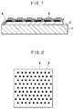
- Fig. 1 is a cross-sectional view of a liquid crystal element along the interface of an electrode, according to an embodiment of the present invention.
- Fig. 2 is a plan view showing an example of an insulation layer arrangement pattern on an electrode of a liquid crystal element according to the present invention.
- Fig. 3 is a plan view showing another example of an insulation layer arrangement pattern on an electrode of a liquid crystal element according to the present invention.
- Fig. 4 is a cross-sectional view of a liquid crystal element along the interface of an electrode, according to another embodiment of the present invention.
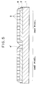
- Fig. 5 is a cross-sectional view of a liquid crystal element along the interface of an electrode, according to still another embodiment of the present invention.
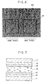
- Fig. 6 is a plan view showing an example of an insulation fiber arrangement pattern on an electrode of a liquid crystal element according to an embodiment of the present invention.
- Fig. 7 is a constitutional view of a conventional liquid crystal element.
- the liquid crystal for use in the present invention is preferably a chiral smectic liquid crystal exhibiting the ferroelectricity, suitably in the chiral smectic C phase (SmC*) or H phase (SmH*), further SmI*, SmF*, or SmG*.
- SmC* chiral smectic C phase
- SmH* H phase
- other liquid crystals useful within a range of the element constitution according to the present invention will also offer sufficient effects as will be described below.
- heat control may be performed to hold it in a desired temperature range.
- a cell is constituted by using an organic film made of, for example, polyimide, polypyrrole, polyvinylalcohol for an orientation layer.
- an organic film made of, for example, polyimide, polypyrrole, polyvinylalcohol for an orientation layer.
- Fig. 1 is a first embodiment of the present invention.
- the same figure shows a cross section of a pixel on the substrate on one side of liquid crystal element.
- This element is fabricated by, for example, providing a transparent electrode 2 (1200 ⁇ ) such as ITO on a glass substrate 1 and forming an insulation material 3 into a pattern sufficiently minute relative to the pixel as shown in the figure. Thereafter, to orient the chiral smectic liquid crystal, columns 4 are formed as shown by SiO oblique vapor deposition, for example.
- This pattern is desirably formed over an entire area of the pixel although the shape of pattern may be arbitrary. For example, a pattern as shown in Fig. 2 or Fig. 3 can be formed.
- Fig. 2 shows an island pattern
- Fig. 3 shows a lattice pattern.
- the insulation material 3 is made by forming a 300 ⁇ film of polyimide by spinner coating, and patterning it in a photolithography process.
- the pattern is formed as large as about 0.4 ⁇ m in line width by using a lattice pattern mask as shown in Fig. 3.
- This line width is sufficiently larger than the diameter of a column made by SiO oblique vapor deposition.
- Fig. 4 shows another embodiment of the present invention.
- the same figure shows a cross section of a pixel on a substrate on one side of a liquid crystal.
- This element is made by forming a film of a transparent electrode 2 such as ITO, about 1000 to 1500 ⁇ thick, on a glass substrate 1 by reactive sputtering, retaining the substrate surface at a temperature of 150 to 300 °C in an oxygen atmosphere (about 10 ⁇ 3 to 10 ⁇ 5 Torr), and EB drawing a desired pattern.
- the insulation portion can be provided at positions of a lattice pattern 0.5 to 0.1 ⁇ m wide, as shown in Fig. 3.
- columns 4 are formed thereon by SiO oblique vapor deposition to orient FLC.
- Fig. 5 shows the constitution of an element according to another embodiment of the present invention in a cross section of two pixels on a substrate on one side of a liquid crystal.
- This element is made by forming a film of a transparent electrode 2 such as ITO, about 1000 to 1500 ⁇ thick, on a glass substrate 1 by reactive sputtering, spinner coating thereon a conductive orientation film 4 of polysiloxane polymer having ultrafine particles of SnO2-Sb dispersed thereto and baking it at about 150 °C to form the film having a thickness of 500 to 1000 ⁇ .
- a transparent electrode 2 such as ITO
- polysiloxane type conductive film 4 is subjected to a rubbing treatment to provide a gap of 1.3 ⁇ m to allow rubbed face to be oriented inwards, into which FLC is injected in vacuum.
- the conductive polymer 4 is formed as a film by the spinner coating collectively over a liquid crystal panel, so that a conductive polymer layer 4' is also formed between pixels to allow for the film formation, as shown in the figure.
- These conductive polymer layers 4, 4' are formed into a lattice pattern as shown in Fig. 3 by partially disconnecting the polymer bonding by electron beam to make the isolation.
- the lattice width is about 0.1 to 0.6 ⁇ m.
- the conductive polymer for use may be polypyrrole which is normally used, in addition to the above cited polymers.
- the substrate heating e.g., 100 to 350 °C
- a laser may be used, rather than the electron beam.
- the chiral smectic liquid crystal and electrode interface are in good conduction, and transversal expansion of domain is prevented or suppressed by the insulation layer portion formed in the conductive polymer film, so that the stable half tone can be formed.
- a conductive polymer is used as an orientation layer, without providing oblique vapor deposited columns as shown in the previous embodiment as the orientation layer, the movement of charges between pixels may also occur as shown in Fig. 5, thereby possibly causing a crosstalk.
- pixels are disconnected in a patterning process for forming the insulation portion in the conductive polymer. Thereby, a problem such as crosstalk can be solved.
- Another embodiment is such that the insulation portion is provided on a conductive polymer by the same method as in the embodiment of Fig. 5, comparted into a minute lattice within a pixel, and formed thereon with columns by SiO oblique vapor deposition for controlling the orientation. With such a constitution, the same effects as in the previous embodiment of Fig. 5 can be obtained.
- Fig. 6 shows an electrode surface of adjacent two pixels, in which an ITO electrode 1000 to 1500 ⁇ thick is formed in the same process as in the above embodiment, and bonded with "Floropoa” (trade name) manufactured by Sumitomo Electric Industries, Ltd., and the insulation portion for preventing the transversal spreading of charges within a pixel and between pixels is provided. Further, SiO columns are formed thereon by SiO oblique vapor deposition as a layer for orienting the FLC.
- Floropoa is manufactured by a process of compacting a powder of polytetrafluoroethylene, and drawing it rapidly under the specific conditions to produce a porous member having a structure of very fine fibers called fibrils in varying dimensions such as the thickness of fiber being 0.01 to 5 ⁇ m, and the pore diameter being 0.02 to 15 ⁇ m, for example.
- a high-gradation optical element with 256 gradations uses Floropoa having a fiber thickness of less than 0.1 ⁇ m, and a pore diameter of less than 5 ⁇ m.
- the portion surrounded by the square frame in Fig. 6 is an electrode 61, which defines one pixel.
- the structure of fine lines in Fig. 6 is a fiber structural member as indicated by numeral 62, with the void portion being a pore portion constituting the porous member having a pore diameter of 0.02 to 15 ⁇ m.
Landscapes
- Physics & Mathematics (AREA)
- Nonlinear Science (AREA)
- Mathematical Physics (AREA)
- Chemical & Material Sciences (AREA)
- Crystallography & Structural Chemistry (AREA)
- General Physics & Mathematics (AREA)
- Optics & Photonics (AREA)
- Liquid Crystal (AREA)
- Liquid Crystal Substances (AREA)
Applications Claiming Priority (2)
| Application Number | Priority Date | Filing Date | Title |
|---|---|---|---|
| JP34856691 | 1991-12-06 | ||
| JP348566/91 | 1991-12-06 |
Publications (2)
| Publication Number | Publication Date |
|---|---|
| EP0545733A1 true EP0545733A1 (de) | 1993-06-09 |
| EP0545733B1 EP0545733B1 (de) | 1997-04-16 |
Family
ID=18397884
Family Applications (1)
| Application Number | Title | Priority Date | Filing Date |
|---|---|---|---|
| EP92311105A Expired - Lifetime EP0545733B1 (de) | 1991-12-06 | 1992-12-04 | Optisches Flüssigkristall-Element |
Country Status (5)
| Country | Link |
|---|---|
| US (2) | US5270844A (de) |
| EP (1) | EP0545733B1 (de) |
| JP (1) | JPH05241138A (de) |
| AT (1) | ATE151893T1 (de) |
| DE (1) | DE69219078T2 (de) |
Cited By (2)
| Publication number | Priority date | Publication date | Assignee | Title |
|---|---|---|---|---|
| GB2289951A (en) * | 1994-05-31 | 1995-12-06 | Samsung Display Devices Co Ltd | Liquid crystal display |
| EP1094439A3 (de) * | 1999-10-20 | 2002-04-17 | Pioneer Corporation | Flüssigkristallanzeigetafel |
Families Citing this family (13)
| Publication number | Priority date | Publication date | Assignee | Title |
|---|---|---|---|---|
| US5327272A (en) * | 1991-03-27 | 1994-07-05 | Canon Kabushiki Kaisha | Optical modulation element |
| JP3100014B2 (ja) * | 1991-12-10 | 2000-10-16 | キヤノン株式会社 | 強誘電性液晶素子及び該素子の製造方法 |
| US5594571A (en) * | 1991-12-10 | 1997-01-14 | Canon Kabushiki Kaisha | Ferroelectric liquid crystal device and process for production thereof |
| US5467209A (en) * | 1992-01-24 | 1995-11-14 | Canon Kabushiki Kaisha | Ferroelectric liquid crystal device with particular layer thicknesses at non-pixel portions and pixel portions |
| US5465169A (en) * | 1992-08-25 | 1995-11-07 | Canon Kabushiki Kaisha | Ferroelectric liquid crystal device with electroconductive protective film and electroconductive alignment film |
| JP3456493B2 (ja) * | 1992-10-24 | 2003-10-14 | ソニー株式会社 | 液晶素子 |
| US5446570A (en) * | 1993-04-27 | 1995-08-29 | Canon Kabushiki Kaisha | Liquid crystal display with projecting portions on the electrodes |
| EP0695965B1 (de) * | 1994-08-04 | 2002-04-10 | Canon Kabushiki Kaisha | Flüssigkristallvorrichtung |
| US5706064A (en) * | 1995-03-31 | 1998-01-06 | Kabushiki Kaisha Toshiba | LCD having an organic-inorganic hybrid glass functional layer |
| US6181397B1 (en) * | 1997-04-01 | 2001-01-30 | Dai Nippon Printing Co., Ltd. | Reflection-type liquid crystal display panel and method of fabricating the same |
| US20060044500A1 (en) * | 2004-08-31 | 2006-03-02 | Canon Kabushiki Kaisha | Organic thin film, method of producing the same, and field effect transistor using the same |
| US7777848B2 (en) * | 2006-03-02 | 2010-08-17 | Canon Kabushiki Kaisha | Manufacturing method of liquid crystal panel and deuterium oxide surface treatment method of alignment film |
| KR102715825B1 (ko) * | 2019-12-13 | 2024-10-11 | 케이제이 케미칼즈 가부시키가이샤 | 광중합 개시제 |
Citations (1)
| Publication number | Priority date | Publication date | Assignee | Title |
|---|---|---|---|---|
| US4765720A (en) * | 1986-07-22 | 1988-08-23 | Canon Kabushiki Kaisha | Method and apparatus for driving ferroelectric liquid crystal, optical modulation device to achieve gradation |
Family Cites Families (17)
| Publication number | Priority date | Publication date | Assignee | Title |
|---|---|---|---|---|
| JPS602650B2 (ja) * | 1980-06-26 | 1985-01-23 | シャープ株式会社 | 液晶セル |
| US4561725A (en) * | 1983-02-09 | 1985-12-31 | Canon Kabushiki Kaisha | Electro-optical device having homogeneous alignment layer hardened with cross-linking agents |
| US4655561A (en) * | 1983-04-19 | 1987-04-07 | Canon Kabushiki Kaisha | Method of driving optical modulation device using ferroelectric liquid crystal |
| JPS60144721A (ja) * | 1984-01-06 | 1985-07-31 | Canon Inc | 画像形成装置 |
| US4712877A (en) * | 1985-01-18 | 1987-12-15 | Canon Kabushiki Kaisha | Ferroelectric display panel of varying thickness and driving method therefor |
| US4832466A (en) * | 1985-04-13 | 1989-05-23 | Canon Kabushiki Kaisha | Optical element |
| US4900135A (en) * | 1985-04-13 | 1990-02-13 | Canon Kabushiki Kaisha | Optical element |
| JP2654940B2 (ja) * | 1985-12-24 | 1997-09-17 | キヤノン株式会社 | 電気光学素子の製造方法 |
| US4796980A (en) * | 1986-04-02 | 1989-01-10 | Canon Kabushiki Kaisha | Ferroelectric liquid crystal optical modulation device with regions within pixels to initiate nucleation and inversion |
| NL8700627A (nl) * | 1987-03-17 | 1988-10-17 | Philips Nv | Werkwijze voor het besturen van een vloeibaar kristalweergeefinrichting en bijbehorende weergeefinrichting. |
| US5122888A (en) * | 1987-07-10 | 1992-06-16 | Canon Kabushiki Kaisha | Focusing plate having phase grating formed by using liquid crystal |
| FR2618587B1 (fr) * | 1987-07-20 | 1992-04-24 | Commissariat Energie Atomique | Ecran a cristal liquide, a electrodes opacifiees dans la zone non commutable de l'ecran et procedes d'obtention d'espaceurs et de traitement de cet ecran |
| DE68929393T2 (de) * | 1988-06-23 | 2002-08-29 | Canon K.K., Tokio/Tokyo | Flüssigkristallvorrichtung |
| JP2756978B2 (ja) * | 1988-08-04 | 1998-05-25 | キヤノン株式会社 | 液晶セル |
| JPH02216128A (ja) * | 1989-02-17 | 1990-08-29 | Seiko Epson Corp | 液晶表示体用透明基板 |
| JP2535414B2 (ja) * | 1989-07-04 | 1996-09-18 | シャープ株式会社 | 液晶表示装置 |
| JP2805253B2 (ja) * | 1990-03-20 | 1998-09-30 | キヤノン株式会社 | 強誘電性液晶装置 |
-
1992
- 1992-11-27 JP JP4339509A patent/JPH05241138A/ja active Pending
- 1992-12-03 US US07/984,837 patent/US5270844A/en not_active Expired - Fee Related
- 1992-12-04 DE DE69219078T patent/DE69219078T2/de not_active Expired - Fee Related
- 1992-12-04 EP EP92311105A patent/EP0545733B1/de not_active Expired - Lifetime
- 1992-12-04 AT AT92311105T patent/ATE151893T1/de not_active IP Right Cessation
-
1993
- 1993-09-01 US US08/114,397 patent/US5321538A/en not_active Expired - Fee Related
Patent Citations (1)
| Publication number | Priority date | Publication date | Assignee | Title |
|---|---|---|---|---|
| US4765720A (en) * | 1986-07-22 | 1988-08-23 | Canon Kabushiki Kaisha | Method and apparatus for driving ferroelectric liquid crystal, optical modulation device to achieve gradation |
Non-Patent Citations (4)
| Title |
|---|
| HARTMANN W. J. A. M.: "FERROELECTRIC LIQUID-CRYSTAL VIDEO DISPLAY.", PROCEEDINGS OF THE SOCIETY OF INFORMATION DISPLAY, SOCIETY FOR INFORMATION DISPLAY. PLAYA DEL REY, CA., US, vol. 30., no. 02., 1 January 1989 (1989-01-01), US, pages 99 - 103., XP000114030 * |
| PATENT ABSTRACTS OF JAPAN vol. 13, no. 303 (P-896)12 July 1989 & JP-A-01 078 235 ( CANON ) 23 March 1989 * |
| PATENT ABSTRACTS OF JAPAN vol. 14, no. 283 (P-1063)19 June 1990 & JP-A-02 084 619 ( SEIKO ) 26 March 1990 * |
| PATENT ABSTRACTS OF JAPAN vol. 15, no. 287 (P-1229)22 July 1991 & JP-A-03 100 520 ( CANON ) 25 April 1991 * |
Cited By (4)
| Publication number | Priority date | Publication date | Assignee | Title |
|---|---|---|---|---|
| GB2289951A (en) * | 1994-05-31 | 1995-12-06 | Samsung Display Devices Co Ltd | Liquid crystal display |
| US5554419A (en) * | 1994-05-31 | 1996-09-10 | Samsung Display Devices Co., Ltd. | Liquid crystal display device |
| GB2289951B (en) * | 1994-05-31 | 1998-08-26 | Samsung Display Devices Co Ltd | Liquid crystal display device |
| EP1094439A3 (de) * | 1999-10-20 | 2002-04-17 | Pioneer Corporation | Flüssigkristallanzeigetafel |
Also Published As
| Publication number | Publication date |
|---|---|
| US5270844A (en) | 1993-12-14 |
| DE69219078D1 (de) | 1997-05-22 |
| EP0545733B1 (de) | 1997-04-16 |
| ATE151893T1 (de) | 1997-05-15 |
| DE69219078T2 (de) | 1997-09-18 |
| US5321538A (en) | 1994-06-14 |
| JPH05241138A (ja) | 1993-09-21 |
Similar Documents
| Publication | Publication Date | Title |
|---|---|---|
| EP0545733B1 (de) | Optisches Flüssigkristall-Element | |
| US5644372A (en) | Liquid crystal display device having protrusions on the electrodes | |
| EP0240010B1 (de) | Optische Modulationsvorrichtung | |
| US5786879A (en) | Liquid crystal device with different pretilt in peripheral portion | |
| JPH0668589B2 (ja) | 強誘電性液晶素子 | |
| US5812230A (en) | Liquid crystal display and manufacturing method thereof with isotropic microstructural elements between smectic layers | |
| JPH04247428A (ja) | カイラルスメクチック液晶素子 | |
| US6392624B1 (en) | Method of driving liquid crystal device | |
| US5956010A (en) | Liquid crystal apparatus and driving method | |
| JP2981805B2 (ja) | 液晶表示素子 | |
| US6118512A (en) | Manufacturing method of a liquid crystal display element | |
| JPH06167711A (ja) | 強誘電性液晶素子 | |
| JPH11101993A (ja) | 液晶素子、液晶の配向制御方法、及び液晶素子の製造方法 | |
| JPH06308498A (ja) | 強誘電性液晶素子 | |
| JPH0772485A (ja) | 液晶表示素子 | |
| US5258865A (en) | Ferroelectric liquid crystal device | |
| JP2505744B2 (ja) | 電極基板及び光学変調素子の製造法 | |
| JPS63225224A (ja) | 電気光学装置 | |
| JP3329721B2 (ja) | 液晶表示装置 | |
| JPS63228124A (ja) | 液晶電気光学装置 | |
| JPH0588154A (ja) | 強誘電液晶素子 | |
| JPH0728042A (ja) | 光学装置 | |
| JPH07122703B2 (ja) | 光学変調素子 | |
| JPH06202115A (ja) | 液晶表示素子およびそれによる中間調表示方法 | |
| JPH06289351A (ja) | 液晶表示装置の製造方法と液晶表示装置 |
Legal Events
| Date | Code | Title | Description |
|---|---|---|---|
| PUAI | Public reference made under article 153(3) epc to a published international application that has entered the european phase |
Free format text: ORIGINAL CODE: 0009012 |
|
| AK | Designated contracting states |
Kind code of ref document: A1 Designated state(s): AT BE CH DE DK ES FR GB GR IE IT LI LU NL PT SE |
|
| 17P | Request for examination filed |
Effective date: 19931022 |
|
| RIN1 | Information on inventor provided before grant (corrected) |
Inventor name: EGAN, ALISTAIR Inventor name: FONTANA, JAMES A. Inventor name: PALMER, DOUGLAS L. Inventor name: BECK, GREGORY F. Inventor name: MURAKAMI, TOMOKO,C/O CANON KABUSHIKI KAISHA Inventor name: FUJIWARA, RYOJI,C/O CANON KABUSHIKI KAISHA Inventor name: KANEKO, SHUZO,C/O CANON KABUSHIKI KAISHA Inventor name: MARUYAMA, TOMOKO,C/O CANON KABUSHIKI KAISHA |
|
| RIN1 | Information on inventor provided before grant (corrected) |
Inventor name: MURAKAMI, TOMOKO,C/O CANON KABUSHIKI KAISHA Inventor name: FUJIWARA, RYOJI,C/O CANON KABUSHIKI KAISHA Inventor name: KANEKO, SHUZO,C/O CANON KABUSHIKI KAISHA Inventor name: MARUYAMA, TOMOKO,C/O CANON KABUSHIKI KAISHA |
|
| GRAG | Despatch of communication of intention to grant |
Free format text: ORIGINAL CODE: EPIDOS AGRA |
|
| 17Q | First examination report despatched |
Effective date: 19960607 |
|
| GRAH | Despatch of communication of intention to grant a patent |
Free format text: ORIGINAL CODE: EPIDOS IGRA |
|
| GRAH | Despatch of communication of intention to grant a patent |
Free format text: ORIGINAL CODE: EPIDOS IGRA |
|
| GRAA | (expected) grant |
Free format text: ORIGINAL CODE: 0009210 |
|
| AK | Designated contracting states |
Kind code of ref document: B1 Designated state(s): AT BE CH DE DK ES FR GB GR IE IT LI LU NL PT SE |
|
| PG25 | Lapsed in a contracting state [announced via postgrant information from national office to epo] |
Ref country code: NL Effective date: 19970416 Ref country code: LI Effective date: 19970416 Ref country code: IT Free format text: LAPSE BECAUSE OF FAILURE TO SUBMIT A TRANSLATION OF THE DESCRIPTION OR TO PAY THE FEE WITHIN THE PRE;WARNING: LAPSES OF ITALIAN PATENTS WITH EFFECTIVE DATE BEFORE 2007 MAY HAVE OCCURRED AT ANY TIME BEFORE 2007. THE CORRECT EFFECTIVE DATE MAY BE DIFFERENT FROM THE ONE RECORDED.SCRIBED TIME-LIMIT Effective date: 19970416 Ref country code: GR Free format text: LAPSE BECAUSE OF FAILURE TO SUBMIT A TRANSLATION OF THE DESCRIPTION OR TO PAY THE FEE WITHIN THE PRESCRIBED TIME-LIMIT Effective date: 19970416 Ref country code: ES Free format text: THE PATENT HAS BEEN ANNULLED BY A DECISION OF A NATIONAL AUTHORITY Effective date: 19970416 Ref country code: DK Effective date: 19970416 Ref country code: CH Effective date: 19970416 Ref country code: BE Effective date: 19970416 Ref country code: AT Effective date: 19970416 |
|
| REF | Corresponds to: |
Ref document number: 151893 Country of ref document: AT Date of ref document: 19970515 Kind code of ref document: T |
|
| REG | Reference to a national code |
Ref country code: CH Ref legal event code: EP |
|
| REF | Corresponds to: |
Ref document number: 69219078 Country of ref document: DE Date of ref document: 19970522 |
|
| PG25 | Lapsed in a contracting state [announced via postgrant information from national office to epo] |
Ref country code: SE Effective date: 19970716 Ref country code: PT Effective date: 19970716 |
|
| ET | Fr: translation filed | ||
| REG | Reference to a national code |
Ref country code: IE Ref legal event code: FG4D Free format text: 73290 |
|
| NLV1 | Nl: lapsed or annulled due to failure to fulfill the requirements of art. 29p and 29m of the patents act | ||
| REG | Reference to a national code |
Ref country code: CH Ref legal event code: PL |
|
| PG25 | Lapsed in a contracting state [announced via postgrant information from national office to epo] |
Ref country code: LU Free format text: LAPSE BECAUSE OF NON-PAYMENT OF DUE FEES Effective date: 19971204 Ref country code: IE Free format text: LAPSE BECAUSE OF NON-PAYMENT OF DUE FEES Effective date: 19971204 |
|
| PLBE | No opposition filed within time limit |
Free format text: ORIGINAL CODE: 0009261 |
|
| 26N | No opposition filed | ||
| REG | Reference to a national code |
Ref country code: GB Ref legal event code: IF02 |
|
| PGFP | Annual fee paid to national office [announced via postgrant information from national office to epo] |
Ref country code: GB Payment date: 20041122 Year of fee payment: 13 |
|
| PGFP | Annual fee paid to national office [announced via postgrant information from national office to epo] |
Ref country code: FR Payment date: 20041220 Year of fee payment: 13 |
|
| PGFP | Annual fee paid to national office [announced via postgrant information from national office to epo] |
Ref country code: DE Payment date: 20050217 Year of fee payment: 13 |
|
| PG25 | Lapsed in a contracting state [announced via postgrant information from national office to epo] |
Ref country code: GB Free format text: LAPSE BECAUSE OF NON-PAYMENT OF DUE FEES Effective date: 20051204 |
|
| PG25 | Lapsed in a contracting state [announced via postgrant information from national office to epo] |
Ref country code: DE Free format text: LAPSE BECAUSE OF NON-PAYMENT OF DUE FEES Effective date: 20060701 |
|
| GBPC | Gb: european patent ceased through non-payment of renewal fee |
Effective date: 20051204 |
|
| PG25 | Lapsed in a contracting state [announced via postgrant information from national office to epo] |
Ref country code: FR Free format text: LAPSE BECAUSE OF NON-PAYMENT OF DUE FEES Effective date: 20060831 |
|
| REG | Reference to a national code |
Ref country code: FR Ref legal event code: ST Effective date: 20060831 |