EP0601780A2 - Digitaler programmierbarer Frequenzgenerator - Google Patents
Digitaler programmierbarer Frequenzgenerator Download PDFInfo
- Publication number
- EP0601780A2 EP0601780A2 EP93309598A EP93309598A EP0601780A2 EP 0601780 A2 EP0601780 A2 EP 0601780A2 EP 93309598 A EP93309598 A EP 93309598A EP 93309598 A EP93309598 A EP 93309598A EP 0601780 A2 EP0601780 A2 EP 0601780A2
- Authority
- EP
- European Patent Office
- Prior art keywords
- frequency
- transistors
- ring
- ring oscillator
- power supply
- Prior art date
- Legal status (The legal status is an assumption and is not a legal conclusion. Google has not performed a legal analysis and makes no representation as to the accuracy of the status listed.)
- Granted
Links
- 230000005669 field effect Effects 0.000 claims abstract description 4
- 239000013078 crystal Substances 0.000 claims description 15
- 230000010355 oscillation Effects 0.000 claims description 4
- 239000004020 conductor Substances 0.000 claims 2
- 238000000034 method Methods 0.000 abstract description 14
- 238000010420 art technique Methods 0.000 abstract description 2
- 238000005516 engineering process Methods 0.000 description 7
- 238000013461 design Methods 0.000 description 5
- 238000013459 approach Methods 0.000 description 3
- 230000000295 complement effect Effects 0.000 description 2
- 238000010586 diagram Methods 0.000 description 2
- 229910001218 Gallium arsenide Inorganic materials 0.000 description 1
- 230000015572 biosynthetic process Effects 0.000 description 1
- 238000007796 conventional method Methods 0.000 description 1
- 238000013479 data entry Methods 0.000 description 1
- 230000003247 decreasing effect Effects 0.000 description 1
- 230000001419 dependent effect Effects 0.000 description 1
- 230000007613 environmental effect Effects 0.000 description 1
- 238000011156 evaluation Methods 0.000 description 1
- 230000006870 function Effects 0.000 description 1
- 230000002452 interceptive effect Effects 0.000 description 1
- 230000008520 organization Effects 0.000 description 1
- 230000001902 propagating effect Effects 0.000 description 1
- 238000005070 sampling Methods 0.000 description 1
- 238000004513 sizing Methods 0.000 description 1
- 238000003786 synthesis reaction Methods 0.000 description 1
Images
Classifications
-
- H—ELECTRICITY
- H03—ELECTRONIC CIRCUITRY
- H03L—AUTOMATIC CONTROL, STARTING, SYNCHRONISATION OR STABILISATION OF GENERATORS OF ELECTRONIC OSCILLATIONS OR PULSES
- H03L7/00—Automatic control of frequency or phase; Synchronisation
- H03L7/06—Automatic control of frequency or phase; Synchronisation using a reference signal applied to a frequency- or phase-locked loop
- H03L7/08—Details of the phase-locked loop
- H03L7/099—Details of the phase-locked loop concerning mainly the controlled oscillator of the loop
- H03L7/0995—Details of the phase-locked loop concerning mainly the controlled oscillator of the loop the oscillator comprising a ring oscillator
-
- H—ELECTRICITY
- H03—ELECTRONIC CIRCUITRY
- H03K—PULSE TECHNIQUE
- H03K3/00—Circuits for generating electric pulses; Monostable, bistable or multistable circuits
- H03K3/02—Generators characterised by the type of circuit or by the means used for producing pulses
- H03K3/027—Generators characterised by the type of circuit or by the means used for producing pulses by the use of logic circuits, with internal or external positive feedback
- H03K3/03—Astable circuits
- H03K3/0315—Ring oscillators
Definitions
- the present invention relates to a digital programmable frequency generator.
- Frequency generators that may be programmed are utilized in a wide variety of applications. Typical applications include radio and television receivers and transmitters, and computer devices that must operate at different clock rates, or be compatible with systems that operate at different clock rates.
- a typical prior-art technique for implementing a programmable frequency generator is the use of a phase-locked loop (PLL).
- the PLL includes a voltage-controlled oscillator (VCO), phase comparator, and programmable counter that are arranged in a well-known configuration. By changing the count of the counter, a desired frequency division ratio can be achieved that produces the desired output frequency from the VCO.
- VCO voltage-controlled oscillator
- phase comparator phase comparator
- programmable counter programmable counter that are arranged in a well-known configuration. By changing the count of the counter, a desired frequency division ratio can be achieved that produces the desired output frequency from the VCO.
- a PLL has an inherent limitation as to the speed that a change in frequency can be made, which is dependent on the loop characteristics
- PLL implementations require significant power to operate, and their analog nature makes them susceptible to noise problems.
- PLL designs are not readily adapted to low-voltage operation, as may occur, for example, in battery-operated portable systems where 3 volt (or less) operation is becoming common.
- DDS direct digital synthesis
- a digital representation of an analog waveform for example a sinusoid
- By repetitively reading out the memory at a given rate, and applying the digital waveform to a digital-to-analog converter, an analog waveform at the desired frequency is obtained.
- the DDS technique typically allows for relatively rapid changes in frequency.
- DDS is overly complicated for many applications, as when only a binary clock waveform is needed, for example. It also may not lend itself to low-voltage, low-power applications.
- Another approach that is more oriented to digital technology involves the use of a ring oscillator with multiple inverter stages. The number of active stages is changed, in order to change the frequency of oscillation. However, that may require a large number of inverter stages to obtain a wide frequency range, especially if relatively small steps in frequency are required over the range.
- a ring oscillator receives at least one operating voltage through a programmable array of field effect transistors. Digitally selecting a given set of the transistors provides a given operating current for the ring, which establishes the frequency of operation.
- the technique is implemented in a CMOS integrated circuit.
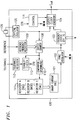
- Fig. 1 shows a block diagram of a clock generator that advantageously uses the present technique.
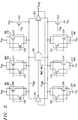
- Fig. 2 shows a ring oscillator implementing the inventive technique.
- the PFG may be used to produce a highly accurate variable frequency system clock.
- the frequency ranges from 400 kHz to 100 MHz, while using a single inexpensive crystal oscillator as a reference. Both the frequency and tolerance of the PFG can be programmed by the user. Power consumption is of concern in many systems, especially portable battery-operated systems. Two methods that can be used to minimize system power are to deactivate the system when not in use, and to vary the clock rate to match the work load or application.
- the PFG described herein meets both of these objectives.
- the PFG can stop the clock in a known state when the system is idle.
- the PFG may switch its output frequency rapidly (e.g., in less than 150 microseconds in the illustrative embodiment), without stopping the output.
- a block diagram of a typical system utilizing the present invention is shown. While the overall organization of this system is otherwise similar to those known in the art, it will be seen that the binary current tree 101, ring oscillator 102, and ring frequency registers 111 provides for a unique design and method of operation, as described below.
- the PFG can be used as a stand-alone integrated circuit chip, or implemented as a macro cell in a microprocessor or system management device.
- the PFG can be understood with reference to five major functional areas: a ring oscillator and binary current tree, frequency controller, frequency divider, output clock generator, and control logic.
- inputs are provided for programming the reference frequency register 109 and frequency divider stage 103, while two bond pads provide for connection to an external crystal 106.
- the core of the PFG is a binary current tree 101 and a ring oscillator 102, which employs a digital frequency feedback loop to generate a stabilized output at the specified frequency.
- the ring oscillator includes a ring of an odd number of inverters 201, 202, and 203, considering that NAND gate 202 performs an inversion when RING ON is high.
- These inverters receive positive (V DDR ) and negative (V SSR ) power supply voltages through the binary current tree, which is voltage controlled in the illustrative case.
- This current tree includes PMOS and NMOS transistor networks, each arranged in three banks (204, 210, 216, and 207, 213, 219, respectively).
- the PMOS and NMOS transistor networks limit current to the ring and thereby control the delay through each inverter. This in turn alters the frequency in the following manner: when all the transistors in the binary current tree are on (conducting), the frequency of oscillation of the ring oscillator is maximum. When a given pair of p-channel and n-channel transistors is turned off (non-conducting), the power supply current to the ring is thereby reduced, which reduces the frequency of oscillation. If all the controlled transistors are turned off, a minimum frequency of operation is maintained by current through transistors 222 and 223.
- the ring may be turned on or off by the RING ON signal (from control logic 114) applied to NAND gate 202. This allows, for example, retaining the crystal oscillator on while disabling the ring oscillator in order to save power.
- Each pair of banks is tuned so that the oscillator frequency changes in uniform steps when turning on/off transistor pairs within a pair of banks. For example, applying a low voltage to the gate of transistor 205 while simultaneously applying a high voltage to the gate of transistor 208 turns on that pair, allowing power supply current conduction therethrough to the ring oscillator.
- the low and high gate voltages may be V SS and V DD .
- a wider range of the ring oscillator frequency may be obtained by using V SSR and V DDR for the low and high voltages on the gates of the transistors in the binary current tree.
- the transistor sizes in the banks are designed to give varying sized steps (small, medium and large), with overlap between banks to ensure frequency convergence.
- the BIG and SML banks (204, 207, 216 and 219) each have 16 transistors, whereas the MED banks (210 and 213) each have 20 transistors.
- Overlap in frequency may be obtained by sizing the transistors such that the current supplied by one BIG transistor pair is equal to the current supplied by less than all of the MED transistor pairs.
- the current produced by a BIG transistor pair is equal to the current provided by 16 MED transistor pairs.
- the transistors in the banks are controlled by the ring frequency registers 111 according to signals generated by the comparator 110.
- the REGISTER A provides the control signals to the gates of the transistors in banks 204 and 207, whereas REGISTERS B and C similarly control the other banks as indicated in Fig. 1.
- the number of "on" transistor pairs is increased/decreased by one, or alternatively unchanged, during each evaluation of the ring frequency.
- the ring oscillator frequency is sampled and periodically adjusted; e.g., every 1 to 2 microseconds in the illustrative case.
- the frequency controller comprises the reference frequency generator, being crystal oscillator 105, the gated counter 108, the reference frequency register 109, the comparator 110, the ring frequency registers 111, and the stability checker 112.
- the frequency controller serves to measures the frequency of the ring oscillator, and send the appropriate control signals to the binary current tree to obtain (or maintain) the desired ring oscillator frequency.
- the gated counter 108 counts the number of cycles of the ring oscillator during a known interval, which is a function of the crystal 106 connected to the crystal oscillator 105.
- the gated counter is pre-loaded with the one's complement of the desired count from the reference frequency register 109. The counter then counts up during the sampling interval.
- comparator 110 determines whether the ring frequency should be changed and in what direction (faster or slower). For this purpose, comparator 110 provides "up”, “down”, and “equal” signal outputs to the ring frequency registers 111.
- the stability checker 112 monitors the magnitude of the difference between the set frequency and the actual frequency. This difference is used to determine whether the ring oscillator is stable and within the desired tolerance (e.g., from 0.5% to 4% in the illustrative case), as programmed into the tolerance register 113.
- the tolerance/stability check circuit may be used to adapt the PFG to environmental conditions and specifications. For example, if the usage is in a high-noise system, the tolerance can be increased in value (i.e., loosened).
- the frequency of the ring oscillator is influenced by the programmed tolerance. For example, a looser tolerance (less accuracy) requirement allows for a lower ROSC frequency (f ring ), which reduces power dissipation.
- the stability checker sends a signal STB to the control logic 114 when the ring oscillator is stable. If a change in ring frequency is required such that a large step size transistor must be turned on/off, the stable signal is dropped to prevent any large variation in ring frequency from propagating to the output.
- the divide-by-N frequency divider 103 divides the ring oscillator output down to a lower frequency.
- the frequency divider 103 is typically designed so that the programmable frequency output is step-wise continuous over the entire programmable range. That is, the frequency output is quantized (for example, in steps of approximately 0.5%) over the output frequency range (for example, 20 kHz to 100 MHz).
- the divider 103 in the illustrative case consists of a divide by 2-or-3 followed by a chain of divide-by-2 blocks. To minimize power dissipation, the divide-by-2 chain may be a ripple counter and unneeded portions of the chain (higher order bits) are inactive.
- N (2 or 3) ⁇ 2 L , where L typically ranges from 0 to 6.
- the output clock generator 104 receives source selection information from the control logic 114 and input clock sources from the crystal oscillator and the frequency divider. It includes an input multiplexer and output formatter (not shown). The input multiplexer is designed to allow the output frequency to be switched without a glitch. To switch from the crystal oscillator 105 to the frequency divider 103, the multiplexer control signal disables the crystal oscillator signal path and enables the frequency divider path after 2 clock cycles from the frequency divider. A complementary sequence occurs when switching from the frequency divider to the crystal oscillator.
- the formatter is able to produce variously formatted clock outputs (e.g., 2-phase, 4-phase, etc.) In addition, this block halts the output in a predetermined state. This corresponds to the very low power stopped clock mode.
- the control logic 114 continuously monitors the signals within the PFG as well as the input control signals. In the power-up mode, the output clock generator 104 is instructed to use the crystal oscillator 105 as the clock. When the PFG register is updated, the control logic checks to see if the ring oscillator is required for operation. If so, the ring is turned on and the control logic waits for the frequency controller to set the stability check signal. While waiting for the stability signal to be set, the output clock generation may continue using the crystal oscillator as the source clock. When stability is achieved, the output clock generator is instructed to use the output of the frequency divider 103 as the clock source. If the control logic senses loss of stability, it instructs the output clock generator to use the crystal oscillator clock until the frequency controller once again determines that stability is achieved.
- Fig. 1 is illustrative of a clock generator
- the binary-controlled ring oscillator as shown illustratively in Fig. 2 may be used in a variety of other applications, as will be apparent to persons of skill in the art.
- the number of stages in the ring oscillator, and the number and grouping of transistors in the binary current tree may differ from those shown herein.
- Various implementations of the digital feedback loop are possible.
- the present technique may be used in applications that do not require a feedback loop nor reference frequency.
- the above embodiment has been illustrated in CMOS technology, other technologies are possible.
- a single conductivity type of transistor may be used to control the current flow from only a single power supply voltage, allowing for designs with only n-channel transistors in NMOS technology, or alternatively only p-channel transistors in PMOS technology, for example.
- Applications in bipolar technologies, including those that implement GaAs and various other device types, are also possible and included herein. In the bipolar case, the binary current tree is typically current controlled, rather than voltage controlled.
Landscapes
- Stabilization Of Oscillater, Synchronisation, Frequency Synthesizers (AREA)
- Oscillators With Electromechanical Resonators (AREA)
Applications Claiming Priority (2)
| Application Number | Priority Date | Filing Date | Title |
|---|---|---|---|
| US987917 | 1992-12-08 | ||
| US07/987,917 US5416446A (en) | 1992-12-08 | 1992-12-08 | Digital programmable frequency generator |
Publications (3)
| Publication Number | Publication Date |
|---|---|
| EP0601780A2 true EP0601780A2 (de) | 1994-06-15 |
| EP0601780A3 EP0601780A3 (de) | 1995-01-18 |
| EP0601780B1 EP0601780B1 (de) | 1999-04-14 |
Family
ID=25533691
Family Applications (1)
| Application Number | Title | Priority Date | Filing Date |
|---|---|---|---|
| EP93309598A Expired - Lifetime EP0601780B1 (de) | 1992-12-08 | 1993-12-01 | Digitaler programmierbarer Frequenzgenerator |
Country Status (4)
| Country | Link |
|---|---|
| US (1) | US5416446A (de) |
| EP (1) | EP0601780B1 (de) |
| JP (1) | JP2912148B2 (de) |
| DE (1) | DE69324451T2 (de) |
Cited By (14)
| Publication number | Priority date | Publication date | Assignee | Title |
|---|---|---|---|---|
| GB2296612A (en) * | 1994-12-31 | 1996-07-03 | Hyundai Electronics Ind | Low power ring oscillator for bias generator |
| FR2750268A1 (fr) * | 1996-06-19 | 1997-12-26 | Bull Sa | Procede pour obtenir un signal a frequence variable et cellule a retard variable adaptee a la mise en oeuvre de ce procede |
| FR2852749A1 (fr) * | 2003-03-18 | 2004-09-24 | Suisse Electronique Microtech | Diviseur de frequence a taux de division variable |
| US7064617B2 (en) | 2003-05-02 | 2006-06-20 | Silicon Laboratories Inc. | Method and apparatus for temperature compensation |
| WO2006118284A1 (en) * | 2005-04-27 | 2006-11-09 | Semiconductor Energy Laboratory Co., Ltd. | Pll circuit and semiconductor device having the same |
| US7187241B2 (en) | 2003-05-02 | 2007-03-06 | Silicon Laboratories Inc. | Calibration of oscillator devices |
| US7288998B2 (en) | 2003-05-02 | 2007-10-30 | Silicon Laboratories Inc. | Voltage controlled clock synthesizer |
| US7295077B2 (en) | 2003-05-02 | 2007-11-13 | Silicon Laboratories Inc. | Multi-frequency clock synthesizer |
| EP1916768A1 (de) * | 2006-10-27 | 2008-04-30 | Interuniversitair Micro-Elektronica Centrum Vzw | Vorrichtung und Verfahren zur Erzeugung eines Signals mit beim Start vordefiniertem Transienten |
| EP1916769A1 (de) * | 2006-10-27 | 2008-04-30 | Interuniversitair Microelektronica Centrum | Vorrichtung und Verfahren zur Erzeugung eines Signals mit beim Start vordefiniertem Transienten |
| US7436227B2 (en) | 2003-05-02 | 2008-10-14 | Silicon Laboratories Inc. | Dual loop architecture useful for a programmable clock source and clock multiplier applications |
| US7719373B2 (en) | 2006-10-27 | 2010-05-18 | Imec | Device and method for generating a signal with predefined transcient at start-up |
| WO2011008999A1 (en) * | 2009-07-16 | 2011-01-20 | Qualcomm Incorporated | Frequency divider with a configurable dividing ratio |
| US11115005B2 (en) | 2019-08-28 | 2021-09-07 | Samsung Electronics Co., Ltd | Ring voltage controlled oscillator (VCO) startup helper circuit |
Families Citing this family (29)
| Publication number | Priority date | Publication date | Assignee | Title |
|---|---|---|---|---|
| US5479129A (en) * | 1993-11-24 | 1995-12-26 | At&T Corp. | Variable propagation delay digital signal inverter |
| US5592129A (en) * | 1995-06-22 | 1997-01-07 | National Semiconductor Corporation | High resolution, large multiplication factor digitally-controlled frequency multiplier |
| US5694308A (en) * | 1995-07-03 | 1997-12-02 | Motorola, Inc. | Method and apparatus for regulated low voltage charge pump |
| US5565817A (en) * | 1995-07-31 | 1996-10-15 | Lucent Technologies Inc. | Ring oscillator having accelerated charging and discharging of capacitors |
| US5739725A (en) * | 1996-01-29 | 1998-04-14 | International Business Machines Corporation | Digitally controlled oscillator circuit |
| US5796313A (en) * | 1996-04-25 | 1998-08-18 | Waferscale Integration Inc. | Low power programmable ring oscillator |
| JPH10201222A (ja) * | 1996-12-27 | 1998-07-31 | Fujitsu Ltd | 昇圧回路及びこれを用いた半導体装置 |
| US6028462A (en) * | 1997-08-22 | 2000-02-22 | Lsi Logic Corporation | Tunable delay for very high speed |
| US6008680A (en) * | 1997-08-27 | 1999-12-28 | Lsi Logic Corporation | Continuously adjustable delay-locked loop |
| US5952892A (en) * | 1997-09-29 | 1999-09-14 | Lsi Logic Corporation | Low-gain, low-jitter voltage controlled oscillator circuit |
| US6072372A (en) * | 1997-11-07 | 2000-06-06 | Oki Electric Industry Co., Ltd. | Ring-type voltage-controlled oscillator having a sub-frequency band selection circuit |
| US6114915A (en) * | 1998-11-05 | 2000-09-05 | Altera Corporation | Programmable wide-range frequency synthesizer |
| US6671341B1 (en) * | 1999-09-17 | 2003-12-30 | Agere Systems, Inc. | Glitch-free phase switching synthesizer |
| TW527763B (en) * | 2000-05-01 | 2003-04-11 | Koninkl Philips Electronics Nv | Power adaptive frequency divider |
| US7231197B1 (en) * | 2000-10-27 | 2007-06-12 | Fisher Daniel E | Angle rate interferometer and passive ranger |
| US20070259636A1 (en) * | 2000-10-27 | 2007-11-08 | Fisher Daniel E | RF bridge for an angle rate interferometer |
| US20050068118A1 (en) * | 2003-09-30 | 2005-03-31 | Silicon Laboratories, Inc. | Reconfigurable terminal |
| US7148755B2 (en) * | 2003-08-26 | 2006-12-12 | Hewlett-Packard Development Company, L.P. | System and method to adjust voltage |
| KR100587144B1 (ko) * | 2004-04-30 | 2006-06-08 | 매그나칩 반도체 유한회사 | 소비전력 감소을 위한 SoC 칩의 클럭생성장치 |
| TWI400886B (zh) | 2005-02-28 | 2013-07-01 | Semiconductor Energy Lab | 半導體裝置和使用該半導體裝置的電子設備 |
| US20070266263A1 (en) * | 2006-05-11 | 2007-11-15 | Silicon Integrated Systems Corp. | Speed adjustment system and method for performing the same |
| JP4991193B2 (ja) * | 2006-07-04 | 2012-08-01 | 株式会社日立製作所 | 周波数可変発振器 |
| EP2849338A1 (de) * | 2013-09-12 | 2015-03-18 | Fujitsu Semiconductor Limited | Schaltungen, die zur Takterzeugung und Verteilung verwendbar sind |
| US10061336B1 (en) * | 2017-10-29 | 2018-08-28 | Birad—Research & Development Company Ltd. | Switch capacitor in bandgap voltage reference (BGREF) |
| CN114127915B (zh) * | 2019-07-15 | 2025-08-29 | 华为技术有限公司 | 一种检测电路及传感器 |
| US11641206B2 (en) * | 2021-01-07 | 2023-05-02 | AyDeeKay LLC | Digitally calibrated programmable clock phase generation circuit |
| WO2023055388A1 (en) * | 2021-10-01 | 2023-04-06 | Hewlett-Packard Development Company, L.P. | External crystal oscillator cycle duration and variation tracking |
| US11824548B2 (en) * | 2021-12-17 | 2023-11-21 | Xilinx, Inc. | Pulse generator for injection locked oscillator |
| US20250271889A1 (en) * | 2024-02-23 | 2025-08-28 | Taiwan Semiconductor Manufacturing Company, Ltd. | Leakage Insensitive Switch Control for Bandgap Thermal Sensors in Core-MOS Nodes |
Family Cites Families (12)
| Publication number | Priority date | Publication date | Assignee | Title |
|---|---|---|---|---|
| US3287655A (en) * | 1964-11-30 | 1966-11-22 | Douglas A Venn | Digital control for disciplining oscillators |
| US3931588A (en) * | 1974-09-10 | 1976-01-06 | Rca Corporation | Voltage controlled oscillator utilizing field effect transistors |
| US4346343A (en) * | 1980-05-16 | 1982-08-24 | International Business Machines Corporation | Power control means for eliminating circuit to circuit delay differences and providing a desired circuit delay |
| EP0390226A1 (de) * | 1984-07-31 | 1990-10-03 | Yamaha Corporation | Absorptionsschaltung des Zitterns |
| US5111085A (en) * | 1987-04-29 | 1992-05-05 | Ncr Corporation | Digitally controlled delay circuit |
| US4906944A (en) * | 1988-08-17 | 1990-03-06 | Rockwell International Corporation | Integrator controlled time compensated clock oscillator |
| US4988960A (en) * | 1988-12-21 | 1991-01-29 | Yamaha Corporation | FM demodulation device and FM modulation device employing a CMOS signal delay device |
| US5072197A (en) * | 1991-01-03 | 1991-12-10 | Hewlett-Packard Company | Ring oscillator circuit having improved frequency stability with respect to temperature, supply voltage, and semiconductor process variations |
| US5121014A (en) * | 1991-03-05 | 1992-06-09 | Vlsi Technology, Inc. | CMOS delay circuit with controllable delay |
| JPH04351008A (ja) * | 1991-05-28 | 1992-12-04 | Sony Corp | ディジタルvco |
| US5220216A (en) * | 1992-01-02 | 1993-06-15 | Woo Ann K | Programmable driving power of a CMOS gate |
| US5206609A (en) * | 1992-05-15 | 1993-04-27 | Motorola, Inc. | Current controlled oscillator with linear output frequency |
-
1992
- 1992-12-08 US US07/987,917 patent/US5416446A/en not_active Expired - Lifetime
-
1993
- 1993-12-01 DE DE69324451T patent/DE69324451T2/de not_active Expired - Lifetime
- 1993-12-01 EP EP93309598A patent/EP0601780B1/de not_active Expired - Lifetime
- 1993-12-07 JP JP5339865A patent/JP2912148B2/ja not_active Expired - Lifetime
Cited By (26)
| Publication number | Priority date | Publication date | Assignee | Title |
|---|---|---|---|---|
| GB2296612A (en) * | 1994-12-31 | 1996-07-03 | Hyundai Electronics Ind | Low power ring oscillator for bias generator |
| GB2296612B (en) * | 1994-12-31 | 1999-07-21 | Hyundai Electronics Ind | Ring oscillator for semiconductor device |
| FR2750268A1 (fr) * | 1996-06-19 | 1997-12-26 | Bull Sa | Procede pour obtenir un signal a frequence variable et cellule a retard variable adaptee a la mise en oeuvre de ce procede |
| EP0814562A1 (de) * | 1996-06-19 | 1997-12-29 | Bull S.A. | Verfahren zur Erzeugung einer variablen Frequenz und variabele Verzögerungszelle zur Durchführung des Verfahrens |
| US5952891A (en) * | 1996-06-19 | 1999-09-14 | Bull S.A. | Variable delay cell with hysteresis and ring oscillator using same |
| USRE38274E1 (en) * | 1996-06-19 | 2003-10-14 | Bull S.A. | Variable delay cell with hysteresis and ring oscillator using same |
| FR2852749A1 (fr) * | 2003-03-18 | 2004-09-24 | Suisse Electronique Microtech | Diviseur de frequence a taux de division variable |
| WO2004084411A1 (fr) * | 2003-03-18 | 2004-09-30 | Csem Centre Suisse D'electronique Et De Microtechnique Sa | Diviseur de frequence a taux de division variable |
| US7295077B2 (en) | 2003-05-02 | 2007-11-13 | Silicon Laboratories Inc. | Multi-frequency clock synthesizer |
| US7825708B2 (en) | 2003-05-02 | 2010-11-02 | Silicon Laboratories Inc. | Dual loop architecture useful for a programmable clock source and clock multiplier applications |
| US7187241B2 (en) | 2003-05-02 | 2007-03-06 | Silicon Laboratories Inc. | Calibration of oscillator devices |
| US7288998B2 (en) | 2003-05-02 | 2007-10-30 | Silicon Laboratories Inc. | Voltage controlled clock synthesizer |
| US7064617B2 (en) | 2003-05-02 | 2006-06-20 | Silicon Laboratories Inc. | Method and apparatus for temperature compensation |
| US7436227B2 (en) | 2003-05-02 | 2008-10-14 | Silicon Laboratories Inc. | Dual loop architecture useful for a programmable clock source and clock multiplier applications |
| WO2006118284A1 (en) * | 2005-04-27 | 2006-11-09 | Semiconductor Energy Laboratory Co., Ltd. | Pll circuit and semiconductor device having the same |
| US8547179B2 (en) | 2005-04-27 | 2013-10-01 | Semiconductor Energy Laboratory Co., Ltd. | PLL circuit and semiconductor device having the same |
| US8120435B2 (en) | 2005-04-27 | 2012-02-21 | Semiconductor Energy Laboratory Co., Ltd. | PLL circuit and semiconductor device having the same |
| US7800455B2 (en) | 2005-04-27 | 2010-09-21 | Semiconductor Energy Laboratories Co., Ltd. | PLL circuit and semiconductor device having the same |
| EP1916768A1 (de) * | 2006-10-27 | 2008-04-30 | Interuniversitair Micro-Elektronica Centrum Vzw | Vorrichtung und Verfahren zur Erzeugung eines Signals mit beim Start vordefiniertem Transienten |
| US7719373B2 (en) | 2006-10-27 | 2010-05-18 | Imec | Device and method for generating a signal with predefined transcient at start-up |
| EP1916769A1 (de) * | 2006-10-27 | 2008-04-30 | Interuniversitair Microelektronica Centrum | Vorrichtung und Verfahren zur Erzeugung eines Signals mit beim Start vordefiniertem Transienten |
| WO2011008999A1 (en) * | 2009-07-16 | 2011-01-20 | Qualcomm Incorporated | Frequency divider with a configurable dividing ratio |
| CN102474258A (zh) * | 2009-07-16 | 2012-05-23 | 高通股份有限公司 | 具有可配置分割比率的分频器 |
| US8344765B2 (en) | 2009-07-16 | 2013-01-01 | Qualcomm, Incorporated | Frequency divider with a configurable dividing ratio |
| CN102474258B (zh) * | 2009-07-16 | 2015-08-19 | 高通股份有限公司 | 具有可配置分割比率的分频器 |
| US11115005B2 (en) | 2019-08-28 | 2021-09-07 | Samsung Electronics Co., Ltd | Ring voltage controlled oscillator (VCO) startup helper circuit |
Also Published As
| Publication number | Publication date |
|---|---|
| JP2912148B2 (ja) | 1999-06-28 |
| US5416446A (en) | 1995-05-16 |
| DE69324451D1 (de) | 1999-05-20 |
| DE69324451T2 (de) | 1999-08-26 |
| JPH0774623A (ja) | 1995-03-17 |
| EP0601780B1 (de) | 1999-04-14 |
| EP0601780A3 (de) | 1995-01-18 |
Similar Documents
| Publication | Publication Date | Title |
|---|---|---|
| US5416446A (en) | Digital programmable frequency generator | |
| KR910004737B1 (ko) | 백바이어스전압 발생회로 | |
| EP0598260B1 (de) | Spannungsgesteuerter Hochfrequenz-Oszillator | |
| US6930560B2 (en) | High-speed and high-precision phase locked loop | |
| US5136260A (en) | PLL clock synthesizer using current controlled ring oscillator | |
| US5498988A (en) | Low power flip-flop circuit and method thereof | |
| KR940005934B1 (ko) | 위상차 검출회로 | |
| EP0777333A1 (de) | Energiesparende Phasenregelkreisschaltung | |
| US6121849A (en) | Oscillator amplifier with frequency based digital multi-discrete-level gain control and method of operation | |
| US6111469A (en) | Charge pumping circuit and PLL frequency synthesizer | |
| US5606293A (en) | Clock generator for microcomputer having reduced start-up time | |
| US5329169A (en) | Voltage dropping circuit for semiconductor device | |
| US10826467B1 (en) | High-accuracy dual-mode free running oscillator | |
| US10879882B1 (en) | Low-power fast-setting delay circuit | |
| EP0403047B1 (de) | Frequenzteiler-Schaltung | |
| CN115276615B (zh) | 一种输出无毛刺的低占空比误差的时钟信号倍频电路 | |
| KR960009973B1 (ko) | 피엘엘(pll) 회로 | |
| US4785468A (en) | Intermittent receiver | |
| US9680453B1 (en) | Oscillator circuit | |
| US5247215A (en) | Frequency range detector | |
| KR100233275B1 (ko) | 위상 동기 루프의 차아지 펌프 | |
| KR920003040Y1 (ko) | 클럭 분주 선택회로 | |
| JP2924023B2 (ja) | クロック分周回路 | |
| JPH06291616A (ja) | 集積化ディジタル回路 | |
| KR20000038479A (ko) | 발진 안정화 시간 가변 기능을 갖는 수정발진회로 |
Legal Events
| Date | Code | Title | Description |
|---|---|---|---|
| PUAI | Public reference made under article 153(3) epc to a published international application that has entered the european phase |
Free format text: ORIGINAL CODE: 0009012 |
|
| AK | Designated contracting states |
Kind code of ref document: A2 Designated state(s): DE FR GB NL |
|
| RAP3 | Party data changed (applicant data changed or rights of an application transferred) |
Owner name: AT&T CORP. |
|
| PUAL | Search report despatched |
Free format text: ORIGINAL CODE: 0009013 |
|
| AK | Designated contracting states |
Kind code of ref document: A3 Designated state(s): DE FR GB NL |
|
| 17P | Request for examination filed |
Effective date: 19950706 |
|
| 17Q | First examination report despatched |
Effective date: 19971208 |
|
| GRAG | Despatch of communication of intention to grant |
Free format text: ORIGINAL CODE: EPIDOS AGRA |
|
| GRAG | Despatch of communication of intention to grant |
Free format text: ORIGINAL CODE: EPIDOS AGRA |
|
| GRAH | Despatch of communication of intention to grant a patent |
Free format text: ORIGINAL CODE: EPIDOS IGRA |
|
| GRAH | Despatch of communication of intention to grant a patent |
Free format text: ORIGINAL CODE: EPIDOS IGRA |
|
| GRAA | (expected) grant |
Free format text: ORIGINAL CODE: 0009210 |
|
| AK | Designated contracting states |
Kind code of ref document: B1 Designated state(s): DE FR GB NL |
|
| ET | Fr: translation filed | ||
| REF | Corresponds to: |
Ref document number: 69324451 Country of ref document: DE Date of ref document: 19990520 |
|
| PGFP | Annual fee paid to national office [announced via postgrant information from national office to epo] |
Ref country code: NL Payment date: 19991129 Year of fee payment: 7 |
|
| PLBE | No opposition filed within time limit |
Free format text: ORIGINAL CODE: 0009261 |
|
| STAA | Information on the status of an ep patent application or granted ep patent |
Free format text: STATUS: NO OPPOSITION FILED WITHIN TIME LIMIT |
|
| 26N | No opposition filed | ||
| PG25 | Lapsed in a contracting state [announced via postgrant information from national office to epo] |
Ref country code: NL Free format text: LAPSE BECAUSE OF NON-PAYMENT OF DUE FEES Effective date: 20010701 |
|
| NLV4 | Nl: lapsed or anulled due to non-payment of the annual fee |
Effective date: 20010701 |
|
| REG | Reference to a national code |
Ref country code: GB Ref legal event code: IF02 |
|
| PGFP | Annual fee paid to national office [announced via postgrant information from national office to epo] |
Ref country code: DE Payment date: 20121128 Year of fee payment: 20 |
|
| PGFP | Annual fee paid to national office [announced via postgrant information from national office to epo] |
Ref country code: GB Payment date: 20121128 Year of fee payment: 20 |
|
| PGFP | Annual fee paid to national office [announced via postgrant information from national office to epo] |
Ref country code: FR Payment date: 20130107 Year of fee payment: 20 |
|
| REG | Reference to a national code |
Ref country code: DE Ref legal event code: R071 Ref document number: 69324451 Country of ref document: DE |
|
| REG | Reference to a national code |
Ref country code: GB Ref legal event code: PE20 Expiry date: 20131130 |
|
| PG25 | Lapsed in a contracting state [announced via postgrant information from national office to epo] |
Ref country code: DE Free format text: LAPSE BECAUSE OF EXPIRATION OF PROTECTION Effective date: 20131203 Ref country code: GB Free format text: LAPSE BECAUSE OF EXPIRATION OF PROTECTION Effective date: 20131130 |