EP0610083A1 - Anzeigegerät mit einem zweipoligen, eine Zinksulfidschicht enthaltenden Bauteil und Verfahren zu seiner Herstellung - Google Patents
Anzeigegerät mit einem zweipoligen, eine Zinksulfidschicht enthaltenden Bauteil und Verfahren zu seiner Herstellung Download PDFInfo
- Publication number
- EP0610083A1 EP0610083A1 EP94300809A EP94300809A EP0610083A1 EP 0610083 A1 EP0610083 A1 EP 0610083A1 EP 94300809 A EP94300809 A EP 94300809A EP 94300809 A EP94300809 A EP 94300809A EP 0610083 A1 EP0610083 A1 EP 0610083A1
- Authority
- EP
- European Patent Office
- Prior art keywords
- layer
- electrode
- zinc sulfide
- display apparatus
- substrate
- Prior art date
- Legal status (The legal status is an assumption and is not a legal conclusion. Google has not performed a legal analysis and makes no representation as to the accuracy of the status listed.)
- Granted
Links
- 239000005083 Zinc sulfide Substances 0.000 title claims abstract description 287
- 229910052984 zinc sulfide Inorganic materials 0.000 title claims abstract description 284
- DRDVZXDWVBGGMH-UHFFFAOYSA-N zinc;sulfide Chemical compound [S-2].[Zn+2] DRDVZXDWVBGGMH-UHFFFAOYSA-N 0.000 title claims abstract description 123
- 238000004519 manufacturing process Methods 0.000 title claims description 54
- 239000000758 substrate Substances 0.000 claims abstract description 133
- 238000009413 insulation Methods 0.000 claims description 207
- 229920002120 photoresistant polymer Polymers 0.000 claims description 75
- 238000000034 method Methods 0.000 claims description 49
- 239000004973 liquid crystal related substance Substances 0.000 claims description 36
- VYPSYNLAJGMNEJ-UHFFFAOYSA-N Silicium dioxide Chemical compound O=[Si]=O VYPSYNLAJGMNEJ-UHFFFAOYSA-N 0.000 claims description 27
- 238000000059 patterning Methods 0.000 claims description 25
- 230000015572 biosynthetic process Effects 0.000 claims description 19
- 239000000203 mixture Substances 0.000 claims description 16
- 229910052814 silicon oxide Inorganic materials 0.000 claims description 16
- 239000000126 substance Substances 0.000 claims description 16
- 239000011701 zinc Substances 0.000 claims description 12
- 239000012535 impurity Substances 0.000 claims description 9
- 229910017464 nitrogen compound Inorganic materials 0.000 claims description 8
- 150000002830 nitrogen compounds Chemical class 0.000 claims description 8
- 230000001105 regulatory effect Effects 0.000 claims description 8
- 238000005530 etching Methods 0.000 claims description 6
- 229910052717 sulfur Inorganic materials 0.000 claims description 5
- NINIDFKCEFEMDL-UHFFFAOYSA-N Sulfur Chemical compound [S] NINIDFKCEFEMDL-UHFFFAOYSA-N 0.000 claims description 4
- 239000011593 sulfur Substances 0.000 claims description 4
- 238000007743 anodising Methods 0.000 claims description 3
- 229910052725 zinc Inorganic materials 0.000 claims description 2
- HCHKCACWOHOZIP-UHFFFAOYSA-N Zinc Chemical compound [Zn] HCHKCACWOHOZIP-UHFFFAOYSA-N 0.000 claims 1
- 239000011159 matrix material Substances 0.000 abstract description 5
- 239000010410 layer Substances 0.000 description 481
- 239000010408 film Substances 0.000 description 52
- 229910052751 metal Inorganic materials 0.000 description 47
- 239000002184 metal Substances 0.000 description 47
- 238000004544 sputter deposition Methods 0.000 description 29
- 239000000463 material Substances 0.000 description 26
- 229910052719 titanium Inorganic materials 0.000 description 21
- 239000010936 titanium Substances 0.000 description 21
- 229910052802 copper Inorganic materials 0.000 description 17
- 239000010949 copper Substances 0.000 description 17
- 230000008569 process Effects 0.000 description 17
- 239000010409 thin film Substances 0.000 description 17
- RTAQQCXQSZGOHL-UHFFFAOYSA-N Titanium Chemical compound [Ti] RTAQQCXQSZGOHL-UHFFFAOYSA-N 0.000 description 16
- 229910052782 aluminium Inorganic materials 0.000 description 15
- RYGMFSIKBFXOCR-UHFFFAOYSA-N Copper Chemical compound [Cu] RYGMFSIKBFXOCR-UHFFFAOYSA-N 0.000 description 13
- 229910004205 SiNX Inorganic materials 0.000 description 12
- XAGFODPZIPBFFR-UHFFFAOYSA-N aluminium Chemical compound [Al] XAGFODPZIPBFFR-UHFFFAOYSA-N 0.000 description 11
- KRHYYFGTRYWZRS-UHFFFAOYSA-N Fluorane Chemical compound F KRHYYFGTRYWZRS-UHFFFAOYSA-N 0.000 description 10
- ZOKXTWBITQBERF-UHFFFAOYSA-N Molybdenum Chemical compound [Mo] ZOKXTWBITQBERF-UHFFFAOYSA-N 0.000 description 10
- 229910052750 molybdenum Inorganic materials 0.000 description 10
- 239000011733 molybdenum Substances 0.000 description 10
- 230000004048 modification Effects 0.000 description 9
- 238000012986 modification Methods 0.000 description 9
- 230000018109 developmental process Effects 0.000 description 8
- 229910052715 tantalum Inorganic materials 0.000 description 8
- PBCFLUZVCVVTBY-UHFFFAOYSA-N tantalum pentoxide Inorganic materials O=[Ta](=O)O[Ta](=O)=O PBCFLUZVCVVTBY-UHFFFAOYSA-N 0.000 description 8
- 150000001875 compounds Chemical class 0.000 description 7
- GUVRBAGPIYLISA-UHFFFAOYSA-N tantalum atom Chemical compound [Ta] GUVRBAGPIYLISA-UHFFFAOYSA-N 0.000 description 7
- 230000032683 aging Effects 0.000 description 6
- 230000015556 catabolic process Effects 0.000 description 6
- 238000010438 heat treatment Methods 0.000 description 6
- 239000011810 insulating material Substances 0.000 description 6
- 238000003475 lamination Methods 0.000 description 6
- 239000011572 manganese Substances 0.000 description 6
- 239000000843 powder Substances 0.000 description 6
- 229910052761 rare earth metal Inorganic materials 0.000 description 6
- GRYLNZFGIOXLOG-UHFFFAOYSA-N Nitric acid Chemical compound O[N+]([O-])=O GRYLNZFGIOXLOG-UHFFFAOYSA-N 0.000 description 5
- 230000008859 change Effects 0.000 description 5
- 238000005229 chemical vapour deposition Methods 0.000 description 5
- 229910052804 chromium Inorganic materials 0.000 description 5
- 239000004020 conductor Substances 0.000 description 5
- 230000007547 defect Effects 0.000 description 5
- 239000007788 liquid Substances 0.000 description 5
- 239000011259 mixed solution Substances 0.000 description 5
- 229910017604 nitric acid Inorganic materials 0.000 description 5
- 239000002952 polymeric resin Substances 0.000 description 5
- 238000005477 sputtering target Methods 0.000 description 5
- 229920003002 synthetic resin Polymers 0.000 description 5
- VEXZGXHMUGYJMC-UHFFFAOYSA-N Hydrochloric acid Chemical compound Cl VEXZGXHMUGYJMC-UHFFFAOYSA-N 0.000 description 4
- 229910045601 alloy Inorganic materials 0.000 description 4
- 239000000956 alloy Substances 0.000 description 4
- 239000011651 chromium Substances 0.000 description 4
- 229910052681 coesite Inorganic materials 0.000 description 4
- 229910052906 cristobalite Inorganic materials 0.000 description 4
- 239000007789 gas Substances 0.000 description 4
- 239000011521 glass Substances 0.000 description 4
- 229910052759 nickel Inorganic materials 0.000 description 4
- PXHVJJICTQNCMI-UHFFFAOYSA-N nickel Substances [Ni] PXHVJJICTQNCMI-UHFFFAOYSA-N 0.000 description 4
- 239000000377 silicon dioxide Substances 0.000 description 4
- 235000012239 silicon dioxide Nutrition 0.000 description 4
- 229910052709 silver Inorganic materials 0.000 description 4
- 239000010944 silver (metal) Substances 0.000 description 4
- 229910052682 stishovite Inorganic materials 0.000 description 4
- 229910052905 tridymite Inorganic materials 0.000 description 4
- -1 ITO Chemical compound 0.000 description 3
- 239000004642 Polyimide Substances 0.000 description 3
- PNEYBMLMFCGWSK-UHFFFAOYSA-N aluminium oxide Inorganic materials [O-2].[O-2].[O-2].[Al+3].[Al+3] PNEYBMLMFCGWSK-UHFFFAOYSA-N 0.000 description 3
- 229910052593 corundum Inorganic materials 0.000 description 3
- 230000005684 electric field Effects 0.000 description 3
- 230000008020 evaporation Effects 0.000 description 3
- 238000001704 evaporation Methods 0.000 description 3
- 229920001721 polyimide Polymers 0.000 description 3
- 229910001845 yogo sapphire Inorganic materials 0.000 description 3
- BMYNFMYTOJXKLE-UHFFFAOYSA-N 3-azaniumyl-2-hydroxypropanoate Chemical compound NCC(O)C(O)=O BMYNFMYTOJXKLE-UHFFFAOYSA-N 0.000 description 2
- 239000004925 Acrylic resin Substances 0.000 description 2
- 229920000178 Acrylic resin Polymers 0.000 description 2
- 229910017083 AlN Inorganic materials 0.000 description 2
- QGZKDVFQNNGYKY-UHFFFAOYSA-N Ammonia Chemical compound N QGZKDVFQNNGYKY-UHFFFAOYSA-N 0.000 description 2
- XKRFYHLGVUSROY-UHFFFAOYSA-N Argon Chemical compound [Ar] XKRFYHLGVUSROY-UHFFFAOYSA-N 0.000 description 2
- MHAJPDPJQMAIIY-UHFFFAOYSA-N Hydrogen peroxide Chemical compound OO MHAJPDPJQMAIIY-UHFFFAOYSA-N 0.000 description 2
- 239000004988 Nematic liquid crystal Substances 0.000 description 2
- 229920002396 Polyurea Polymers 0.000 description 2
- 230000002411 adverse Effects 0.000 description 2
- 239000007864 aqueous solution Substances 0.000 description 2
- 238000000149 argon plasma sintering Methods 0.000 description 2
- 230000005540 biological transmission Effects 0.000 description 2
- 230000007423 decrease Effects 0.000 description 2
- 238000010586 diagram Methods 0.000 description 2
- 239000006185 dispersion Substances 0.000 description 2
- 238000001312 dry etching Methods 0.000 description 2
- 238000005516 engineering process Methods 0.000 description 2
- 239000005262 ferroelectric liquid crystals (FLCs) Substances 0.000 description 2
- 238000002513 implantation Methods 0.000 description 2
- WPBNNNQJVZRUHP-UHFFFAOYSA-L manganese(2+);methyl n-[[2-(methoxycarbonylcarbamothioylamino)phenyl]carbamothioyl]carbamate;n-[2-(sulfidocarbothioylamino)ethyl]carbamodithioate Chemical compound [Mn+2].[S-]C(=S)NCCNC([S-])=S.COC(=O)NC(=S)NC1=CC=CC=C1NC(=S)NC(=O)OC WPBNNNQJVZRUHP-UHFFFAOYSA-L 0.000 description 2
- 230000000873 masking effect Effects 0.000 description 2
- 229920005989 resin Polymers 0.000 description 2
- 239000011347 resin Substances 0.000 description 2
- 239000011369 resultant mixture Substances 0.000 description 2
- 125000006850 spacer group Chemical group 0.000 description 2
- 230000007480 spreading Effects 0.000 description 2
- 238000003892 spreading Methods 0.000 description 2
- 229910052693 Europium Inorganic materials 0.000 description 1
- PWHULOQIROXLJO-UHFFFAOYSA-N Manganese Chemical compound [Mn] PWHULOQIROXLJO-UHFFFAOYSA-N 0.000 description 1
- 229910019142 PO4 Inorganic materials 0.000 description 1
- 229910052772 Samarium Inorganic materials 0.000 description 1
- UCKMPCXJQFINFW-UHFFFAOYSA-N Sulphide Chemical compound [S-2] UCKMPCXJQFINFW-UHFFFAOYSA-N 0.000 description 1
- 241001000594 Tanna Species 0.000 description 1
- 229910052771 Terbium Inorganic materials 0.000 description 1
- 229910021529 ammonia Inorganic materials 0.000 description 1
- 229910021417 amorphous silicon Inorganic materials 0.000 description 1
- 229910052786 argon Inorganic materials 0.000 description 1
- 150000001649 bromium compounds Chemical class 0.000 description 1
- 150000004649 carbonic acid derivatives Chemical class 0.000 description 1
- 238000009125 cardiac resynchronization therapy Methods 0.000 description 1
- 150000001805 chlorine compounds Chemical class 0.000 description 1
- 239000011248 coating agent Substances 0.000 description 1
- 238000000576 coating method Methods 0.000 description 1
- 230000001276 controlling effect Effects 0.000 description 1
- 230000003247 decreasing effect Effects 0.000 description 1
- 230000006866 deterioration Effects 0.000 description 1
- 230000002542 deteriorative effect Effects 0.000 description 1
- 238000006073 displacement reaction Methods 0.000 description 1
- 230000000694 effects Effects 0.000 description 1
- OGPBJKLSAFTDLK-UHFFFAOYSA-N europium atom Chemical compound [Eu] OGPBJKLSAFTDLK-UHFFFAOYSA-N 0.000 description 1
- 230000005669 field effect Effects 0.000 description 1
- 150000002222 fluorine compounds Chemical class 0.000 description 1
- AMGQUBHHOARCQH-UHFFFAOYSA-N indium;oxotin Chemical compound [In].[Sn]=O AMGQUBHHOARCQH-UHFFFAOYSA-N 0.000 description 1
- 229910052809 inorganic oxide Inorganic materials 0.000 description 1
- 239000012212 insulator Substances 0.000 description 1
- 150000004694 iodide salts Chemical class 0.000 description 1
- 238000010030 laminating Methods 0.000 description 1
- 229910052748 manganese Inorganic materials 0.000 description 1
- 229910044991 metal oxide Inorganic materials 0.000 description 1
- 150000004706 metal oxides Chemical class 0.000 description 1
- 150000002739 metals Chemical class 0.000 description 1
- 150000002823 nitrates Chemical class 0.000 description 1
- 150000004767 nitrides Chemical class 0.000 description 1
- 150000003891 oxalate salts Chemical class 0.000 description 1
- 235000021317 phosphate Nutrition 0.000 description 1
- 150000003013 phosphoric acid derivatives Chemical class 0.000 description 1
- KZUNJOHGWZRPMI-UHFFFAOYSA-N samarium atom Chemical compound [Sm] KZUNJOHGWZRPMI-UHFFFAOYSA-N 0.000 description 1
- 239000004065 semiconductor Substances 0.000 description 1
- 229910052710 silicon Inorganic materials 0.000 description 1
- 239000010703 silicon Substances 0.000 description 1
- 239000002356 single layer Substances 0.000 description 1
- 239000007787 solid Substances 0.000 description 1
- GZCRRIHWUXGPOV-UHFFFAOYSA-N terbium atom Chemical compound [Tb] GZCRRIHWUXGPOV-UHFFFAOYSA-N 0.000 description 1
Images


Classifications
-
- G—PHYSICS
- G02—OPTICS
- G02F—OPTICAL DEVICES OR ARRANGEMENTS FOR THE CONTROL OF LIGHT BY MODIFICATION OF THE OPTICAL PROPERTIES OF THE MEDIA OF THE ELEMENTS INVOLVED THEREIN; NON-LINEAR OPTICS; FREQUENCY-CHANGING OF LIGHT; OPTICAL LOGIC ELEMENTS; OPTICAL ANALOGUE/DIGITAL CONVERTERS
- G02F1/00—Devices or arrangements for the control of the intensity, colour, phase, polarisation or direction of light arriving from an independent light source, e.g. switching, gating or modulating; Non-linear optics
- G02F1/01—Devices or arrangements for the control of the intensity, colour, phase, polarisation or direction of light arriving from an independent light source, e.g. switching, gating or modulating; Non-linear optics for the control of the intensity, phase, polarisation or colour
- G02F1/13—Devices or arrangements for the control of the intensity, colour, phase, polarisation or direction of light arriving from an independent light source, e.g. switching, gating or modulating; Non-linear optics for the control of the intensity, phase, polarisation or colour based on liquid crystals, e.g. single liquid crystal display cells
- G02F1/133—Constructional arrangements; Operation of liquid crystal cells; Circuit arrangements
- G02F1/136—Liquid crystal cells structurally associated with a semi-conducting layer or substrate, e.g. cells forming part of an integrated circuit
- G02F1/1362—Active matrix addressed cells
- G02F1/1365—Active matrix addressed cells in which the switching element is a two-electrode device
-
- H—ELECTRICITY
- H10—SEMICONDUCTOR DEVICES; ELECTRIC SOLID-STATE DEVICES NOT OTHERWISE PROVIDED FOR
- H10D—INORGANIC ELECTRIC SEMICONDUCTOR DEVICES
- H10D86/00—Integrated devices formed in or on insulating or conducting substrates, e.g. formed in silicon-on-insulator [SOI] substrates or on stainless steel or glass substrates
- H10D86/40—Integrated devices formed in or on insulating or conducting substrates, e.g. formed in silicon-on-insulator [SOI] substrates or on stainless steel or glass substrates characterised by multiple TFTs
- H10D86/60—Integrated devices formed in or on insulating or conducting substrates, e.g. formed in silicon-on-insulator [SOI] substrates or on stainless steel or glass substrates characterised by multiple TFTs wherein the TFTs are in active matrices
-
- H—ELECTRICITY
- H10—SEMICONDUCTOR DEVICES; ELECTRIC SOLID-STATE DEVICES NOT OTHERWISE PROVIDED FOR
- H10N—ELECTRIC SOLID-STATE DEVICES NOT OTHERWISE PROVIDED FOR
- H10N70/00—Solid-state devices having no potential barriers, and specially adapted for rectifying, amplifying, oscillating or switching
Definitions
- the present invention relates to a display apparatus using a two-terminal device as a switching device and a method for producing the same.
- LCD apparatus A representative display apparatus replacing CRTs which have been used for a long time is a liquid crystal display apparatus (hereinafter, referred to as the "LCD apparatus").
- LCD apparatuses use a liquid crystal layer including liquid crystal molecules as a display medium. Letters and images are displayed by applying a voltage to the liquid crystal layer in order to cause changes in the electrooptic properties of the liquid crystal molecules.
- each pixel is supplied with nonlinear active element (switching device) for driving the LCD apparatus. This system of driving is referred to as the "active matrix driving system”.
- the switching devices are mainly available in two types: two-terminal devices such as MIM (metal insulator metal) elements, diodes, and varistors; and three-terminal devices such as TFTs (thin film transistors) and MOS-FETs (metal oxide semiconductor field effect transistors).
- MIM metal insulator metal
- TFTs thin film transistors
- MOS-FETs metal oxide semiconductor field effect transistors
- the three-terminal devices have functions as switching devices and are suitable for displaying an image having various tones, for which different pixels are used for each of the different tones.
- the three-terminal devices have some inconveniences in that the complicated production process including repetition of exposure to light can easily cause defects in the obtained devices, thus resulting in low production yields.
- the two-terminal devices which have a simpler structure than that of the three-terminal devices, are produced by a simpler method due, for example, to fewer steps of masking required. Accordingly, the production yield of the two-terminal devices is higher than that of the three-terminal devices. For this reason, methods for driving pixels using the two-terminal devices, especially by utilizing a nonlinear part of the operating characteristics of the two-terminal devices, have been actively researched and developed.
- a display apparatus using an MIM element includes the following advantages.
- Figures 26 and 27 show an example of a conventional display apparatus 50 including a conventional MIM element 58 as a switching device.
- Figure 26 is a top view of a pixel and the vicinity thereof in the display apparatus 50; and
- Figure 27 is a cross sectional view of the display apparatus 50 shown in Figure 26 looking along section line 27'-27' in Figure 26.
- the display apparatus 50 includes an insulating substrate 51 formed of glass or the like.
- a scanning line 52 formed of tantalum (Ta) is on a top surface of the substrate 51.
- An electrode 56 is branched from the scanning line 52 perpendicularly to the scanning line 52.
- a surface of the scanning line 52 and a surface of the electrode 56 are anodized so as to be an insulation layer 53.
- the insulation layer 53 is formed of Ta2O5.
- a rectangular metal layer 54 formed of Ta or the like is on the substrate 51, covering the insulation layer 53.
- the metal layer 54 is arranged in a direction so as to cross the electrode 56.
- a generally rectangular pixel electrode 55 as is shown in Figure 26 is on the substrata 51, covering two ends of the metal layer 54.
- the MIM element 58 includes a three-layer structure including the electrode 56, the insulation layer 53, and the metal layer 54.
- the electrode 56 acts as a first metal layer
- the insulation layer 53 acts as an active layer
- the metal layer 54 acts as a second metal layer. Display apparatuses including such a two-terminal device having nonlinear characteristics are now produced as commercial products.
- Japanese Patent Publication Nos. 61-32673 and 61-32674 each disclose an LCD apparatus including an MIM element as the two-terminal device.
- the voltage V applied to an active layer (the insulation layer in the case of an MIM element) between the first metal layer and the second metal layer and the current I flowing between the two metal layers in accordance with the voltage V should have the following I-V characteristic:
- all the pixels in the image plane should have an I-V characteristic excellent both in steepness and symmetry.
- Figure 28 is a graph illustrating a curve representing the I-V characteristic of a conventional MIM element used, for example, in the display apparatus 50. As is apparent from Figure 28, the I-V characteristic does not show the above-mentioned symmetry. This fact is attributable to the following reasons (1) and (2) below.
- q the electric charge
- n the carrier density
- ⁇ the mobility
- ⁇ the depth of the trap
- d the thickness of the insulation layer
- T the temperature
- K the Boltzmann constant
- di-electric constant the di-electric constant.
- Equation (3) indicates the steepness of the I-V characteristic. It is preferable to obtain the highest possible value for ⁇ .
- the value of ⁇ is approximately 3 to 4 inclusive in the MIM element including the insulation layer formed of Ta2O5, while the value of ⁇ in a varistor, which is a type of the two-terminal device, is approximately 7 to 8 inclusive. This signifies that the MIM element using Ta2O5 for the insulation layer is inferior to the varistor in the I-V characteristic in the steepness.
- Equation (3) the value of ⁇ depends on the thickness d of the insulation layer. Therefore, the I-V characteristic changes in accordance with any slight difference in the thickness d. This causes dispersion among the curves representing the I-V characteristic of a plurality of MIM elements for driving respective pixels. As a result, the pixels are put into different display states, thus deteriorating the display quality of the whole image.
- the active layer for example, the insulation layer 53 in the case of the MIM element 58 in Figure 27
- the active layer insufficiently covers the first metal layer (the first electrode) 56, especially on a tapered side surface 57 of the first metal layer 56 and the vicinity thereof
- insulation breakdown occurs in the MIM element 58.
- the vicinity of the tapered side surface 57 includes an edge formed at the junction of a top surface 59 of the first metal layer 56 and the tapered side surface 57 and also includes an edge formed at the junction of the tapered side surface 57 and the interface between the first metal layer 56 and the base substrate 51.
- a display apparatus 60 includes a substrate 61.
- a first metal layer 62 is on a top surface of the substrate 61.
- a surface of the first metal layer 62 is anodized so as to be an insulation layer 63 (active layer).
- An insulating intermediate layer 66 is on the substrate 61, covering the insulation layer 63.
- the intermediate layer 66 has a hole 67 reaching a top flat surface 68 of the insulation layer 63.
- a second metal layer 64 is on the intermediate layer 66.
- a pixel electrode 65 is on the intermediate layer 66, covering an end of the second metal layer 64.
- the second metal layer 64 is in contact with the insulation layer 63 through the hole 67 and also is in contact with the pixel electrode 65.
- an MIM element 70 includes a flat portion of the first metal layer 62, but excludes a tapered side portion 69 and the vicinity thereof in the first metal layer 62. Accordingly, the performance of the MIM element 70 is protected against adverse influences caused by insufficient insulation of the tapered side portion 69 and the vicinity thereof.
- Japanese Laid-Open Patent Publication No. 5-72570 discloses a method for producing an MIM element 80 as is shown in Figure 30.
- identical elements with those in Figure 29 bear identical reference numerals therewith.
- the insulation layer 63 active layer
- the intermediate layer 66 are formed by radiating light using the first metal layer 62 as a mask (a photoresist method) from the side of a bottom surface of the substrate 61.
- the insulation layer 63 is formed only on a flat top surface 71 of the first metal layer 62. Due to such a structure, the problem of insulation breakdown due to insufficient insulation of a tapered side portion and the vicinity thereof is solved.
- the insulation layer 63 is formed of a material having a low resistance against chemicals used as an etchant, it is difficult to realize the structure shown in Figure 29.
- the insulation layer 63 is formed in areas other than the MIM element 70. Accordingly, the leak current has undesirabe increases, so the impedance undesirably changes in accordance with the change in the applied voltage. For these reasons, the display quality declines.
- a display apparatus includes a plurality of pixel electrodes arranged in a matrix on a first substrate; a scanning line for sending a signal to the plurality of pixel electrodes for driving the plurality of pixel electrodes; a switching device for receiving the signal from the scanning line and switching each of the plurality of pixel electrodes into one of a conductive state and a non-conductive state in accordance with the signal; a counter electrode on a second substrate opposed to the first substrate; and a display medium layer sandwiched between the first substrate and the second substrate.
- the switching device includes a two-terminal element having: a first electrode which is a part of the scanning line; the zinc sulfide layer on the first electrode, the zinc sulfide layer having an I-V characteristic expressed by a continuous curve; and a second electrode located on the zinc sulfide layer and electrically connected to the pixel electrode.
- the zinc sulfide layer has a thickness of at least 10 nm.
- the zinc sulphide layer has a thickness of less than 1 ⁇ m.
- the zinc sulfide layer is on an entire surface of the first substrate, covering the scanning line.
- the zinc sulfide layer is on a specified area of the first electrode excluding a side surface and the vicinity thereof which includes an edge formed at the junction of a top surface and the side surface of the first electrode and an edge formed at the junction of the side surface and the interface between the first electrode and the first substrate.
- the first electrode is branched from the scanning line.
- the first electrode is a specified area within the scanning line.
- the second electrode and the pixel electrode are formed of identical materials.
- the second electrode is branched from the pixel electrode.
- the second electrode is a specified area within the pixel electrode.
- the display apparatus further includes an insulation layer sandwiched between the pixel electrode and the first substrate except for the specified area on which the zinc sulfide layer is located.
- the display apparatus further includes a first insulation layer sandwiched between the first electrode and the zinc sulfide layer.
- the first insulation layer is obtained by anodizing the first electrode.
- the display apparatus further includes a second insulation layer sandwiched between the zinc sulfide layer and the second electrode.
- the second insulation layer has a hole, through which the second electrode and the zinc sulfide layer are electrically connected with each other.
- the display apparatus further includes a first insulation layer sandwiched between the first electrode and the zinc sulfide layer and a second electrode sandwiched between the zinc sulfide layer and the second electrode.
- the first insulation layer and the second insulation layer are formed of identical materials.
- the hole has an opening having an area from 10 ⁇ m2 to 1,000 ⁇ m2 inclusive.
- the zinc sulfide layer includes an impurity.
- the impurity is selected from the group consisting of manganese, copper, rare earth elements, compounds including a rare earth element, and the III-group elements.
- the zinc sulfide layer is formed so as to have a composition ratio expressed by 1>x>0.5 where the zinc sulfide layer has a composition expressed by Zn x S (1-x) .
- the first insulation layer is formed of a substance selected from the group consisting of nitrogen compounds and silicon oxide.
- the second insulation layer is formed of a substance selooted from the group consisting of nitrogen compounds and silicon oxide.
- the first insulation layer and the second insulation layer are each formed of a substance selected from the group consisting of nitrogen compounds and silicon oxide.
- At least one of the pixel electrodes, the first electrode and the second electrode is formed of a transparent conductive layer.
- the first insulation layer includes a plurality of insulation layers formed of different substances.
- the second insulation layer includes a plurality of insulation layers formed of different substances.
- both of the first insulation layer and the second insulation layer includes a plurality of insulation layers formed of different substances.
- the pixel electrode is formed of a substance selected from the group consisting of Al, Ag, Cr, Ni, Cu, Ti and alloys thereof.
- the second insulation layer has a corrugated surface.
- the second insulation layer is formed of a color photoresist.
- the display medium is a liquid crystal.
- the display medium is a White-Taylor guest-host liquid crystal.
- the display apparatus further includes a plurality of insulation layers on the first substrate for supplying the first substrate with an insulating property.
- a method for producing a display apparatus including a two-terminal element includes: step (a) of forming a conductive layer on an insulating substrate; step (b) of patterning the conductive layer into a specified pattern so as to form a scanning layer having a first electrode; step (c) of forming a zinc sulfide layer entirely on the substrate to cover the scanning line, the zinc sulfide layer having such a specified thickness as to have an I-V characteristic expressed by a continuous curve; step (d) of forming a second electrode on the zinc sulfide layer, the second electrode being superimposed over at least a portion of the first electrode; step (e) of forming a pixel electrode on the zinc sulfide layer in such a pattern as to be electrically connected to the second electrode.
- the two-terminal element includes the first electrode, the zinc sulfide layer, and the second electrode.
- steps (d) and (e) are performed simultaneously, and the second electrode and the pixel electrode are formed by patterning another second conductive layer.
- the method further includes at least one of step (f) of forming a first insulation layer on the substrate between step (b) and step (c); and step (g) of forming a second insulation layer on the substrate between step (c) and step (d).
- step (g) includes step (h) of forming a hole for electrically connecting the second electrode and the zinc sulfide layer in the second insulation layer, the hole being formed by a photolithographic method, by which light is radiated toward the substrate from the side of a surface thereof having no scanning line and using the scanning line as a mask.
- the zinc sulfide layer is heated between step (c) and step (d) at a temperature which is higher than the temperature of the substrate for forming the zinc sulfide layer in step (c).
- the zinc sulfide layer is heated after step (d) at a temperature which is higher than the temperature of the substrate for forming the zinc sulfide layer in step (c).
- the zinc sulfide layer is heated between step (c) and step (g) at a temperature which is higher than the temperature of the substrate for forming the zinc sulfide layer in step (c).
- the zinc sulfide layer is heated in an atomosphere selected from the grope consisting of a vacuum atmosphere and a sulfur atmosphere.
- an impurity is implanted into the zinc sulfide layer in step (c).
- the impurity is selected from the group consisting of manganese, copper, rare earth elements, compounds including a rare earth element, and the III-group elements.
- the zinc sulfide layer is formed so as to have a composition ratio expressed by 1>x>0.5 where the zinc sulfide layer has a composition expressed by Zn x S (1-x) .
- At least one of the pixel electrodes, the first electrode and the second electrode is formed of a transparent conductive layer.
- the pixel electrode is formed of a substance selected from the group consisting of Al, Ag, Cr, Ni, Cu, Ti and alloys thereof.
- the zinc sulfide layer has a thickness of at least 10 nm.
- the zinc sulphide layer has a thickness of less than 1 ⁇ m.
- a method for producing a display apparatus including a two-terminal element includes step (a) of forming a conductive layer on an insulating substrate; step (b) of patterning the conductive layer into a specified pattern to form a scanning layer having a first electrode; step (c) of forming an insulation layer entirely on the substrate to cover the scanning line; step (d) of forming a hole reaching the first electrode at a specified position of the insulation layer in a specified shape by a photolithographic method; step (e) of forming a zinc sulfide layer on the first electrode in the hole, the zinc sulfide layer having such a specified thickness as to have an I-V characteristic expressed by a continuous curve; and step (f) of forming a pixel electrode on the insulation layer in such a pattern as to be electrically connected to the zinc sulfide layer.
- the two-terminal element includes the first electrode, the zinc sulfide layer and a part of the pixel electrode located on an area corresponding to
- a method for producing a display apparatus including a two-terminal element includes step (a) of forming a first conductive layer on an insulating substrate; step (b) of patterning the first conductive layer into a specified pattern to form a scanning layer having a first electrode; step (c) of forming an insulation layer entirely on the substrate to cover the scanning line; step (d) of forming a photoresist on the insulation layer and performing exposure and development using a mask for regulating a position and a shape for the formation of a zinc sulfide layer; step (e) of etching the insulation layer using the photoresist as a mask in order to form a hole reaching the first electrode in the insulation layer; step (f) of forming the zinc sulfide layer on the first electrode in the hole, the zinc sulfide layer having such a specified thickness as to have an I-V characteristic expressed by a continuous curve; step (g) of forming a second conductive layer on the zinc sulfide
- a method for producing a display apparatus including a two-terminal element includes step (a) of forming a conductive layer on an insulating substrate; step (b) of patterning the conductive layer into a specified pattern to form a scanning layer having a first electrode, step (c) of forming a zinc sulfide layer entirely on the substrate to cover the scanning line, the zinc sulfide layer having such a thickness as to have an I-V characteristic expressed by a continuous curve; step (d) of forming a photoresist on the zinc sulfide layer and removing a part of the zinc sulfide layer and a part of the photoresist corresponding to an area other than a specified area on the first electrode; step (e) of forming an insulation layer entirely on the substrate to cover the photoresist and the zinc sulfide layer; step (f) of removing the photoresist and a part of the insulation layer on the photoresist by a lift-off method;
- a method for producing a display apparatus including a two-terminal element includes step (a) of forming a first conductive layer on an insulating substrate; step (b) of patterning the first conductive layer into a specified pattern to form a scanning layer having a first electrode; step (c) of forming a zinc sulfide layer entirely on the substrate to cover the scanning line, the zinc sulfide layer having such a thickness as to have an I-V characteristic expressed by a continuous curve; step (d) of forming a second conductive layer on the zinc sulfide layer; step (e) of forming a photoresist on the second conductive layer and performing exposure and development using a mask for regulating a position and a shape for the formation of a zinc sulfide layer; step (f) of removing the photoresist, a part of the zinc sulfide layer corresponding to the photoresist, and a part of the second conductive layer corresponding to the photoresist,
- the invention described herein makes possible the advantages of (1) providing a display apparatus having an excellent I-V characteristic, the few defects in pixels, and high uniformity of the display quality; and (2) a highly reliable display apparatus and a method for producing the same which solves the problem of insulation breakdown due to insufficient insulation of a tapered side portion of a first metal layer by an active layer.
- a display apparatus includes a two-terminal device having an active layer formed of a thin zico sulfide (ZnS) film.
- the nonlinearity in the electric resistance of the active layer is utilized for display.
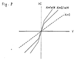
- I-V characteristic there are mainly two types of I-V characteristic: the Poole-Frenkcl characteristic and the switching characteristic.
- the switching characteristic indicates a high resistance state and a low resistance state.
- the Poole-Frenkcl characteristic is described in H. Murry, Thin Solid Films 22 (1974) 37, and the switching characteristic is described in Masahiro Fukuzawa, Applied Physics Vol. 46, No. 7 (1977).
- Figure 31 is a graph illustrating a curve representing the I-V characteristic of the ZnS film which indicates the switching characteristic.
- the resistance of the ZnS film drastically changes at a threshold level of the applied voltage V TH , and thus the curve representing the I-V characteristic is discontinuous.
- V O the threshold level of the applied voltage
- the I-V characteristic curve has different values of current I corresponding to the same value of voltage V between V O and V TH .
- the I-V characteristic of the ZnS around the threshold level of the applied voltage is extremely unstable and is not reliable. A film having such an I-V characteristic is not suitable for a display apparatus.
- continuous means that the curve has a continuous slope in which the inclination increases or decreases but does not change to the opposite direction.
- Figure 4 shows a curve representing the I-V characteristic of a ZnS film used in a display apparatus according to the present invention.
- a ZnS thin film which realizes an I-V characteristic showing a continuous curve is used, and therefore the I-V characteristic is stable even around the threshold level of the applied voltage.
- the I-V characteristic of the ZnS film is better in steepness than that of the insulation layer (active layer) formed of Ta2O5 or SiN x . This means that the ZnS film used in the present invention is suitable for the switching device.
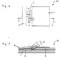
- Figures 1 and 2 show a part of an LCD apparatus 20 in the first example according to the present invention.
- Figure 1 is a top view of a rectangular pixel electrode 5 and a vicinity thereof in the LCD apparatus 20; and
- Figure 2 is a cross sectional view of the LCD apparatus 20 shown in Figure 1 looking along section line 2'-2' in Figure 1.
- the LCD apparatus 20 includes an insulating base substrate 1 formed of glass or the like.
- a plurality of pixel electrodes 5 (only one is shown in Figure 1) are arranged in a matrix on a top surface of the base substrate 1.
- a plurality of scanning lines 2 (only one is shown in Figure 1) respectively corresponding to the pixel electrodes 5 are also on the top surface of the base substrate 1, each for sending a timing signal to the corresponding pixel electrode 5 in order to drive the pixel electrode 5.
- Each pixel electrode 5 and the corresponding scanning line 2 are connected to each other by a switching element.
- a two-terminal device including a ZnS layer is used as the switching device. The continuous and steep I-V characteristic of the ZnS layer is used.
- a first electrode 4 is branched from the scanning line 2.
- the first electrode 4 includes a first section 6 extended perpendicularly to the scanning line 2 and a second section 7 extended perpendicularly to the first section 6.
- the second section 7 is parallel to the scanning line 2.
- a ZnS layer 3 formed of a thin ZnS film is on the entire top surface of the base substrate 1, covering the scanning line 2 and the first electrode 4.
- the pixel electrode 5 is on the ZnS layer 3 along the scanning line 2.
- a second electrode 8 is branched from the pixel electrode 5 in such a direction as to cross the second section 7 of the first electrode 4.
- the second electrode 8 partially covers the second section 7 of the first electrode 4 with the ZnS layer sandwiched therebetween.
- a two-terminal device 14 includes a three-layer structure including the first electrode 4, the ZnS layer 3 and the second electrode 8.
- An alignment film 9 is on the entire base substrate 1, covering the ZnS layer 3 and the pixel electrode 5.
- FIG 3 is a partial isometric view of the display apparatus 20 shown in Figures 1 and 2.
- an insulating counter substrate 12 formed of glass or the like is opposed to the base substrate 1 with a liquid crystal layer 10 as a display medium sandwiched therebetween.
- a plurality of counter electrodes 13 are on the bottom surface of the counter substrate 12 facing the bass substrate 1, the counter electrodes 13 being arranged in such a direction as to cross the scanning line 2.
- An alignment film 11 is on the entire bottom surface of the counter substrate 12, covering the counter electrodes 13.
- the LCD apparatus 20 having the above-described structure is produced in the following manner.
- a conductive thin film formed of Ta is formed in a specified thickness (300 nm in the first example) by sputtering.
- the conductive thin film may be formed by CVD, evaporation or the like instead of sputtering.
- the conductive thin film formed of Ta is patterned into a specified pattern so as to form the scanning line 2 having the first electrode 4.
- the ZnS layer 3 is formed on the entire top surface of the base substrate 1 in a specified thickness by sputtering so as to cover the scanning line 2 and the first electrode 4.
- the thickness of the ZnS layer 3 is determined as follows based on the driving voltage for the LCD apparatus 20. Namely, the voltage which is necessary to cause liquid crystal molecules in the liquid crystal layer 10 as the display medium to display an image.
- the threshold level of the electric field or withstand voltage
- the threshold voltage depends on the thickness of the ZnS layer 3. Accordingly, the thickness of the ZnS layer 3 is determined so that the voltage applied to the liquid crystal layer 10 will reach the driving voltage for display when the voltage applied to the ZnS layer 3 exceeds the threshold level. Namely, when the ZnS layer 3 as the switching device is turned "ON".
- the threshold level of the electric field is in proportion to the thickness of the ZnS layer 3. Where the thickness is less than 10 nm, the I-V characteristic is unstable; and where the thickness is more than 1 ⁇ m, the steepness of the I-V characteristic declines. Accordingly, in order to obtain a stable and steep I-V characteristic, the thickness of the ZnS layer 3 should be between 10 nm and 1 ⁇ m, preferably 30 nm to 200 nm inclusive.
- sputtering target a highly pure, sintered ZnS target is used. Or, highly pure ZnS powders which are densely spread all over a quartz glass plate may be used.
- the sputtering is performed using argon (Ar) as the sputtering gas, at the substrate temperature of 250°C, with the gas pressure of 10 Pa and the input power of 750 W.
- the ZnS layer 3 may be formed by CVD, evaporation or other thin film formation methods instead of sputtering.
- the thickness of the ZnS layer 3 is 100 nm.
- a conductive film for forming the pixel electrode 5 is formed on the ZnS layer 3.
- an ITO film is formed by sputtering as the conductive film since ITO is suitable for a transmission type LCD apparatus due to the transparency thereof.
- the ITO film may be formed by CVD, evaporation or the like instead of sputtering.
- the conductive film may be formed of metal such as Al, Ni, Ti, Ag, Cr, Cu and alloys thereof.
- the ITO film is patterned into a specified pattern in order to form the pixel electrode 5 and the second electrode 8 which is extended in such direction as to cross the second section 7 of the first electrode 4 of the scanning line 2.
- the alignment film 9 is formed on the entire base substrate 1.
- the material for the alignment film 9 containing, for example, polyimide is formed on the entire base substrate 1, and then the material is cured and aligned.
- an ITO film is formed and patterned so as to form a plurality of counter electrodes 13 corresponding to the plurality of pixel electrodes 5, respectively.
- the counter electrodes 13 are arranged substantially in parallel to one another.
- Each counter electrode 13 has a width sufficient to cover the corresponding pixel electrode 5.
- the alignment film 11 is formed on the entire bottom surface of the counter substrate 12.
- a material for the alignment film 11 is formed on the entire bottom surface of the counter substrate 12 so as to cover the counter electrodes 13. The material is cured and then aligned.
- the base substrate 1 having the scanning lines 2, the pixel electrodes 5 and the like on the top surface thereof and the counter substrate 12 having the counter electrodes 13 and the like on the bottom surface thereof are assembled with spacers (not shown) sandwiched therebetween so that the top surface of the base substrate 1 and the bottom surface of the counter substrate 12 face each other and so that the scanning lines 2 and the counter electrodes 13 are arranged in such directions as to cross each other.
- the liquid crystal is injected between the base substrate 1 and the counter substrate 12 to form the liquid crystal layer 10, and then the liquid crystal layer 10 is sealed.
- the LCD apparatus 20 produced in the above-described manner operates in the following way.
- Figure 4 is a graph illustrating the curve representing the I-V characteristic of a two-terminal device used in the present invention, for example, the two-terminal device 14.
- the current I is represented in logarithmic scale in Figure 4.
- Figure 5 is an equivalent circuit diagram corresponding to one pixel of an LCD apparatus including the two-terminal device, for example, the LCD apparatus 20.
- the two-terminal device 14 has a capacitance C D
- the liquid crystal layer has a capacitance C L
- the pixel is equivalent to a circuit including the capacitances C D and C L connected with each other in series between the first electrode 4 and the counter electrode 13.
- V L V ⁇ C D /(C L + C D )
- Equation (4) it is apparent from Equation (4) that, when C L >>C D , V D is approximately equal to V. Accordingly, the voltage V D at a sufficient level is applied to the two-terminal device 14. When the voltage V D applied to the two-terminal device 14 exceeds the threshold voltage V TH of the two-terminal device 14, the two-terminal device 14 is turned ON.
- the two-terminal device 14 When the voltage V D applied to the two-terminal device 14 is decreased to below the threshold voltage V TH of the two-terminal device 14, the two-terminal device 14 is turned OFF. Even when the two-terminal device 14 is OFF, the liquid crystal molecules are driven by the electric charge stored in the capacitance C L of the liquid crystal layer 10 when the two-terminal device 14 is ON.
- Figures 6 and 7 show a part of an LCD apparatus 30 in the second example according to the present invention.
- Figure 6 is a top view of a rectangular pixel electrode 5 and a vicinity thereof in the LCD apparatus 30; and
- Figure 7 is a cross sectional view of the LCD apparatus 30 shown in Figure 6 looking along section line 7'-7' in Figure 6.
- the structure of the LCD apparatus 30 in the second example is identical with the structure of the LCD apparatus 20 in the first example except that a second electrode 15 formed of metal is provided independently instead of being extended from the pixel electrode 5.
- the second electrode 15 is on the second section 7 of the first electrode 4 with the ZnS layer 3 sandwiched therebetween.
- the pixel electrode 5 is on the ZnS layer 3, covering an end portion of the second electrode 15.
- the two-terminal device 14 includes the three-layer structure including the first electrode 4, the ZnS layer 3 and the second electrode 15. Due to such a structure, the ZnS layer 3 and the second electrode 15 are electrically connected to each other.
- the process for producing the LCD apparatus 30 requires the step of forming the second electrode 15 in addition to the production process of the LCD apparatus 20 described in the first example.
- the second electrode 15 and the pixel electrode 5 are formed of different materials from each other, the materials for the second electrode 15 and the pixel electrode 5 can be chosen from a wider selection of materials than in the first example.
- the ZnS layer 3 is formed by sputtering using a different target from the target used in the first and the second examples.
- the target used in the third example is obtained by doping manganese (Mn) in the sintered ZnS target.
- the target may be obtained by mixing Mn in highly pure ZnS powders and then densely spreading the resultant mixture all over a quartz glass plate. In this manner, Mn is implanted into the ZnS layer 3.
- Implantation of Mn into the ZnS layer 3 improves the withstand voltage of the ZnS layer 3 and thus enhances the reliability of the two-terminal device 14. Except for the material for the sputtering target, the LCD apparatus in the third example is identical with the LCD apparatuses in the first and the second examples.
- Mn other materials may be used.
- copper rare earth elements such as terbium (Tb), samarium (Sm), europium (Eu), or oxides, fluorides, carbonates, phosphates, oxalates, chlorides, bromides, iodides, nitrates or other compounds of such rare earth elements may be used.
- ZnS powders By mixing powders of these elements or compounds with the ZnS powders, at least one of these elements or compounds is implanted into the ZnS layer 3. In this manner, the withstand voltage of the ZnS layer 3 is improved, and thus the reliability of the two-terminal device 14 is enhanced.
- the two-terminal device in the third example has an I-V characteristic excellent in steepness and symmetry.
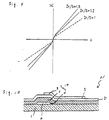
- the ZnS layer 3 is formed by sputtering using a different target from the target used in the previous three examples.
- the target used in the fourth example is obtained by doping Al in the sintered ZnS target.
- the target may be obtained by mixing Al powders in highly pure ZnS powdars and then densely spreading the resultant mixture all over a quartz glass plate. In this manner, Al is implanted into the ZnS layer 3.
- Figure 8 illustrates curves representing the I-V characteristic of the ZnS layers 3 including Al in various weight ratios. As is apparent from Figure 8, the I-V characteristic can be changed by the amount of Al included in the ZnS layer 3. As the amount of Al increases, the I-V characteristic increases in steepness.
- the LCD apparatus in the fourth example is identical with the LCD apparatuses in the previous three examples.
- III-group elements may be included in the ZnS layer 3 by implantation into the ZnS powders and the same effects can be obtained.
- the I-V characteristic of the ZnS layer 3 can easily be changed by varying the amount of Al or other III-group elements included in the ZnS layer 3. Utilizing this fact, a two-terminal device having an optimum I-V characteristic can be obtained in accordance with the electrooptic properties of the display medium used in an LCD apparatus to be produced.
- the ZnS layer 3 is formed by sputtering using a different target from the target used in the previous four examples.
- the target used in the fifth example is obtained by doping Zn in the sintered ZnS target. In this manner, the composition ratio of Zn and sulfur (S) in the ZnS layer 3 can be changed.
- Figure 9 illustrates curves representing the I-V characteristic of the ZnS layers 3 including Zn in various composition ratios with respect to S.
- the I-V characteristic can be changed by varying the composition ratio of Zn to S in the ZnS layer 3. As the composition ratio of Zn increases, the I-V characteristic increases in steepness.
- the LCD apparatus in the fifth example is identical with the LCD apparatuses in the previous four examples.
- the I-V characteristic of the ZnS layer 3 can easily be changed by varying the composition ratio of Zn to S included in the ZnS layer 3. Utilizing this fact, a two-terminal device-having an optimum I-V characteristic can be obtained in accordance with the electrooptic properties of the display medium used in an LCD apparatus to be produced.
- FIG 10 is a cross sectional view of an LCD apparatus 31 in the sixth example according to the present invention.
- an insulation layer 21 is sandwiched between the ZnS layer 3 (active layer) and the second electrode 4 of the pixel electrode 5.
- the insulation layer 21 is formed of SiN x by sputtering on the entire base substrate 1.
- the pixel electrode 5 having the second electrode 8 is formed on the insulation layer 21.
- the withstand voltage of the two-terminal device 14 is improved, and thus the reliability of the two-terminal device 14 is enhanced.
- the insulation layer 21 may be formed of any insulating material, preferably a nitrogen compound such as SiN x or AlN.
- the production process of the LCD apparatus 31 is identical with the production process described in the first example until the ZnS layer 3 is formed.
- the insulation layer 21 is formed on the entire ZnS layer 3 by sputtering, using silicon as a sputtering target under an atmosphere of a mixture gas of Ar and N2, at the substrate temperature of 250°C, the gas pressure of 8 Pa and the input power of 750 W.
- the pixel electrode 5 is formed on the insulation layer 21, the pixel electrode 5 is formed. After that, the production process of the LCD apparatus 31 is again identical with the process described in the first example.
- FIG 11 is a cross sectional view of an LCD apparatus 32 as a modification of the LCD apparatus 31.
- the insulation layer 21 is sandwiched between the first electrode 4 and the ZnS layer 3.
- FIG 12 is a cross sectional view of an LCD apparatus 33 as another modification of the LCD apparatus 31.
- an insulation layer 21 is sandwiched between the first electrode 4 and the ZnS layer 3, and another insulation layer 21 is sandwiched between the ZnS layer 3 and the second electrode 8.
- FIG. 13 is a graph illustrating the curve representing the Q-V characteristic of the two-terminal device 14 of the LCD apparatus 33. As is apparent from Figure 13, the Q-V characteristic is satisfactory both in steepness and symmetry.
- the insulation layer 21 may be formed of any insulating material.
- the two insulation layers 21 are preferably formed of an identical material in order to obtain a satisfactory Q-V characteristic.
- the insulation layer 21 may have a multiple layer structure instead of a single layer structure.
- the insulation layer 21 may have a two-layer structure of SiO2 and SiN x or have a three-layer structure of SiO2, Ta2O5 and SiN x .
- either one of the two insulation layers 21 sandwiching the ZnS layer 3 may include such a multiple layer structure.
- the two insulation layers 21 may both include a multiple layer structure.
- the ZnS layer 3 and the insulation layer 21 both transmit visible light. Therefore, there is no need to pattern the ZnS layer 3 and the insulation layer 21 to remove any part thereof corresponding to a display area (namely, an area except for the two-terminal device 14). Accordingly, the formation of the layers can be performed continuously by a thin film formation technology after the first electrode 4 is formed. Such continuous formation simplifies the production process and thus reduces the production cost.
- the ZnS layer 3 described in the first through sixth examples illustrated in, for example, Figures 2, 7 and 10 through 12 is heated.
- the heating temperature should be equal to or higher than the substrate temperature used for the formation of the ZnS layer 3.
- the heating is performed in a vacuum oven, in the temperature range of 300°C to 600°C inclusive for 1 hour. Instead of the vacuum oven, an ordinary oven or a sulfur atmosphere may be used.
- the ZnS layer 3 illustrated in Figures 2, 7 and 11 is heated before the formation of the pixel electrode 5 having the second electrode 8 or 15.
- the ZnS layer 3 may be heated after the formation of the pixel electrode 5 having the second electrode 8 or 15.
- the ZnS layer 3 illustrated in Figure 10 is heated before the insulation layer 21 is formed or after the pixel electrode 5 including the second electrode 8 is formed.
- the ZnS layer 3 illustrated in Figure 12 is heated before the formation of the insulation layer 21 on the ZnS layer 3 or after the formation of the pixel electrode 5 having the second electrode 8.
- the crystallinity of the ZnS layer 3 is improved. Further, the elements and the compounds described in the third, fourth and fifth examples are dispersed into the ZnS layer 3 by such heating when these elements and the compounds are implanted into the ZnS layer 3, and thus the ZnS layer 3 is made uniform in quality. Accordingly, the uniformity of characteristics and the reliability of the two-terminal device 14 are enhanced.
- An aging test of the two-terminal device 14 produced according to the production process described in the seventh example proves that the two-terminal device 14 in the seventh example has stable characteristics with less aging.
- An LCD apparatus including such a two-terminal device 14 has stable display characteristics.
- a two-terminal device 14 is produced in accordance with the production process described in the sixth example, and an LCD apparatus is also produced using such a two-terminal device 14.
- the insulation layer 21 is formed on the ZnS layer 3, and the pixel electrode 5 having the second electrode 8 is formed on the insulation layer 21.
- the pixel electrode 5 is formed of a transparent conductive material such as ITO, and the insulation layer 21 is formed of a nitrogen compound.
- heating the ZnS layer 3 improves the characteristics of the two-terminal device 14 as the switching device.
- the pixel electrode 5 is formed of ITO and the insulation layer 21 is formed of an oxide such as Ta2O5 or Y2O3, heating the ZnS layer 3 at a high temperature oxidizes a part of the pixel electrode 5 in contact with the insulation layer 21 and thus increases the surface resistance of the pixel electrode 5 formed of ITO.
- the insulation layer 21 is formed of a nitrogen compound in order to solve such an inconvenience.
- An LCD apparatus including such a two-terminal device 14 is produced in the same manner as that described in the first example.
- An aging test of the two-terminal device 14 formed in the eighth example proves that the two-terminal device 14 has stable characteristics with less aging as in the seventh example.
- the LCD apparatus including such a two-terminal device 14 also has stable display characteristics.
- Figure 14 is a cross sectional view of an LCD apparatus in a ninth example according to the present invention.
- an insulation layer 22 is sandwiched between the ZnS layer 3 and the pixel electrode 5 having the second electrode 8.
- the insulation layer 22 is formed by coating the ZnS layer 3 with a polymeric resin before forming the pixel electrode 5 having the second electrode 8.
- the insulation layer 22 also acts as a protection layer for the ZnS layer 3.
- the insulation layer 22 has a hole 23, and the hole 23 is filled with the second electrode 8.
- the ZnS layer 3 and the second electrode 8 are electrically connected with each other through the hole 23.
- the LCD apparatus 34 is identical in structure with the LCD apparatuses described in the first through the fifth examples.
- the LCD apparatus 34 shown in Figure 14 is produced in the following manner.
- the production process of the LCD apparatus 34 is identical with the production process described in the first example until the ZnS layer 3 is formed.
- the ZnS layer 3 is coated with a polymeric resin using a spinner, a roller coater or the like to form the insulation layer 23.
- the insulation layer 22 formed of a polymeric resin protects the ZnS layer 3 without influencing electric characteristics of the two-terminal device 14 of the LCD apparatus 34.
- Inorganic substances such as SiO2 or Al2O3 and organic substances such as acrylic resins, polyimide or polyurea may be used for a protection layer for the ZnS layer 3 instead of a polymeric resin.
- the hole 23 is formed in the insulation layer 22, at a portion thereof corresponding to the first electrode 4 by a photographic method. Then, the pixel electrode 5 having the second electrode 8 is formed in such a pattern that the second electrode 8 fills the hole 23. As is mentioned above, the ZnS layer 3 and the second electrode 8 (or the pixel electrode 5) are electrically connected with each other through the hole 23.
- Figure 16 is a schematic illustration of the process for forming the hole 23.
- the insulation layer 22 is formed on the ZnS layer 3 (part (a))
- the insulation layer 22 is coated with a negative photoresist 24, and the resultant lamination is exposed to light from the side of a bottom surface of the base substrate 1, using the first electrode 4 as a mask (part (b)).
- a part of the negative photoresist 24 shielded from the light by the first electrode 4 is removed by development and patterning (part (c)).
- a part of the insulation layer 22 corresponding to the first electrode 4 is removed in accordance with the pattern of the photoresist 24 to form the hole 23 (part (d)).
- the photoresist 24 is peeled off (part (e)), and the pixel electrode 5 having the second electrode 8 is formed on the insulation layer 22 to fill the hole 23 (part (f)).
- the pixel electrode 5 is electrically connected to the ZnS layer 3 through the hole 23.
- the insulation layer 22 is patterned to form the hole 23 in a self-alignment manner. Therefore, the hole 23 is formed at an appropriate position with no positional displacement.
- the production process is simple. As a result, a highly reliable two-terminal device 14 is produced with high efficiency.
- An aging test of the two-terminal device 14 produced in the ninth example proves that the two-terminal device 14 has stable characteristics with little aging as in the seventh and the eighth examples. This is due to the insulation layer 22 formed of a polymeric resin.
- the LCD apparatus 34 including such a two-terminal device 14 also has stable characteristics.
- the first electrode 4 is branched from the scanning line 2. Instead, a specified area within the scanning line 2 may be designated as the first electrode 4 as is illustrated in Figure 17. In such a case, the two-terminal device 14 is formed by laminating the ZnS layer 3 (active layer) and the second electrode 8 on the first electrode 4 at the specified area within the scanning line 2.
- FIG 15 is a cross sectional view of a modification of the LCD apparatus 34 in the ninth example.
- the insulation layer 21 formed of SiN x or the like is sandwiched between the second electrode 4 and the ZnS layer 3 in addition to the insulation layer 22.
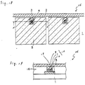
- Figure 18 is a top view of two pixels and the vicinity thereof in an LCD apparatus 36 in the tenth example; and Figure 19 is a cross sectional view of the LCD apparatus shown in Figure 18 looking across section line 19'-19' in Figure 18.
- the LCD apparatus 36 includes the base substrate 1.
- the scanning line 2 is on the top surface of the base substrate 1, and the first electrode 4 is branched from the scanning line 2.
- the ZnS layer 3 acting as an active layer is on a specified area of the first electrode 4. It should be noted that the ZnS layer 3 is not on the entire base substrate 1.
- an insulation layer 16 is on the base substrate 1, covering the first electrode 4 except for an the area on which the ZnS layer 3 is located.
- the insulation layer 16 has a greater thickness than that of the ZnS layer 3.
- the pixel electrode 5 is on the insulation layer 16, covering the ZnS layer 3.
- a part of the pixel electrode 5 which is on the ZnS layer 3 is the second electrode 8.
- the two-terminal device 14 includes the three-layer structure including the first electrode 4, the ZnS layer 3 and the second electrode 8.
- the LCD apparatus 36 having the above-described structure is produced in the following manner.
- Figure 20 is a schematic illustration of a part of the process for producing the LCD apparatus 36.
- a film of Ta is formed on the base substrate 1 in a specified thickness by sputtering and patterned into a specified pattern to form the scanning line 2 having the first electrode 4 (part (a)).
- the thickness of the scanning line 2 is 300 nm in the tenth example.
- the scanning line 2 having the first electrode 4 may be formed of a conductive thin film of titanium, molybdenum, aluminum, copper, ITO or the like instead of Ta.
- a mixed solution of hydrofluoric acid and nitric acid is used as an etchant for patterning.
- the insulation layer 16 is formed as is illustrated in parts (b) through (d).
- a film of SiO x is formed on the base substrate 1 to cover the first electrode 4 in a thickness of 1.0 ⁇ m (part (b)). Then, the film of SiO x is patterned into a specified pattern using a photoresist 17 and a mask 18 (parts (c) and (d)). In this way, the insulation layer 16 having a hole 19 at a portion corresponding to the two-terminal device 14 is formed.
- a photoresist 17 a positive photoresist OFPR-800 produced by Tokyo Ohka Kabushiki Kaisha is used in the tenth example, but a negative photoresist may be used.
- the patterning after development is performed by dry etching.
- the insulation layer 16 may be formed of an insulating material such as SiN x , Al2O3, or AlN instead of SiO x .
- the ZnS layer 3 is formed on the photoresist 17 to cover the first electrode 4 by sputtering in a thickness of 200 nm (part (e)).
- the photoresist 17 and the Zns layer 3 on the photoresist 17 are peeled off by a lift-off method (part (f)) to keep the ZnS layer 3 only on the first electrode 4 in the hole 19.
- a lift-off method part (f)
- OMR-710 produced by Tokyo Ohka Kabushiki Kaisha is used.
- a film of ITO is formed on the insulation layer 16 to cover the ZnS layer 3 to a thickness of 200 nm, and patterned to form the pixel electrode 5 having the second electrode 8 (part (g)).
- the pixel electrode 5 having the second electrode 8 may be formed of a conductive material such as aluminum, tantalum, titanium, molybdenum or copper instead of ITO.
- the two-terminal device 14 produced in the above-described manner includes a flat portion of the first electrode 4 but excludes a side portion and the vicinity thereof including an edge formed at the junction of a top surface 28 and a side surface 29 of the first electrode 4 and another edge formed at the junction of the side surface 29 and the interface between the first electrode 4 and the base substrate 1. Accordingly, insulation breakdown caused by insufficient insulation of the side portion of the first electrode 4 and the vicinity thereof by the insulation layer 16 does not influence the performance of the two-terminal device 14, and therefore a desirable I-V characteristic is obtained.
- the ZnS layer 3 is formed only in the hole 19, namely, in the area of the two-terminal device 14, the inconveniences such as increase in the leak current and fluctuation in impedance in accordance with the change in the applied voltage caused by the ZnS layer 3 on the area other than the two-terminal device 14 can be avoided.
- the insulation layer 16 covers the entire top surface of the base substrate 1, the flatness of the base substrate 1 is improved. Such improved flatness allows the liquid crystal molecules in the LCD apparatus 36 to be easily aligned. In the case that the two-terminal device 14 is used in a reflection type LCD apparatus, the light scattering characteristic of the LCD apparatus 36 is enhanced.
- Figure 21 is a schematic illustration of a part of a process for producing the LCD apparatus 36 for solving the problem of insufficient insulation of the first electrode 4 by the ZnS layer 3.
- a film of Ta is formed on the base substrate 1 in a specified thickness by sputtering and patterned into a specified pattern to form the scanning line 2 having the first electrode 4 (part (a)).
- the thickness of the scanning line 2 is 300 nm in the eleventh example.
- the scanning line 2 having the first electrode 4 may be formed of a conductive thin film of titanium, molybdenum, aluminum, copper, ITO or the like instead of Ta.
- a mixed solution of hydrofluoric acid and nitric acid is used as an etchant for patterning.
- the ZnS layer 3 is formed on the base substrate 1 to cover the first electrode 2 by sputtering in a thickness of 200 nm (part (b)). Then, the ZnS layer 3 is patterned into a specified pattern using the photoresist 17 and the mask 18 (parts (c) and (d)). Namely, a part of the photoresist 17 and a part of the ZnS layer 3 exposed to light are removed.
- the photoresist 17 a positive photoresist OFPR-800 produced by Tokyo Ohka Kabushiki Kaisha is used in the eleventh example, but a negative photoresist may be used.
- hydrochloric acid is used as an etchant for patterning the ZnS layer 3 after development.
- the insulation layer 16 is formed on the base substrate 1 to cover the photoresist 17 by sputtering in a thickness of 1.0 ⁇ m, the ZnS layer 3 and the first electrode 4 (part (e)).
- the insulation layer 16 may be formed of an insulating material such as SiN x or a photoresist.
- the photoresist 17 and the SiO x layer on the photoresist 17 are peeled off by a lift-off method (part (f)) to form the insulation layer 16 having the hole 19 at a portion corresponding to the ZnS layer 3.
- the insulation layer 16 covers the base substrate 1 and the first electrode 4 except for an area on which the ZnS layer 3 is located. In other words, the ZnS layer 3 is only in the hole 19 of the insulation layer 16, namely, in the area of the two-terminal device 14.
- As the peeling-off liquid OMR-710 produced by Tokyo Ohka Kabushiki Kaisha is used.
- a film of ITO is formed on the insulation layer 16 to cover the ZnS layer 3 by sputtering to a thickness of 200 nm, and patterned to form the pixel electrode 5 having the second electrode 8 (part (g)).
- the pixel electrode 5 having the second electrode 8 may be formed of a conductive material such as aluminum, tantalum, titanium, molybdenum or copper instead of ITO.
- As an etchant for patterning the ITO film hydrobromic acid is used.
- the two-terminal device 14 produced in the above-described manner includes a flat portion of the first electrode 4 but excludes a side portion and the vicinity thereof including an edge formed at the junction of a top surface 28 and a side surface 29 of the first electrode 4 and another edge formed at the junction of the side surface 29 and the interface between the first electrode 4 and the base substrate 1. Accordingly, insulation breakdown caused by insufficient insulation of the side portion of the first electrode 4 and the vicinity thereof by the insulation layer 16 does not influence the performance of the two-terminal device 14, and therefore a desirable I-V characteristic is obtained.
- the ZnS layer 3 is formed only in the hole 19, namely, in the area of the two-terminal device 14, the inconveniences such as increases in the leak current and fluctuations in impedance in accordance with the change in the applied voltage caused by the ZnS layer 3 formed on the area other than the two-terminal device 14 can be avoided.
- the insulation layer 6 covers the entire top surface of the base substrate 1, the flatness of the base substrate 1 is improved. Such improved flatness allows the liquid crystal molecules in the LCD apparatus 36 to be easily aligned. In the case that the two-terminal device 14 is used in a reflection type LCD apparatus, the light scattering characteristic of the LCD apparatus 36 is enhanced.
- Figure 22 is a partial cross sectional view of an LCD apparatus 37 in the twelfth example.
- the LCD apparatus 37 includes the base substrate 1.
- the scanning line 2 is on the top surface of the base substrate 1, and the first electrode 4 is branched from the scanning line 2.
- the ZnS layer 3 acting as an active layer is on a specified area of the first electrode 4. It should be noted that the ZnS layer 3 is not on the entire base substrate 1.
- the insulation layer 16 is on the base substrate 1, covering the first electrode 4 except for an area on which the ZnS layer 3 is located.
- the insulation layer 16 has a greater thickness than that of the ZnS layer 3.
- a second electrode 25 formed of a conductive thin film is on the ZnS layer 3.
- the pixel electrode 5 is on the insulation layer 16, covering the second electrode 25.
- the two-terminal device 14 includes the three-layer structure including the first electrode 4, the ZnS layer 3 and the second electrode 25.
- the LCD apparatus 37 having the above-described structure is produced in the following manner.
- Figure 23 is a schematic illustration of a part of the process for producing the LCD apparatus 37.
- a film of Ta is formed on the base substrate 1 in a specified thickness by sputtering and patterned into a specified pattern so as to form the scanning line 2 having the first electrode 4 (part (a)).
- the thickness of the scanning line 2 is 300 nm in the twelfth example.
- the scanning line 2 having the first electrode 4 may be formed of a conductive thin film of titanium, molybdenum, aluminum, copper, ITO or the like instead of Ta.
- a mixed solution of hydrofluoric acid and nitric acid is used as an etchant for patterning.
- the insulation layer 16 is formed as is illustrated in parts (b) through (d).
- a film of SiO x is formed on the base substrate 1 to cover the first electrode 4 in a thickness of 1.0 ⁇ m (part (b)). Then, the film of SiO x is patterned into a specified pattern using a photoresist 17 and a mask 18 (parts (c) and (d)). In this way, the insulation layer 16 having the hole 19 at the portion corresponding to the two-terminal device 14 is formed.
- a photoresist 17 a positive photoresist OFPR-800 produced by Tokyo Ohka Kabushiki Kaisha is used in the tenth example, but a negative photoresist may be used.
- the patterning after development is performed by dry etching.
- the insulation layer 16 may be formed of an insulating material such as SiN x , Al2O3, or AlN instead of SiO x .
- the ZnS layer 3 is formed on the photoresist 17 to cover the first electrode 4 by sputtering in a thickness of 200 nm (part (e)).
- a conductive thin film for forming the second electrode 25 is formed on the ZnS layer 3 by sputtering to a thickness of 800 nm (part (f)).
- titanium is used for the conductive thin film.
- aluminum, ITO, tantalum, molybdenum, copper or the like may be used.
- the photoresist 17, and a part of the ZnS layer 3 and a part of the conductive film both corresponding to the photoresist 17 are peeled off by a lift-off method to keep the ZnS layer 3 only in the hole 19 and also to form the second electrode 25 only in the hole 19 (part (g)).
- the ZnS layer 3 and the second electrode 3 are formed only in the area of the two-terminal device 14.
- OMR-710 produced by Tokyo Ohka Kabushiki Kaisha is used.
- a film of ITO is formed on the insulation layer 16 to cover the second electrode 25 by sputtering to a thickness of 200 nm and patterned to form the pixel electrode 5 (part (h)).
- the pixel electrode 5 may be formed of a conductive material such as aluminum, tantalum, titanium, molybdenum or copper instead of ITO.
- a mixed solution of hydrofluoric acid and nitric acid is used as an etchant for patterning the ITO film.
- the process for producing the LCD apparatus 37 requires the step of forming the second electrode 25 in addition to the production process of the LCD apparatus 36 described in the tenth and the eleventh examples.
- the second electrode 25 and the pixel electrode 5 are formed of different materials from each other, the materials for the second electrode 25 and the pixel electrode 5 can be chosen from a wider selection of materials than in the tenth and the eleventh examples.
- Figure 24 is a schematic illustration of a part of a process for producing the LCD apparatus 37 for solving the problem of insufficient insulation of the first electrode 4 by the ZnS layer 3.
- a film of Ta is formed on the base substrate 1 in a specified thickness by sputtering and patterned into a specified pattern to form the scanning line 2 having the first electrode 4 (part (a)).
- the thickness of the scanning line 2 is 300 nm in the thirteenth example.
- the scanning line 2 having the first electrode 4 may be formed of a conductive thin film of titanium, molybdenum, aluminum, copper, ITO or the like instead of Ta.
- a mixed solution of hydrofluoric acid and nitric acid is used as an etchant for patterning.
- the ZnS layer 3 is formed on the base substrate 1 to cover the first electrode 2 by sputtering in a thickness of 200 nm (part (b)). Then, a conductive thin film for forming the second electrode 25 is formed on the ZnS layer 3 by sputtering to a thickness of 800 nm (part (c)).
- the conductive thin film is formed of titanium. Instead of titanium, aluminum, ITO, tantalum, molybdenum, copper or the like may be used for the conductive thin film.
- the ZnS layer 3 and the titanium film are patterned into a specified pattern using the photoresist 17 and the mask 18 (parts (d) and (e)). Namely, a part of the photoresist 17, a part of the ZnS layer 3 and a part of the titanium film exposed to light are removed. In this manner the titanium film is patterned to be the second electrode 25.
- a positive photoresist OFPR-800 produced by Tokyo Ohka Kabushiki Kaisha is used in the eleventh example, but a negative photoresist may be used.
- etchant for patterning the titanium film after development a mixture liquid of an aqueous solution of hydrogen peroxide and an aqueous solution of ammonia is used.
- hydrochloric acid is used as an etchant for patterning the ZnS layer 3 after development.
- the insulation layer 16 is formed of an insulating material such as SiN x or a photoresist.
- the photoresist 17 and the SiO x film on the photoresist 17 are peeled off by a lift-off method (part (g)) to form the insulation layer 16 enclosing the ZnS layer 3 and the second electrode 25.
- the insulation layer 16 covers the base substrate 1 and the first electrode 4 except for an area on which the ZnS layer, 3 and the second electrode 25 are located. In other words, the ZnS layer 3 is only in the area of the two-terminal device 14.
- As for the peeling-off liquid OMR-710 produced by Tokyo Ohka Kabushiki Kaisha is used.
- a film of ITO is formed on the insulation layer 16 to cover the second electrode 25 by sputtering to a thickness of 200 nm, and patterned to form the pixel electrode 5 (part (h)).
- the pixel electrode 5 may be formed of a conductive material such as aluminum, tantalum, titanium, molybdenum or copper instead of ITO.
- As an etchant for patterning the ITO film hydrobromic acid is used.
- the process for producing the LCD apparatus 37 requires the step of forming the second electrode 25 in addition to the production process of the LCD apparatus 36 described in the tenth and the eleventh examples.
- the second electrode 25 and the pixel electrode 5 are formed of different materials from each other, the materials for the second electrode 25 and the pixel electrode 5 can be chosen from a wider selection of materials than in the tenth and the eleventh examples.
- Figure 25 is a partial cross sectional view of an LCD apparatus 38 in the fourteenth example according to the present invention.
- the LCD apparatus 38 is produced in the following manner.
- the production process of the LCD apparatus 38 is identical as the production process described in the first example until the ZnS layer 3 is formed.
- an insulation layer 26 is formed of a photosensitive resin.
- an inorganic oxide such as SiO2 or Al2O5
- an inorganic nitride such as SiN x or AlN
- an organic substance such as acrylic resins, polyimide, or polyurea
- a hole 27 is formed in the insulation layer 26, at a portion corresponding to the two-terminal device 14. A part of a surface of the insulation layer 26 corresponding to the pixel is corrugated by a photographic process.
- a conductive film is formed on the insulation layer 26 and patterned into a specified pattern to form the pixel electrode 5 having the second electrode 8.
- the pixel electrode 5 may be formed of Al, Ag, Cr, Ni, Cu, Ti or alloys thereof.
- a top part of the hole 27 has an area of 10 ⁇ m2 to 1,000 ⁇ m2 inclusive.
- the capacitance of the two-terminal device 14 is too large, and thus the ratio of the capacitance of the liquid crystal layer 10 with respect to the capacitance of the two-terminal device 14 (C L /C D ) is too small. Accordingly, the two-terminal device 14 is not supplied with a voltage at a sufficient level and is not conductive. As a result, the liquid crystal layer 10 is not supplied with a voltage at a sufficient level.
- the ratio of the capacitance of the liquid crystal layer 10 with respect to the capacitance of the two-terminal device 14 (C L /C D ) is sufficiently large.
- the amount of the current flowing through the liquid crystal layer 10 is too small, and thus the liquid crystal layer 10 is not sufficiently charged. For these reasons, it is important to choose an appropriate area of the top part of the hole 27.
- a material for the alignment film 9 is formed to cover the insulation layer 26 and the pixel electrode 5.
- the material is then cured and aligned to form the alignment film 9. In this manner, the lamination on the base substrate 1 is completed.
- counter electrodes 13 are formed in stripes in such a direction as to cross the pixel electrode 5.
- a material for the alignment film 11 is formed on the counter substrate 12 to cover the counter electrodes 13. The material is then cured and aligned to form the alignment film 11. In this manner, the lamination on the counter substrate 12 is completed.
- the lamination on the base substrate 1 and the lamination on the counter substrate 12 are assembled together with spacers (not shown) sandwiched therebetween, and the liquid crystal is injected between the two laminations to form the liquid crystal layer 10.
- the LCD apparatus 38 is produced.
- White-Taylor guest-host liquid crystal is used.
- the pixel electrode 5 is formed of metal in order to be suitable for a reflection type LCD apparatus. Since the surface of the insulation layer 26 is corrugated, a surface of the pixel electrode 5 formed on the insulation layer 26 is also corrugated. By such corrugation, the light incident on the LCD apparatus 38 is not reflected in such a manner as is reflected on a mirror surface, and thus the display quality is enhanced.
- the White-Taylor guest host liquid crystal does not require a deflection plate, and therefore displays brighter images than the conventional twisted nematic liquid crystal when used in a reflection-type LCD apparatus. Even in a transmission type LCD apparatus, the White-Taylor guest host liquid crystal displays brighter images than the conventional twisted nematic liquid crystal.
- the White-Taylor liquid crystal requires a high driving voltage. Accordingly, satisfactory displays cannot be obtained in an LCD apparatus including the conventional two-terminal device using Ta2O5 or SiN x in the case that the White-Taylor liquid crystal is used as the display medium. By using a two-terminal device using ZnS according to the present invention, satisfactory display is obtained even if the White-Taylor liquid crystal is used as the display medium.
- the insulation layer 26 of the LCD apparatus 38 is formed of an insulating color photoresist. Except for the material of the insulation layer 26, the LCD apparatus 38 is identical in structure with the LCD apparatus in the fourteenth example.
- the color photoresist for example, the Color Mosaic CK produced by Fuji Hunt Electronics Technology Kabushiki Kaisha is used.
- the LCD apparatus 38 in the fifteenth example is produced in the following manner.
- the ZnS layer 3 is formed in the manner described in the first example, a layer of the color photoresist is formed on the ZnS layer 3 to a thickness of approximately 300 nm by a spinner. Then, the hole 27 is formed in the insulation layer 26 and the surface of the insulation layer 26 is corrugated in the manner described in the fourteenth example. After that, the production process of the LCD apparatus 38 in the fifteenth example is also identical with the production process described in the fourteenth example.
- the insulation layer 26 Due to the color photoresist used for the insulation layer 26, the light incident on an area other than the pixel is absorbed by the insulation layer 26. In other words, the insulation layer 26 acts as a black matrix, and thus the display contrast is improved.
- the two-terminal device of the LCD apparatus includes an insulation layer (active layer) formed of ZnS, which has an I-V characteristic showing a continuous curve. Accordingly, a two-terminal having an I-V characteristic which is satisfactory both in steepness and symmetry and is excellent in nonlinearity can be obtained.
- a display apparatus including such a two-terminal device realizes high quality display.
- a display apparatus including such a two-terminal device has few defects in images and little dispersion in display quality among the pixels.
- the ZnS layer is formed only on a flat portion of the surface of the first electrode. Accordingly, the side portion of the first electrode and the vicinity thereof including the edges of the first electrode is excluded from the two-terminal device. Due to such a structure, the problem caused in, for example, a conventional MIM element, namely, insulation breakdown caused by insufficient insulation of the side portion of the first metal layer and the vicinity thereof is solved.
- the ZnS layer is formed only in the area of the two-terminal device, increase in the leak current and fluctuation in impedance in accordance with the change in the applied voltage which are caused by the ZnS layer formed in an area other than the two-terminal device is avoided.
- the I-V characteristic of the two-terminal device can easily be changed. Utilizing this fact, a two-terminal device having an optimum I-V characteristic in accordance with the display medium, the purpose for display, or the type of the display apparatus to be produced can be obtained.
Landscapes
- Physics & Mathematics (AREA)
- Nonlinear Science (AREA)
- Liquid Crystal (AREA)
- Engineering & Computer Science (AREA)
- Microelectronics & Electronic Packaging (AREA)
- Mathematical Physics (AREA)
- Chemical & Material Sciences (AREA)
- Crystallography & Structural Chemistry (AREA)
- General Physics & Mathematics (AREA)
- Optics & Photonics (AREA)
Applications Claiming Priority (6)
| Application Number | Priority Date | Filing Date | Title |
|---|---|---|---|
| JP16568/93 | 1993-02-03 | ||
| JP1656893 | 1993-02-03 | ||
| JP23057993 | 1993-09-16 | ||
| JP230579/93 | 1993-09-16 | ||
| JP31562093A JP3051627B2 (ja) | 1993-02-03 | 1993-12-15 | 表示装置およびその製造方法 |
| JP315620/93 | 1993-12-15 |
Publications (2)
| Publication Number | Publication Date |
|---|---|
| EP0610083A1 true EP0610083A1 (de) | 1994-08-10 |
| EP0610083B1 EP0610083B1 (de) | 1997-09-10 |
Family
ID=27281463
Family Applications (1)
| Application Number | Title | Priority Date | Filing Date |
|---|---|---|---|
| EP94300809A Expired - Lifetime EP0610083B1 (de) | 1993-02-03 | 1994-02-03 | Anzeigegerät mit einem zweipoligen, eine Zinksulfidschicht enthaltenden Bauteil und Verfahren zu seiner Herstellung |
Country Status (4)
| Country | Link |
|---|---|
| US (2) | US5642212A (de) |
| EP (1) | EP0610083B1 (de) |
| JP (1) | JP3051627B2 (de) |
| DE (1) | DE69405419T2 (de) |
Cited By (1)
| Publication number | Priority date | Publication date | Assignee | Title |
|---|---|---|---|---|
| EP0786151A4 (de) * | 1994-10-14 | 1999-08-11 | Energy Conversion Devices Inc | Flüssigkristall-anzeigevorrichtung mit einem schwellwertschalter |
Families Citing this family (14)
| Publication number | Priority date | Publication date | Assignee | Title |
|---|---|---|---|---|
| JP2912176B2 (ja) * | 1994-12-28 | 1999-06-28 | 日本電気株式会社 | 反射型液晶表示装置 |
| JPH09146123A (ja) * | 1995-11-16 | 1997-06-06 | Sharp Corp | 2端子非線形素子及びその製造方法 |
| JPH1054995A (ja) * | 1996-06-06 | 1998-02-24 | Pioneer Electron Corp | 反射型液晶表示装置 |
| JPH1022546A (ja) * | 1996-07-08 | 1998-01-23 | Sharp Corp | 非線形素子 |
| KR20000004422A (ko) | 1998-06-30 | 2000-01-25 | 김영환 | 고개구율 액정표시소자의 화소전극 형성방법 |
| JP2002162646A (ja) * | 2000-09-14 | 2002-06-07 | Sony Corp | 反射型液晶表示装置 |
| US7190008B2 (en) | 2002-04-24 | 2007-03-13 | E Ink Corporation | Electro-optic displays, and components for use therein |
| JP2004241397A (ja) * | 2003-01-23 | 2004-08-26 | Dainippon Printing Co Ltd | 薄膜トランジスタおよびその製造方法 |
| KR100558985B1 (ko) * | 2003-06-27 | 2006-03-10 | 엘지.필립스 엘시디 주식회사 | 액정 표시 장치용 어레이 기판의 제조 방법 |
| JP2007511786A (ja) * | 2003-10-27 | 2007-05-10 | イー インク コーポレイション | 電気光学ディスプレイ |
| KR100566816B1 (ko) * | 2003-11-04 | 2006-04-03 | 엘지.필립스 엘시디 주식회사 | 수평 전계 인가형 박막 트랜지스터 기판 및 그 제조 방법 |
| TWI336792B (en) * | 2006-04-07 | 2011-02-01 | Au Optronics Corp | Manufacturing method for a bottom substrate of a liquid crystal display device |
| JP2016112279A (ja) * | 2014-12-17 | 2016-06-23 | セイコーエプソン株式会社 | 画像取得装置、生体情報取得装置、電子機器 |
| CN113013329B (zh) * | 2021-02-22 | 2022-07-05 | 华中科技大学 | 一种透明的自选色的异质结忆阻器及其制备方法 |
Citations (3)
| Publication number | Priority date | Publication date | Assignee | Title |
|---|---|---|---|---|
| JPS5646584A (en) * | 1979-09-26 | 1981-04-27 | Hitachi Ltd | Multilayer thin film functional element and manufacture thereof |
| JPH01270027A (ja) * | 1988-04-22 | 1989-10-27 | Seiko Epson Corp | 液晶表示装置 |
| EP0464810A2 (de) * | 1990-07-06 | 1992-01-08 | Seiko Epson Corporation | Verfahren zur Herstellung eines Substrates für eine Flüssigkristall-Anzeigevorrichtung |
Family Cites Families (22)
| Publication number | Priority date | Publication date | Assignee | Title |
|---|---|---|---|---|
| US3732429A (en) * | 1971-11-12 | 1973-05-08 | Hughes Aircraft Co | Liquid crystal device |
| JPS4975096A (de) * | 1972-11-21 | 1974-07-19 | ||
| US4413883A (en) * | 1979-05-31 | 1983-11-08 | Northern Telecom Limited | Displays controlled by MIM switches of small capacitance |
| JPS6132674A (ja) * | 1984-07-25 | 1986-02-15 | Sony Corp | スチル画記録装置 |
| JPS6132673A (ja) * | 1984-07-25 | 1986-02-15 | Hitachi Ltd | テレビジヨン受信機 |
| US4775549A (en) * | 1984-12-19 | 1988-10-04 | Matsushita Electric Industrial Co., Ltd. | Method of producing a substrate structure for a large size display panel and an apparatus for producing the substrate structure |
| JPH0616506B2 (ja) * | 1984-12-26 | 1994-03-02 | 株式会社半導体エネルギー研究所 | 積層体の側周辺に選択的に被膜を形成する方法 |
| US4730903A (en) * | 1985-01-23 | 1988-03-15 | Semiconductor Energy Laboratory Co., Ltd. | Ferroelectric crystal display panel and manufacturing method thereof |
| JPS626221A (ja) * | 1985-07-02 | 1987-01-13 | Matsushita Electric Ind Co Ltd | 液晶セル |
| JPS6211828A (ja) * | 1986-03-14 | 1987-01-20 | Seiko Epson Corp | 液晶表示装置 |
| US5105289A (en) * | 1988-07-14 | 1992-04-14 | Seiko Epson Corporation | Reflection type electrooptical device and a projection type display apparatus using the same |
| NL8900521A (nl) * | 1989-03-03 | 1990-10-01 | Philips Nv | Schakeleenheid ten behoeve van een weergeefinrichting en weergeefinrichting voorzien van een dergelijke schakeleenheid. |
| US5019530A (en) * | 1990-04-20 | 1991-05-28 | International Business Machines Corporation | Method of making metal-insulator-metal junction structures with adjustable barrier heights |
| US5124822A (en) * | 1990-05-08 | 1992-06-23 | Raychem Corporation | Varistor driven liquid crystal display |
| JPH04318785A (ja) * | 1991-04-18 | 1992-11-10 | Matsushita Electric Ind Co Ltd | 映像信号の圧縮符号化処理方法及びその装置 |
| JPH0512688A (ja) * | 1991-07-08 | 1993-01-22 | Matsushita Electric Ind Co Ltd | 情報記録再生装置 |
| JPH0572567A (ja) * | 1991-09-13 | 1993-03-26 | Toppan Printing Co Ltd | 液晶表示装置の製造方法 |
| JPH0572570A (ja) * | 1991-09-18 | 1993-03-26 | Ricoh Co Ltd | 液晶表示装置及びその製造方法 |
| JPH0643497A (ja) * | 1992-07-24 | 1994-02-18 | Sharp Corp | 液晶表示装置 |
| US5464990A (en) * | 1992-09-25 | 1995-11-07 | Fuji Xerox Co., Ltd. | Voltage non-linear device and liquid crystal display device incorporating same |
| JPH06313899A (ja) * | 1993-04-30 | 1994-11-08 | Sharp Corp | 液晶表示装置 |
| JPH07152049A (ja) * | 1993-11-29 | 1995-06-16 | Sharp Corp | 液晶表示装置およびその製造方法 |
-
1993
- 1993-12-15 JP JP31562093A patent/JP3051627B2/ja not_active Expired - Fee Related
-
1994
- 1994-02-02 US US08/191,198 patent/US5642212A/en not_active Expired - Fee Related
- 1994-02-03 EP EP94300809A patent/EP0610083B1/de not_active Expired - Lifetime
- 1994-02-03 DE DE69405419T patent/DE69405419T2/de not_active Expired - Fee Related
-
1995
- 1995-05-30 US US08/453,360 patent/US5663020A/en not_active Expired - Fee Related
Patent Citations (3)
| Publication number | Priority date | Publication date | Assignee | Title |
|---|---|---|---|---|
| JPS5646584A (en) * | 1979-09-26 | 1981-04-27 | Hitachi Ltd | Multilayer thin film functional element and manufacture thereof |
| JPH01270027A (ja) * | 1988-04-22 | 1989-10-27 | Seiko Epson Corp | 液晶表示装置 |
| EP0464810A2 (de) * | 1990-07-06 | 1992-01-08 | Seiko Epson Corporation | Verfahren zur Herstellung eines Substrates für eine Flüssigkristall-Anzeigevorrichtung |
Non-Patent Citations (5)
| Title |
|---|
| BARAFF ET AL.: "THE OPTIMIZATION OF METAL-INSULATOR-METAL NONLINEAR DEVICES FOR USE IN MULTIPLEXED LIQUID CRYSTAL DISPLAYS", IEEE TRANSACTIONS ON ELECTRON DEVICES, vol. ED-28, no. 6, June 1981 (1981-06-01), pages 736 - 739, XP000615687 * |
| DATABASE WPI Section Ch Week 8124, Derwent World Patents Index; Class L03, AN 81-43253 * |
| H. MURRAY ET AL.: "CONDUCTION IN THIN FILMS OF R.F. REACTIVELY SPUTTERED ZINC SULPHIDE", THIN SOLID FILMS, vol. 22, 1974, pages 37 - 44, XP025703192, DOI: doi:10.1016/0040-6090(74)90277-6 * |
| PATENT ABSTRACTS OF JAPAN vol. 14, no. 31 (P - 993) 22 January 1990 (1990-01-22) * |
| R. R. SUTHERLAND: "A THEORY FOR NEGATIVE RESISTANCE AND MEMORY EFFECTS IN THIN INSULATING FILMS AND ITS APPLICATION TO AU-ZNS-AU DEVICES", J . PHYS. D: APPL. PHYS., vol. 4, 1971, GREAT BRITAIN, pages 468 - 479, XP001628730 * |
Cited By (1)
| Publication number | Priority date | Publication date | Assignee | Title |
|---|---|---|---|---|
| EP0786151A4 (de) * | 1994-10-14 | 1999-08-11 | Energy Conversion Devices Inc | Flüssigkristall-anzeigevorrichtung mit einem schwellwertschalter |
Also Published As
| Publication number | Publication date |
|---|---|
| JPH07134315A (ja) | 1995-05-23 |
| US5642212A (en) | 1997-06-24 |
| EP0610083B1 (de) | 1997-09-10 |
| DE69405419T2 (de) | 1998-03-19 |
| JP3051627B2 (ja) | 2000-06-12 |
| US5663020A (en) | 1997-09-02 |
| DE69405419D1 (de) | 1997-10-16 |
Similar Documents
| Publication | Publication Date | Title |
|---|---|---|
| EP0610083B1 (de) | Anzeigegerät mit einem zweipoligen, eine Zinksulfidschicht enthaltenden Bauteil und Verfahren zu seiner Herstellung | |
| EP0202092B1 (de) | Flüssigkristallanzeigevorrichtung | |
| US7768011B2 (en) | Electro-luminescence device including a thin film transistor and method of fabricating an electro-luminescence device | |
| EP0622659B1 (de) | Flüssigkristall-Anzeigevorrichtung mit einem Zweipolelement als Schalteinrichtung | |
| GB2091468A (en) | Matrix liquid crystal display device and method of manufacturing the same | |
| US4653858A (en) | Method of fabrication of diode-type control matrices for a flat electrooptical display screen and a flat screen constructed in accordance with said method | |
| EP0385419A1 (de) | Flüssigkristall-Anzeigevorrichtung | |
| US5552910A (en) | Liquid crystal display having zinc sulfide switching elements and method for producing the same | |
| US4810637A (en) | Non-linear control element for a flat electrooptical display screen and a method of fabrication of said control element | |
| EP0182484B2 (de) | Flüssigkristallanzeigevorrichtung | |
| US5734452A (en) | Two-terminal non-linear resistive device and a method for producing the same in which nickel or iron is an impurity in the zinc sulfide layer | |
| JPH0230019B2 (de) | ||
| US6271050B1 (en) | Method of manufacturing thin film diode | |
| KR100247110B1 (ko) | 전기 광학 장치 | |
| CA2058902C (en) | Liquid crystal display | |
| EP0407164B1 (de) | Flüssigkristall-Anzeigevorrichtung | |
| EP0636922A1 (de) | Nichtlineares wiederstandselement, verfahren zu seiner herstellung und fluessigkristall-anzeigevorrichtung | |
| JPH0230020B2 (de) | ||
| JP3096372B2 (ja) | 2端子表示装置 | |
| EP0306338A1 (de) | Elektrooptische Vorrichtung | |
| JPH1022546A (ja) | 非線形素子 | |
| EP0333392A2 (de) | Elektrooptische Vorrichtung | |
| JP3052361B2 (ja) | アクティブマトリクス液晶表示装置とその製造方法 | |
| JP3054038B2 (ja) | 表示装置 | |
| JP3097948B2 (ja) | 非線形素子の製造方法 |
Legal Events
| Date | Code | Title | Description |
|---|---|---|---|
| PUAI | Public reference made under article 153(3) epc to a published international application that has entered the european phase |
Free format text: ORIGINAL CODE: 0009012 |
|
| AK | Designated contracting states |
Kind code of ref document: A1 Designated state(s): DE GB |
|
| 17P | Request for examination filed |
Effective date: 19950112 |
|
| 17Q | First examination report despatched |
Effective date: 19960207 |
|
| GRAG | Despatch of communication of intention to grant |
Free format text: ORIGINAL CODE: EPIDOS AGRA |
|
| GRAH | Despatch of communication of intention to grant a patent |
Free format text: ORIGINAL CODE: EPIDOS IGRA |
|
| GRAH | Despatch of communication of intention to grant a patent |
Free format text: ORIGINAL CODE: EPIDOS IGRA |
|
| GRAA | (expected) grant |
Free format text: ORIGINAL CODE: 0009210 |
|
| AK | Designated contracting states |
Kind code of ref document: B1 Designated state(s): DE GB |
|
| REF | Corresponds to: |
Ref document number: 69405419 Country of ref document: DE Date of ref document: 19971016 |
|
| PLBE | No opposition filed within time limit |
Free format text: ORIGINAL CODE: 0009261 |
|
| STAA | Information on the status of an ep patent application or granted ep patent |
Free format text: STATUS: NO OPPOSITION FILED WITHIN TIME LIMIT |
|
| 26N | No opposition filed | ||
| REG | Reference to a national code |
Ref country code: GB Ref legal event code: IF02 |
|
| PGFP | Annual fee paid to national office [announced via postgrant information from national office to epo] |
Ref country code: GB Payment date: 20030129 Year of fee payment: 10 |
|
| PGFP | Annual fee paid to national office [announced via postgrant information from national office to epo] |
Ref country code: DE Payment date: 20030213 Year of fee payment: 10 |
|
| PG25 | Lapsed in a contracting state [announced via postgrant information from national office to epo] |
Ref country code: GB Free format text: LAPSE BECAUSE OF NON-PAYMENT OF DUE FEES Effective date: 20040203 |
|
| PG25 | Lapsed in a contracting state [announced via postgrant information from national office to epo] |
Ref country code: DE Free format text: LAPSE BECAUSE OF NON-PAYMENT OF DUE FEES Effective date: 20040901 |
|
| GBPC | Gb: european patent ceased through non-payment of renewal fee |
Effective date: 20040203 |