EP0629107A2 - Technique de panneaux à cristaux imprimés à câblage et coupe transversale multiple - Google Patents
Technique de panneaux à cristaux imprimés à câblage et coupe transversale multiple Download PDFInfo
- Publication number
- EP0629107A2 EP0629107A2 EP94108594A EP94108594A EP0629107A2 EP 0629107 A2 EP0629107 A2 EP 0629107A2 EP 94108594 A EP94108594 A EP 94108594A EP 94108594 A EP94108594 A EP 94108594A EP 0629107 A2 EP0629107 A2 EP 0629107A2
- Authority
- EP
- European Patent Office
- Prior art keywords
- layer
- circuit board
- lines
- electrically conductive
- layers
- Prior art date
- Legal status (The legal status is an assumption and is not a legal conclusion. Google has not performed a legal analysis and makes no representation as to the accuracy of the status listed.)
- Withdrawn
Links
Images
Classifications
-
- H—ELECTRICITY
- H05—ELECTRIC TECHNIQUES NOT OTHERWISE PROVIDED FOR
- H05K—PRINTED CIRCUITS; CASINGS OR CONSTRUCTIONAL DETAILS OF ELECTRIC APPARATUS; MANUFACTURE OF ASSEMBLAGES OF ELECTRICAL COMPONENTS
- H05K1/00—Printed circuits
- H05K1/02—Details
- H05K1/0213—Electrical arrangements not otherwise provided for
- H05K1/0263—High current adaptations, e.g. printed high current conductors or using auxiliary non-printed means; Fine and coarse circuit patterns on one circuit board
- H05K1/0265—High current adaptations, e.g. printed high current conductors or using auxiliary non-printed means; Fine and coarse circuit patterns on one circuit board characterized by the lay-out of or details of the printed conductors, e.g. reinforced conductors, redundant conductors, conductors having different cross-sections
-
- H—ELECTRICITY
- H05—ELECTRIC TECHNIQUES NOT OTHERWISE PROVIDED FOR
- H05K—PRINTED CIRCUITS; CASINGS OR CONSTRUCTIONAL DETAILS OF ELECTRIC APPARATUS; MANUFACTURE OF ASSEMBLAGES OF ELECTRICAL COMPONENTS
- H05K3/00—Apparatus or processes for manufacturing printed circuits
- H05K3/46—Manufacturing multilayer circuits
- H05K3/4611—Manufacturing multilayer circuits by laminating two or more circuit boards
- H05K3/4641—Manufacturing multilayer circuits by laminating two or more circuit boards having integrally laminated metal sheets or special power cores
-
- H—ELECTRICITY
- H05—ELECTRIC TECHNIQUES NOT OTHERWISE PROVIDED FOR
- H05K—PRINTED CIRCUITS; CASINGS OR CONSTRUCTIONAL DETAILS OF ELECTRIC APPARATUS; MANUFACTURE OF ASSEMBLAGES OF ELECTRICAL COMPONENTS
- H05K1/00—Printed circuits
- H05K1/02—Details
- H05K1/0213—Electrical arrangements not otherwise provided for
- H05K1/0254—High voltage adaptations; Electrical insulation details; Overvoltage or electrostatic discharge protection ; Arrangements for regulating voltages or for using plural voltages
- H05K1/0262—Arrangements for regulating voltages or for using plural voltages
-
- H—ELECTRICITY
- H05—ELECTRIC TECHNIQUES NOT OTHERWISE PROVIDED FOR
- H05K—PRINTED CIRCUITS; CASINGS OR CONSTRUCTIONAL DETAILS OF ELECTRIC APPARATUS; MANUFACTURE OF ASSEMBLAGES OF ELECTRICAL COMPONENTS
- H05K1/00—Printed circuits
- H05K1/02—Details
- H05K1/0286—Programmable, customizable or modifiable circuits
- H05K1/0287—Programmable, customizable or modifiable circuits having an universal lay-out, e.g. pad or land grid patterns or mesh patterns
- H05K1/0289—Programmable, customizable or modifiable circuits having an universal lay-out, e.g. pad or land grid patterns or mesh patterns having a matrix lay-out, i.e. having selectively interconnectable sets of X-conductors and Y-conductors in different planes
-
- H—ELECTRICITY
- H05—ELECTRIC TECHNIQUES NOT OTHERWISE PROVIDED FOR
- H05K—PRINTED CIRCUITS; CASINGS OR CONSTRUCTIONAL DETAILS OF ELECTRIC APPARATUS; MANUFACTURE OF ASSEMBLAGES OF ELECTRICAL COMPONENTS
- H05K2201/00—Indexing scheme relating to printed circuits covered by H05K1/00
- H05K2201/01—Dielectrics
- H05K2201/0183—Dielectric layers
- H05K2201/0191—Dielectric layers wherein the thickness of the dielectric plays an important role
-
- H—ELECTRICITY
- H05—ELECTRIC TECHNIQUES NOT OTHERWISE PROVIDED FOR
- H05K—PRINTED CIRCUITS; CASINGS OR CONSTRUCTIONAL DETAILS OF ELECTRIC APPARATUS; MANUFACTURE OF ASSEMBLAGES OF ELECTRICAL COMPONENTS
- H05K2201/00—Indexing scheme relating to printed circuits covered by H05K1/00
- H05K2201/03—Conductive materials
- H05K2201/0332—Structure of the conductor
- H05K2201/0335—Layered conductors or foils
- H05K2201/0352—Differences between the conductors of different layers of a multilayer
-
- H—ELECTRICITY
- H05—ELECTRIC TECHNIQUES NOT OTHERWISE PROVIDED FOR
- H05K—PRINTED CIRCUITS; CASINGS OR CONSTRUCTIONAL DETAILS OF ELECTRIC APPARATUS; MANUFACTURE OF ASSEMBLAGES OF ELECTRICAL COMPONENTS
- H05K2201/00—Indexing scheme relating to printed circuits covered by H05K1/00
- H05K2201/09—Shape and layout
- H05K2201/09209—Shape and layout details of conductors
- H05K2201/0929—Conductive planes
- H05K2201/09327—Special sequence of power, ground and signal layers in multilayer PCB
-
- H—ELECTRICITY
- H05—ELECTRIC TECHNIQUES NOT OTHERWISE PROVIDED FOR
- H05K—PRINTED CIRCUITS; CASINGS OR CONSTRUCTIONAL DETAILS OF ELECTRIC APPARATUS; MANUFACTURE OF ASSEMBLAGES OF ELECTRICAL COMPONENTS
- H05K2201/00—Indexing scheme relating to printed circuits covered by H05K1/00
- H05K2201/09—Shape and layout
- H05K2201/09209—Shape and layout details of conductors
- H05K2201/0929—Conductive planes
- H05K2201/09336—Signal conductors in same plane as power plane
Definitions
- the invention generally, relates to packaging techniques for printed circuit boards and, more particularly, to a technique for mixing various wiring technologies with various cross section thicknesses in the same printed circuit board.
- U.S. patent No. 3,436,819 to Lunine describes a multilayer laminate circuit board having various circuit configurations on different planes with a method of making interconnections at the various planes for internal operations and for contact to the surface of the multilayer laminate.
- U.S. Patent No. 3,516,156 to Steranko describes electrical voltage packaging technique which permits an electrical voltage on one or more planes buried within the package to be brought out to the surface of the package with a connection insulated from the intervening layers.
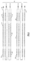
- a core 17 is one of several cores 18 , 19 and 20 with patterns of copper lines.
- a bottom layer 21 is illustrated on the bottom of the lower core 20 . Therefore, the printed circuit board 10 is formed of the top layer 16 , the cores 17 through 20 and the bottom layer 21 . There are intervening layers of a dielectric material, but these will be described in more detail hereinafter.
- power circuit areas 22 and 23 at the lower surface of the core 18 are located with signal lines 24 and that these lines are spaced from lines 25 , 26 and 27 in a comparable circuit pattern at the top surface of the core 19 .
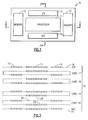
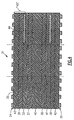
- FIG. 3 of the drawings the same printed circuit board 10 is illustrated along line 3-3 in FIG. 1. Also, in this view, the top layer 16 reveals the circuit lines 14, 11 and 15 as seen looking from top to bottom in FIG. 1 .
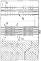
- FIG. 3 A particular feature that is available with a printed circuit board that is constructed and arranged in accordance with the principles of the invention is illustrated in both of these FIGs. 2 and 3 .
- a power circuit area 28 in any particular pattern, is spaced from a signal circuit line 29 not only by a blank space 30 at the top surface of the core 20 , but also by the precalculated thickness of an intervening dielectric layer. This will become clearer as the description proceeds.
- circuit packaging requirements can be controlled by the spacing between various conductors and other components. For example, the thickness of a dielectric between a signal plane and a power plane can produce a dramatic affect on noise.
Landscapes
- Engineering & Computer Science (AREA)
- Microelectronics & Electronic Packaging (AREA)
- Manufacturing & Machinery (AREA)
- Production Of Multi-Layered Print Wiring Board (AREA)
Applications Claiming Priority (2)
| Application Number | Priority Date | Filing Date | Title |
|---|---|---|---|
| US7454793A | 1993-06-11 | 1993-06-11 | |
| US74547 | 1993-06-11 |
Publications (2)
| Publication Number | Publication Date |
|---|---|
| EP0629107A2 true EP0629107A2 (fr) | 1994-12-14 |
| EP0629107A3 EP0629107A3 (fr) | 1995-09-13 |
Family
ID=22120147
Family Applications (1)
| Application Number | Title | Priority Date | Filing Date |
|---|---|---|---|
| EP94108594A Withdrawn EP0629107A3 (fr) | 1993-06-11 | 1994-06-01 | Technique de panneaux à cristaux imprimés à câblage et coupe transversale multiple. |
Country Status (3)
| Country | Link |
|---|---|
| US (1) | US5418690A (fr) |
| EP (1) | EP0629107A3 (fr) |
| JP (1) | JP2513443B2 (fr) |
Cited By (1)
| Publication number | Priority date | Publication date | Assignee | Title |
|---|---|---|---|---|
| FR2735324A1 (fr) * | 1995-06-08 | 1996-12-13 | Nec Corp | Carte de cablage stratifiee |
Families Citing this family (22)
| Publication number | Priority date | Publication date | Assignee | Title |
|---|---|---|---|---|
| JPH09232697A (ja) * | 1996-02-20 | 1997-09-05 | Canon Inc | プリント配線板 |
| US5841074A (en) * | 1996-03-12 | 1998-11-24 | International Business Machines Corporation | Backplane power distribution system having impedance variations in the form of spaced voids |
| US6727435B1 (en) * | 1996-03-12 | 2004-04-27 | International Business Machines Corporation | Backplane power distribution system |
| US5912809A (en) * | 1997-01-21 | 1999-06-15 | Dell Usa, L.P. | Printed circuit board (PCB) including channeled capacitive plane structure |
| US6150895A (en) * | 1999-01-25 | 2000-11-21 | Dell Usa, L.P. | Circuit board voltage plane impedance matching |
| JP3924126B2 (ja) * | 2001-01-16 | 2007-06-06 | アルプス電気株式会社 | プリント配線基板、及びその製造方法 |
| US6495772B2 (en) * | 2001-04-12 | 2002-12-17 | International Business Machines Corporation | High performance dense wire for printed circuit board |
| US6583498B1 (en) | 2002-08-09 | 2003-06-24 | International Business Machine Corporation | Integrated circuit packaging with tapered striplines of constant impedance |
| US6828514B2 (en) * | 2003-01-30 | 2004-12-07 | Endicott Interconnect Technologies, Inc. | High speed circuit board and method for fabrication |
| US6995322B2 (en) * | 2003-01-30 | 2006-02-07 | Endicott Interconnect Technologies, Inc. | High speed circuitized substrate with reduced thru-hole stub, method for fabrication and information handling system utilizing same |
| US7023707B2 (en) * | 2003-01-30 | 2006-04-04 | Endicott Interconnect Technologies, Inc. | Information handling system |
| CA2455024A1 (fr) * | 2003-01-30 | 2004-07-30 | Endicott Interconnect Technologies, Inc. | Module electronique a puces empilees dote d'un porte-puces stratifie et methode de fabrication |
| US7035113B2 (en) * | 2003-01-30 | 2006-04-25 | Endicott Interconnect Technologies, Inc. | Multi-chip electronic package having laminate carrier and method of making same |
| US6928726B2 (en) * | 2003-07-24 | 2005-08-16 | Motorola, Inc. | Circuit board with embedded components and method of manufacture |
| US7583513B2 (en) * | 2003-09-23 | 2009-09-01 | Intel Corporation | Apparatus for providing an integrated printed circuit board registration coupon |
| US7161088B2 (en) * | 2003-12-04 | 2007-01-09 | Dell Products L.P. | System, method and apparatus for optimizing power delivery and signal routing in printed circuit board design |
| US7378598B2 (en) * | 2004-02-19 | 2008-05-27 | Hewlett-Packard Development Company, L.P. | Printed circuit board substrate and method for constructing same |
| US7292452B2 (en) * | 2004-06-10 | 2007-11-06 | Intel Corporation | Reference layer openings |
| US7345889B1 (en) * | 2004-09-28 | 2008-03-18 | Avaya Technology Corp. | Method and system for reducing radiated energy emissions in computational devices |
| US7286366B2 (en) * | 2005-03-24 | 2007-10-23 | Motorola, Inc. | Multilayer circuit board with embedded components and method of manufacture |
| CN101472386B (zh) * | 2007-12-26 | 2012-03-28 | 鸿富锦精密工业(深圳)有限公司 | 印刷电路板 |
| EP3261417A1 (fr) * | 2016-06-22 | 2017-12-27 | OSRAM GmbH | Structure de support pour dispositifs d'éclairage, dispositif et procédé d'éclairage correspondants |
Family Cites Families (20)
| Publication number | Priority date | Publication date | Assignee | Title |
|---|---|---|---|---|
| US3436819A (en) * | 1965-09-22 | 1969-04-08 | Litton Systems Inc | Multilayer laminate |
| US3519959A (en) * | 1966-03-24 | 1970-07-07 | Burroughs Corp | Integral electrical power distribution network and component mounting plane |
| US3516156A (en) * | 1967-12-11 | 1970-06-23 | Ibm | Circuit package assembly process |
| US3616532A (en) * | 1970-02-02 | 1971-11-02 | Sperry Rand Corp | Multilayer printed circuit electrical interconnection device |
| JPS58180094A (ja) * | 1982-04-16 | 1983-10-21 | 株式会社日立製作所 | 多層プリント配線板の製造方法 |
| US4659931A (en) * | 1985-05-08 | 1987-04-21 | Grumman Aerospace Corporation | High density multi-layered integrated circuit package |
| US4849284A (en) * | 1987-02-17 | 1989-07-18 | Rogers Corporation | Electrical substrate material |
| JPS63249394A (ja) * | 1987-04-06 | 1988-10-17 | 日本電気株式会社 | 多層回路基板 |
| US4755911A (en) * | 1987-04-28 | 1988-07-05 | Junkosha Co., Ltd. | Multilayer printed circuit board |
| US4967314A (en) * | 1988-03-28 | 1990-10-30 | Prime Computer Inc. | Circuit board construction |
| JPH02164098A (ja) * | 1988-12-19 | 1990-06-25 | Fujitsu Ltd | プリント基板の特性インピーダンスの修正方法 |
| JP2793824B2 (ja) * | 1989-01-11 | 1998-09-03 | イビデン株式会社 | 電子回路基板 |
| JPH02277286A (ja) * | 1989-04-19 | 1990-11-13 | Hitachi Ltd | 多層プリント基板 |
| JPH03178193A (ja) * | 1989-12-07 | 1991-08-02 | Hitachi Ltd | 多層プリント基板 |
| JPH03231497A (ja) * | 1990-02-07 | 1991-10-15 | Nec Corp | 多層プリント配線板 |
| JPH0485991A (ja) * | 1990-07-27 | 1992-03-18 | Fujitsu Ltd | 多層プリント配線板の積層制御方法 |
| JPH04340795A (ja) * | 1991-05-17 | 1992-11-27 | Mitsubishi Electric Corp | プリント配線板 |
| JPH04364092A (ja) * | 1991-06-11 | 1992-12-16 | Sony Corp | 多層基板 |
| JP2654414B2 (ja) * | 1991-07-19 | 1997-09-17 | 沖電気工業株式会社 | 高速信号伝送用回路基板 |
| JP3097975U (ja) * | 2003-04-18 | 2004-02-12 | 株式会社東洋高圧 | 圧力調整器 |
-
1994
- 1994-03-10 JP JP6065472A patent/JP2513443B2/ja not_active Expired - Lifetime
- 1994-06-01 EP EP94108594A patent/EP0629107A3/fr not_active Withdrawn
- 1994-09-20 US US08/309,554 patent/US5418690A/en not_active Expired - Fee Related
Cited By (1)
| Publication number | Priority date | Publication date | Assignee | Title |
|---|---|---|---|---|
| FR2735324A1 (fr) * | 1995-06-08 | 1996-12-13 | Nec Corp | Carte de cablage stratifiee |
Also Published As
| Publication number | Publication date |
|---|---|
| US5418690A (en) | 1995-05-23 |
| JP2513443B2 (ja) | 1996-07-03 |
| JPH0715148A (ja) | 1995-01-17 |
| EP0629107A3 (fr) | 1995-09-13 |
Similar Documents
| Publication | Publication Date | Title |
|---|---|---|
| US5418690A (en) | Multiple wiring and X section printed circuit board technique | |
| US4799128A (en) | Multilayer printed circuit board with domain partitioning | |
| CA1143862A (fr) | Semiconducteur haute performance | |
| US5677515A (en) | Shielded multilayer printed wiring board, high frequency, high isolation | |
| US7530167B2 (en) | Method of making a printed circuit board with low cross-talk noise | |
| US4581679A (en) | Multi-element circuit construction | |
| US5262590A (en) | Impedance controlled flexible circuits with fold-over shields | |
| US4553111A (en) | Printed circuit board maximizing areas for component utilization | |
| US5446243A (en) | Post processing shielding | |
| US4237522A (en) | Chip package with high capacitance, stacked vlsi/power sheets extending through slots in substrate | |
| US4772864A (en) | Multilayer circuit prototyping board | |
| US5245135A (en) | Stackable high density interconnection mechanism (SHIM) | |
| US6815621B2 (en) | Chip scale package, printed circuit board, and method of designing a printed circuit board | |
| JP2001036247A (ja) | 多層配線基板 | |
| US5397861A (en) | Electrical interconnection board | |
| JP3899059B2 (ja) | 低抵抗高密度信号線をする電子パッケージおよびその製造方法 | |
| JPH04307799A (ja) | 特に高周波動作用の多層印刷回路板 | |
| US4361634A (en) | Artwork master for production of multilayer circuit board | |
| US6757175B1 (en) | Method and embedded bus bar structure for implementing power distribution | |
| US6365839B1 (en) | Multi-layer printed circuit board with dual impedance section | |
| US6351391B1 (en) | Signal busses on printed board structures mounting ASIC chips with signal termination resistor devices using planar signal terminating devices | |
| US6727435B1 (en) | Backplane power distribution system | |
| EP0436848B1 (fr) | Conducteurs verticaux à impédance adaptée dans un substrat laminaire métal-diélectrique à multi-couches | |
| CA1260625A (fr) | Carte de circuits imprimes multicouche a partitionnement en domaines | |
| JPH0521927A (ja) | 平面回路板を用いたハーネス回路の接続方法 |
Legal Events
| Date | Code | Title | Description |
|---|---|---|---|
| PUAI | Public reference made under article 153(3) epc to a published international application that has entered the european phase |
Free format text: ORIGINAL CODE: 0009012 |
|
| AK | Designated contracting states |
Kind code of ref document: A2 Designated state(s): DE FR GB |
|
| 17P | Request for examination filed |
Effective date: 19950425 |
|
| PUAL | Search report despatched |
Free format text: ORIGINAL CODE: 0009013 |
|
| AK | Designated contracting states |
Kind code of ref document: A3 Designated state(s): DE FR GB |
|
| STAA | Information on the status of an ep patent application or granted ep patent |
Free format text: STATUS: THE APPLICATION IS DEEMED TO BE WITHDRAWN |
|
| 18D | Application deemed to be withdrawn |
Effective date: 19980103 |