EP0630102B1 - Amplificateur différentiel à grand gain, capable de réduire la tension de décolage - Google Patents
Amplificateur différentiel à grand gain, capable de réduire la tension de décolage Download PDFInfo
- Publication number
- EP0630102B1 EP0630102B1 EP94304269A EP94304269A EP0630102B1 EP 0630102 B1 EP0630102 B1 EP 0630102B1 EP 94304269 A EP94304269 A EP 94304269A EP 94304269 A EP94304269 A EP 94304269A EP 0630102 B1 EP0630102 B1 EP 0630102B1
- Authority
- EP
- European Patent Office
- Prior art keywords
- transistor
- drain
- transistors
- power supply
- collector
- Prior art date
- Legal status (The legal status is an assumption and is not a legal conclusion. Google has not performed a legal analysis and makes no representation as to the accuracy of the status listed.)
- Expired - Lifetime
Links
- 230000005669 field effect Effects 0.000 claims description 36
- 238000010586 diagram Methods 0.000 description 5
- 230000000694 effects Effects 0.000 description 3
- 238000000034 method Methods 0.000 description 2
- 238000013459 approach Methods 0.000 description 1
- 230000015556 catabolic process Effects 0.000 description 1
- 238000006731 degradation reaction Methods 0.000 description 1
- 238000003780 insertion Methods 0.000 description 1
- 230000037431 insertion Effects 0.000 description 1
- 238000004519 manufacturing process Methods 0.000 description 1
- 238000012545 processing Methods 0.000 description 1
- 238000012546 transfer Methods 0.000 description 1
Images



Classifications
-
- H—ELECTRICITY
- H03—ELECTRONIC CIRCUITRY
- H03F—AMPLIFIERS
- H03F3/00—Amplifiers with only discharge tubes or only semiconductor devices as amplifying elements
- H03F3/45—Differential amplifiers
- H03F3/45071—Differential amplifiers with semiconductor devices only
- H03F3/45076—Differential amplifiers with semiconductor devices only characterised by the way of implementation of the active amplifying circuit in the differential amplifier
- H03F3/45179—Differential amplifiers with semiconductor devices only characterised by the way of implementation of the active amplifying circuit in the differential amplifier using MOSFET transistors as the active amplifying circuit
-
- H—ELECTRICITY
- H03—ELECTRONIC CIRCUITRY
- H03F—AMPLIFIERS
- H03F3/00—Amplifiers with only discharge tubes or only semiconductor devices as amplifying elements
- H03F3/45—Differential amplifiers
- H03F3/45071—Differential amplifiers with semiconductor devices only
- H03F3/45076—Differential amplifiers with semiconductor devices only characterised by the way of implementation of the active amplifying circuit in the differential amplifier
- H03F3/4508—Differential amplifiers with semiconductor devices only characterised by the way of implementation of the active amplifying circuit in the differential amplifier using bipolar transistors as the active amplifying circuit
- H03F3/45085—Long tailed pairs
-
- H—ELECTRICITY
- H03—ELECTRONIC CIRCUITRY
- H03F—AMPLIFIERS
- H03F3/00—Amplifiers with only discharge tubes or only semiconductor devices as amplifying elements
- H03F3/45—Differential amplifiers
- H03F3/45071—Differential amplifiers with semiconductor devices only
- H03F3/45076—Differential amplifiers with semiconductor devices only characterised by the way of implementation of the active amplifying circuit in the differential amplifier
- H03F3/4508—Differential amplifiers with semiconductor devices only characterised by the way of implementation of the active amplifying circuit in the differential amplifier using bipolar transistors as the active amplifying circuit
- H03F3/45085—Long tailed pairs
- H03F3/45089—Non-folded cascode stages
-
- H—ELECTRICITY
- H03—ELECTRONIC CIRCUITRY
- H03F—AMPLIFIERS
- H03F3/00—Amplifiers with only discharge tubes or only semiconductor devices as amplifying elements
- H03F3/45—Differential amplifiers
- H03F3/45071—Differential amplifiers with semiconductor devices only
- H03F3/45076—Differential amplifiers with semiconductor devices only characterised by the way of implementation of the active amplifying circuit in the differential amplifier
- H03F3/45179—Differential amplifiers with semiconductor devices only characterised by the way of implementation of the active amplifying circuit in the differential amplifier using MOSFET transistors as the active amplifying circuit
- H03F3/45183—Long tailed pairs
-
- H—ELECTRICITY
- H03—ELECTRONIC CIRCUITRY
- H03F—AMPLIFIERS
- H03F2203/00—Indexing scheme relating to amplifiers with only discharge tubes or only semiconductor devices as amplifying elements covered by H03F3/00
- H03F2203/45—Indexing scheme relating to differential amplifiers
- H03F2203/45024—Indexing scheme relating to differential amplifiers the differential amplifier amplifying transistors are cascode coupled transistors
-
- H—ELECTRICITY
- H03—ELECTRONIC CIRCUITRY
- H03F—AMPLIFIERS
- H03F2203/00—Indexing scheme relating to amplifiers with only discharge tubes or only semiconductor devices as amplifying elements covered by H03F3/00
- H03F2203/45—Indexing scheme relating to differential amplifiers
- H03F2203/45224—One output of the differential amplifier being taken into consideration
-
- H—ELECTRICITY
- H03—ELECTRONIC CIRCUITRY
- H03F—AMPLIFIERS
- H03F2203/00—Indexing scheme relating to amplifiers with only discharge tubes or only semiconductor devices as amplifying elements covered by H03F3/00
- H03F2203/45—Indexing scheme relating to differential amplifiers
- H03F2203/45244—Indexing scheme relating to differential amplifiers the differential amplifier contains one or more explicit bias circuits, e.g. to bias the tail current sources, to bias the load transistors
-
- H—ELECTRICITY
- H03—ELECTRONIC CIRCUITRY
- H03F—AMPLIFIERS
- H03F2203/00—Indexing scheme relating to amplifiers with only discharge tubes or only semiconductor devices as amplifying elements covered by H03F3/00
- H03F2203/45—Indexing scheme relating to differential amplifiers
- H03F2203/45471—Indexing scheme relating to differential amplifiers the CSC comprising one or more extra current sources
-
- H—ELECTRICITY
- H03—ELECTRONIC CIRCUITRY
- H03F—AMPLIFIERS
- H03F2203/00—Indexing scheme relating to amplifiers with only discharge tubes or only semiconductor devices as amplifying elements covered by H03F3/00
- H03F2203/45—Indexing scheme relating to differential amplifiers
- H03F2203/45732—Indexing scheme relating to differential amplifiers the LC comprising a voltage generating circuit
Definitions
- the present invention relates to a differential amplifier having high gain at a low frequency signal input.
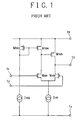
- Fig. 1 shows a conventional typical differential amplifier as disclosed in JP-A-6-045844.
- a pair of FETS (field-effect transistors) M101 and M102 whose sources are coupled with each other in common and whose gates are connected to respective input terminals t1 and t2 constitute a differential transistor pair.
- One end of a first constant-current source I101 is coupled with the common source connection point of the FETs M101 and M102 and the other end of the first constant-current source I101 is connected to a low power supply terminal t4.
- the drain and gate of an FET M103 are coupled with each other and the source of the FET M103 is connected to a high power supply terminal t5.
- the gate of another FET M104 is connected to the gate of the FET M103, and the source to the high power supply terminal t5, and the drain to the drain of the FET M101.
- the FETs M103 and M104 constitute a current mirror circuit.
- the gate of an FET M105 is connected to the drains of the FETs M101 and M104, and the source to the high power supply terminal t5, and the drain to an output terminal t3 and to the drain of the FET M102.
- One end of a second constant-current source I102 is coupled with the drain and gate of the FET M103 and the other end to the low power supply terminal t4.
- the differential transistor pair composed of the FETs M101 and M102 distributes the current of the first constant-current source I101 depending on signal voltages applied to the input terminals t1 and t2 to flow a drain current.
- the current mirror circuit including the FETs M103 and M104 outputs a current which is fixed and equal to the current value determined by the second constant-current source I102 and hence the variation of the drain current of the FET M101 is transferred to the gate of the FET M105.
- the variation of the drain current of the FET M101 is amplified by the FET M105 and the amplified current is output from the output terminal t3.
- the variation of the drain current of the FET M102 turns to a value to negate the variation of the drain current of the FET M101 and is also picked up from the output terminal t3.
- Fig. 1 discloses the differential amplifier having large voltage gain.
- the conventional differential amplifier has the large voltage gain, the difference of the operating point voltage among the transistors causes a difference in a balance point operating current of the differential transistor pair and as a result, an input offset voltage occurs. That is, in the conventional differential amplifier shown in Fig. 1, the current value of the first constant-current source I101 is set to twice as much as that of the second constant-current source I102 and the same transistor is used for the FETs M103 and M104 so that the operating point current of the two FETs M101 and M102 constituting the differential pair may be equal.
- a differential amplifier comprising a current mirror circuit; a differential transistor pair including first and second transistors connected to first and second input terminals, respectively, for distributing current depending on signal voltages applied to the first and second input terminals; a first constant-current source for supplying the current to be distributed by the differential transistor pair, one end and another end of which are connected to the differential transistor pair and to a first power supply terminal, respectively; a third field-effect transistor whose drain and gate are coupled and whose source is connected to a second power supply terminal; and a fourth field-effect transistor whose gate, source and drain are connected to the gate and drain of the third field-effect transistor, to the second power supply terminal and to the first transistor, respectively; a fifth field-effect transistor whose gate, source and drain are connected to the first transistor and the drain of the fourth field-effect transistor, to the second power supply terminal and to an output terminal and the second transistor, respectively; a sixth transistor which is connected to the gate and drain of the third field-effect transistor and
- the first and second transistors of the differential transistor pair are field-effect transistors whose gates are connected to the respective first and second input terminals and whose sources are coupled in common with one end of the first power supply terminal, and a drain of the first field-effect transistor is connected to the drain of the fourth field-effect transistor.
- the drains of the first and fourth field-effect transistors are connected to the gate of the fifth field-effect transistor, and a drain of the second field-effect transistor is coupled with the output terminal and the drain of the fifth field-effect transistor.
- the sixth transistor is a field-effect transistor whose drain, source and gate are connected to the gate and drain of the third field-effect transistor, to one end of the second constant-current source and to the third power supply terminal, respectively.
- the first and second transistors of the differential transistor pair are bipolar transistors whose bases are connected to the respective first and second input terminals and whose emitters are coupled in common with one end of the first power supply terminal, and a collector of the first bipolar transistor is connected to the drain of the fourth field-effect transistor.
- the collector of the first bipolar transistor and the drain of the fourth field-effect transistor are connected to the gate of the fifth field-effect transistor, and a collector of the second bipolar transistor is coupled with the output terminal and the drain of the fifth field-effect transistor.
- the sixth transistor is a bipolar transistor whose collector whose collector, emitter and base are connected to the gate and drain of the third field-effect transistor, to one end of the second constant-current source and to the third power supply terminal, respectively.
- a differential amplifier comprising a current mirror circuit; a differential transistor pair including first and second bipolar transistors whose emtters are coupled in common and whose bases are connected to first and second input terminals, respectively; a first constant-current source, one end and another end of which are connected to the common emitters of the first and second bipolar transistors of the differential transistor pair and to a first power supply terminal, respectively; a pair of third and fourth bipolar transistors whose bases are coupled in common with a second power supply terminal and whose emitters are connected to collectors of the respective first and second bipolar transistors; a first field-effect transistor whose drain and gate are coupled and whose source is connected to a third power supply terminal; and a second field-effect transistor whose gate, source and drain are connected to the gate and drain of the first field-effect transistor, to the third power supply terminal and to a collector of the third bipolar transistor, respectively; a third field-effect transistor whose gate, source and drain are connected to
- a differential amplifier comprising a current mirror circuit; a differential transistor pair including first and second bipolar transistors whose emitters are coupled in common and whose bases are connected to first and second input terminals, respectively; a first constant-current source, one end and another end of which are connected to the common emitters of the first and second bipolar transistors of the differential transistor pair and to a first power supply terminal, respectively; a pair of third and fourth bipolar transistors whose bases are coupled in common with a second power supply terminal and whose emitters are connected to collectors of the respective first and second bipolar transistors; a fifth bipolar transistor whose collector and base are coupled and whose emitter is connected to a third power supply terminal; and a sixth bipolar transistor whose base, emmiter and collector are connected to the collector and base of the fifth bipolar transistor, to the third power supply terminal and to a collector of the third bipolar transistor, respectively; a seventh bipolar transistor whose base, emitter and collector are connected
- Fig. 2 there is shown the first embodiment differential amplifier according to the present invention.
- a differential transistor pair is composed of first and second FETs M1 and M2 whose sources are coupled with each other in common and whose gates are connected to first and second input terminals t1 and t2, respectively.
- One end of a first constant-current source I1 is connected to the common sources of the FETs M1 and M2 and the other end to a low power supply terminal t4.
- the drain and gate of a third FET M3 is coupled with each other and the source of the same is connected to a high power supply terminal t5.
- the gate of a fourth FET M4 is coupled with the gate of the third FET M3, and the source with the high power supplhy terminal t5, and the drain with the drain of the first FET M1.
- the third and fourth FETs M3 and M4 constitute a current mirror circuit.
- the gate of a fifth FET M5 is connected to the drains of the first and fourth FETs M1 and M4, and the source to the high power supply terminal t5, and the drain to an output terminal t3 and to the drain of the second FET M2.
- the drain of a sixth FET M6 is connected to the drain of the third FET M3, and the gate to a bias power supply terminal t6.
- One end of a second constant-current source I2 is connected to the source of the sixth FET M6 and the other end of the same to the low power supply terminal t4.
- the differential transistor pair composed of the first and second FETs M1 and M2 distributes the current of the first constant-current source I1 depending on the signal voltages applied to the first and second input terminals t1 and t2 to flow the drain current.
- the current mirror circuit including the third and fourth FETs M3 and M4 outputs a current which is fixed and equal to the current value determined by the second constant-current source I2 and the sixth FET M6 and hence the variation of the drain current of the first FET M1 is transferred to the gate of the fifth FET M5.
- the variation of the drain current of the first FET M1 is amplified by the fifth FET M5 and the amplified current is output from the output terminal t3.
- the variation of the drain current of the second FET M2 turns to a value to negate the variation of the drain current of the first FET M1. That is, the drain current of the second FET M2 reduces in proportion to the increase of the drain current of the first FET M1.
- AV (1/2) ⁇ gm1 ⁇ ⁇ ro1 ⁇ ro4 ⁇ ri5/(ro1 ⁇ ro4 + ro4 ⁇ ri5 + ri5 ⁇ ro1) ⁇ ⁇ gm5 ⁇ ⁇ ro2 ⁇ ro5/(ro2 + ro5) ⁇ + (1/2) ⁇ gm2 ⁇ ⁇ ro2 ⁇ ro5/(ro2 + ro5) ⁇ wherein gm1, gm2 and gm5 represent transfer conductances of the first, second and fifth FETs M1, M2 and M5, respectively, and ro1, ro2, ro4 and ro5 represent output resistances of the first, second, fourth and fifth FETs M1, M2, M4 and M5, respectively, and ri5
- the differential amplifier shown in Fig. 2 has a very large voltage gain AV of approximately 91 [dB] in the low frequency.
- the current value of the first constant-current source I1 is determined to twice as much as that of the second constant-current source I2 and the same transistor is used for the third and fourth FETs M3 and M4 so that the operating point current of the first and second FETs M1 and M2 constituting the differential transistor pair may be equal.
- the insertion of the sixth FET M6 between the second constant-current source I2 and the pair of third and fourth FETs M3 and M4 of the current mirror circuit permits the voltages between the drain and source of the third and fourth FETs M3 and M4 to be nearly equal and hence the input offset voltage between the first and second input terminals t1 and t2 can be made nearly zero in the differential amplifier.
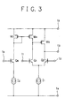
- Fig. 3 shows the second embodiment of a differential amplifier according to the present invention.
- first, second and sixth bipolar transistors Q1, Q2 and Q6 are used in place of the respective first, second and sixth FETs M1, M2 and M6 of the first embodiment described above.
- bipolar transistors have a better pair matching in integrated circuits than field-effect transistors.
- the input offset voltage can approach more close to zero.
- Fig. 4 illustrates the third embodiment of a differential amplifier according to the present invention.
- third, fourth and eighth bipolar transistors Q3, Q4 and Q8 whose bases are coupled with another bias power supply terminal t7 are inserted between the first bipolar transistor Q1 and the fourth FET M4, between the second bipolar transistor Q2 and the fifth FET M5, and between the sixth bipolar transistor Q6 and the third FET M3, respectively.
- the addition of the pair of common base transistors Q3 and Q4 to the differential transistor pair of the first and second bipolar transistors Q1 and Q2 permits the increase of the voltage gain and further remarkable improvement against frequency characteristic degradation due to a Miller capacitance at the input terminal portions in addition to the effects obtained in the second embodiment shown in Fig. 3.
- Fig. 5 shows the fourth embodiment of a differential amplifier according to the present invention.
- bipolar transistors Q15, Q16 and Q17 are used in place of the third, fourth and fifth FETs M3, M4 and M5 of the third embodiment shown in Fig. 4. In this case, the same effects as described above can also be obtained.
- the differential amplifier can be produced by a pure bipolar process, it is possible to provide a high gain, high speed, low offset differential amplifier at a lower cost.
- bipolar transistors, the field-effect transistors and the constant-current sources can, of course, be arranged in the reversed polarity in the circuits shown in Fig. 2 to Fig. 5 with the same effects.
- a differential amplifier which has a large voltage gain at a low frequency signal input and is capable of reducing the input offset voltage of the conventional problem to nearly zero can be obtained and as a result, can be applied to a high accuracy signal processing circuit.
Landscapes
- Engineering & Computer Science (AREA)
- Power Engineering (AREA)
- Amplifiers (AREA)
Claims (7)
- Amplificateur différentiel, comprenant :caractérisé en ce que l'amplificateur comprend, en outreune paire de transistors différentielle incluant des premier et second transistors (M1, Q1, M2, Q2) connectés à des première et seconde bornes d'entrée (t1, t2), respectivement, pour distribuer le courant en fonction du signal de tension aux première et seconde bornes d'entrée (t1, t2), respectivement ;une première source de courant constant (I1) pour fournir le courant devant être distribué par la paire de transistors différentielle ;un circuit miroir de courant comprenant : un troisième transistor (M3, Q15) dont le drain ou le collecteur et la grille ou la base sont connectés ensemble et dont la source ou l'émetteur est connecté à une seconde borne d'alimentation (t5), et un quatrième transistor (M4, Q16) dont la grille ou la base, la source ou l'émetteur et le drain ou le collecteur sont respectivement connectés à la gille ou la base du troisième transistor, à la seconde alimentation et au premier transistor ;une seconde source de courant constant (I2) connectée en série au troisième transistor ;des moyens amplificateurs pour délivrer une caractéristique de sortie amplifiée de la différence entre le courant distribué, comprenant un cinquième transistor (M5, Q17) dont la grille ou la base, la source ou l'émetteur et le drain ou le collecteur sont respectivement connectés à la jonction entre le premier transistor et le drain ou le collecteur du quatrième transistor, à la seconde borne d'alimentation, et à une borne de sortie (t5), de sorte que la borne de sortie est connectée au second transistor ;des moyens égalisateurs (M6, Q6) pour égaliser les tensions entre les drains ou les collecteurs et les sources ou les émetteurs respectifs des troisième et quatrième transistors, de manière à rendre ainsi minimale une tension de décalage entre les première et seconde bornes d'entrée (t1, t2).
- Amplificateur différentiel selon la revendication 1, dans lequel la première source de courant constant (I1) comporte une borne connectée à la paire de transistors différentielle et l'autre borne connectée à une première borne d'alimentation (t4) ;lesdits moyens égalisateurs égalisant les tensions entre les troisième et quatrième transistors étant un sixième transistor (M6, Q16) dont le drain ou le collecteur est connecté au drain ou au collecteur du troisième transistor et dont la grille ou la base est connectée à une troisième borne d'alimentation (t6) ; etune seconde source de courant constant (I2) dont une première borne et une autre borne sont connectées à la source ou à l'émetteur du sixième transistor et à la première borne d'alimentation (t4), respectivement.
- Amplificateur différentiel selon la revendication 2, caractérisé en ce que les troisième, quatrième et cinquième transistors sont des transistors à effet de champ (M3, M4, M5).
- Amplificateur différentiel selon la revendication 3, caractérisé en ce que les premier et second transistors de la paire de transistors différentielle sont des transistors à effet de champ (M1, M2) et le sixième transistor est un transistor à effet de champ (M6).
- Amplificateur différentiel selon la revendication 2, caractérisé en ce que les troisième, quatrième et cinquième transistors sont des transistors bipolaires (Q15, Q16, Q17).
- Amplificateur différentiel selon la revendication 3 ou 5, caractérisé en ce que les premier et second transistors de la paire de transistors différentielle sont des transistors bipolaires (Q1, Q2) et le sixième transistor est un transistor bipolaire (Q6).
- Amplificateur différentiel selon la revendication 6, comprenant, en outre, trois transistors bipolaires supplémentaires (Q3, Q4, Q8), dans lequel :les collecteurs desdits premier, second et sixième transistors (Q1, Q2, Q6) sont, à la place, connectés aux émetteurs desdits troisième, quatrième et huitième transistors bipolaires (Q3, Q4, Q8), respectivement ;Le collecteur dudit troisième transistor bipolaire (Q3) est connecté au drain du quatrième transistor à effet de champ (M4) ;le collecteur du quatrième transistor bipolaire est couplé à la borne de sortie (t3) et au drain du cinquième transistor à effet de champ (M5) ;le collecteur du huitième transistor bipolaire (Q8) est connecté à la grille et au drain du troisième transistor à effet de champ (M3); etles bases desdits troisième, quatrième et huitième transistors (Q3, Q4, Q8) sont connectées à une quatrième borne d'alimentation (t7).
Applications Claiming Priority (2)
| Application Number | Priority Date | Filing Date | Title |
|---|---|---|---|
| JP5143894A JP2590685B2 (ja) | 1993-06-15 | 1993-06-15 | 差動増幅器 |
| JP143894/93 | 1993-06-15 |
Publications (3)
| Publication Number | Publication Date |
|---|---|
| EP0630102A2 EP0630102A2 (fr) | 1994-12-21 |
| EP0630102A3 EP0630102A3 (fr) | 1995-08-23 |
| EP0630102B1 true EP0630102B1 (fr) | 1999-05-06 |
Family
ID=15349526
Family Applications (1)
| Application Number | Title | Priority Date | Filing Date |
|---|---|---|---|
| EP94304269A Expired - Lifetime EP0630102B1 (fr) | 1993-06-15 | 1994-06-14 | Amplificateur différentiel à grand gain, capable de réduire la tension de décolage |
Country Status (4)
| Country | Link |
|---|---|
| US (1) | US5396191A (fr) |
| EP (1) | EP0630102B1 (fr) |
| JP (1) | JP2590685B2 (fr) |
| DE (1) | DE69418250T2 (fr) |
Families Citing this family (2)
| Publication number | Priority date | Publication date | Assignee | Title |
|---|---|---|---|---|
| WO2003079623A1 (fr) * | 2002-03-15 | 2003-09-25 | Gennum Corporation | Systeme et procede de compensation d'affaiblissement de la ligne sur une liaison d'interface visuelle numerique (dvi) |
| US8629726B1 (en) * | 2011-04-29 | 2014-01-14 | Bae Systems Information And Electronic Systems Integration Inc. | High-performance amplifier for transducer array input unit cell |
Citations (1)
| Publication number | Priority date | Publication date | Assignee | Title |
|---|---|---|---|---|
| JPH0645844A (ja) * | 1992-02-27 | 1994-02-18 | Nec Corp | 差動増幅器 |
Family Cites Families (8)
| Publication number | Priority date | Publication date | Assignee | Title |
|---|---|---|---|---|
| JPS57194610A (en) * | 1981-05-26 | 1982-11-30 | Nippon Telegr & Teleph Corp <Ntt> | Differential amplifier |
| JPS61139107A (ja) * | 1984-12-11 | 1986-06-26 | Nec Corp | 演算増幅器 |
| US4658157A (en) * | 1985-05-31 | 1987-04-14 | Rca Corporation | IGFET comparator circuit having greater control of intended offset voltage |
| JPS62179207A (ja) * | 1986-02-03 | 1987-08-06 | Toshiba Corp | トランジスタ増幅器のオフセツト補正回路 |
| JPH01137708A (ja) * | 1987-11-24 | 1989-05-30 | Nec Corp | 増幅回路 |
| US5045806A (en) * | 1988-04-17 | 1991-09-03 | Teledyne Industries | Offset compensated amplifier |
| JPH0410705A (ja) * | 1990-04-27 | 1992-01-14 | Canon Inc | 差動増幅器 |
| JP2711411B2 (ja) * | 1990-09-07 | 1998-02-10 | 新日本無線株式会社 | 演算増幅回路 |
-
1993
- 1993-06-15 JP JP5143894A patent/JP2590685B2/ja not_active Expired - Lifetime
-
1994
- 1994-06-10 US US08/258,226 patent/US5396191A/en not_active Expired - Lifetime
- 1994-06-14 DE DE69418250T patent/DE69418250T2/de not_active Expired - Fee Related
- 1994-06-14 EP EP94304269A patent/EP0630102B1/fr not_active Expired - Lifetime
Patent Citations (1)
| Publication number | Priority date | Publication date | Assignee | Title |
|---|---|---|---|---|
| JPH0645844A (ja) * | 1992-02-27 | 1994-02-18 | Nec Corp | 差動増幅器 |
Also Published As
| Publication number | Publication date |
|---|---|
| DE69418250T2 (de) | 1999-09-02 |
| JP2590685B2 (ja) | 1997-03-12 |
| JPH077336A (ja) | 1995-01-10 |
| DE69418250D1 (de) | 1999-06-10 |
| EP0630102A3 (fr) | 1995-08-23 |
| EP0630102A2 (fr) | 1994-12-21 |
| US5396191A (en) | 1995-03-07 |
Similar Documents
| Publication | Publication Date | Title |
|---|---|---|
| US5608352A (en) | Differential input circuit capable of broadening operation range of input common mode potential | |
| EP0159757B1 (fr) | Amplificateur à excursion d'entrée couvrant la tension d'alimentation et transconductance réglée | |
| US5483194A (en) | Differential current mode amplifier device | |
| US5994959A (en) | Linearized amplifier core | |
| EP0058448A1 (fr) | Amplificateur à transconductance | |
| KR20020028783A (ko) | 선형 가변 이득 증폭기 | |
| EP0481631B1 (fr) | Etage de transconductance à large gamme dynamique | |
| US5170133A (en) | Low-noise amplifier with high input impedance, particularly for microphones | |
| US4893091A (en) | Complementary current mirror for correcting input offset voltage of diamond follower, especially as input stage for wide-band amplifier | |
| EP0874451A2 (fr) | Amplificateur à gain variable | |
| US5777514A (en) | Differential to single ended conversion technique for an operational amplifier having low input offset voltage, high speed and high gain | |
| US4419631A (en) | Integrated circuit amplifier functioning in class AB and incorporating CMOS (metal oxide semiconductor) technology | |
| US4004245A (en) | Wide common mode range differential amplifier | |
| US4451800A (en) | Input bias adjustment circuit for amplifier | |
| US4774478A (en) | Feedback amplifier compensation circuitry | |
| JPH07142940A (ja) | Mosfet電力増幅器 | |
| US5132640A (en) | Differential current amplifier circuit | |
| US5396191A (en) | High gain differential amplifier capable of reducing offset voltage | |
| JPH1197774A (ja) | 出力回路装置 | |
| US4603267A (en) | Low offset single ended MOS comparator | |
| JP2897724B2 (ja) | 差動増幅器 | |
| JP2877033B2 (ja) | 演算増幅回路 | |
| US5869957A (en) | Voltage divider circuit, differential amplifier circuit and semiconductor integrated circuit device | |
| US5170134A (en) | Fast buffer | |
| US5334949A (en) | Differential amplifiers |
Legal Events
| Date | Code | Title | Description |
|---|---|---|---|
| PUAI | Public reference made under article 153(3) epc to a published international application that has entered the european phase |
Free format text: ORIGINAL CODE: 0009012 |
|
| AK | Designated contracting states |
Kind code of ref document: A2 Designated state(s): DE FR GB NL |
|
| PUAL | Search report despatched |
Free format text: ORIGINAL CODE: 0009013 |
|
| AK | Designated contracting states |
Kind code of ref document: A3 Designated state(s): DE FR GB NL |
|
| 17P | Request for examination filed |
Effective date: 19950731 |
|
| 17Q | First examination report despatched |
Effective date: 19970530 |
|
| GRAG | Despatch of communication of intention to grant |
Free format text: ORIGINAL CODE: EPIDOS AGRA |
|
| GRAG | Despatch of communication of intention to grant |
Free format text: ORIGINAL CODE: EPIDOS AGRA |
|
| GRAG | Despatch of communication of intention to grant |
Free format text: ORIGINAL CODE: EPIDOS AGRA |
|
| GRAH | Despatch of communication of intention to grant a patent |
Free format text: ORIGINAL CODE: EPIDOS IGRA |
|
| GRAH | Despatch of communication of intention to grant a patent |
Free format text: ORIGINAL CODE: EPIDOS IGRA |
|
| GRAA | (expected) grant |
Free format text: ORIGINAL CODE: 0009210 |
|
| AK | Designated contracting states |
Kind code of ref document: B1 Designated state(s): DE FR GB NL |
|
| REF | Corresponds to: |
Ref document number: 69418250 Country of ref document: DE Date of ref document: 19990610 |
|
| ET | Fr: translation filed | ||
| PLBE | No opposition filed within time limit |
Free format text: ORIGINAL CODE: 0009261 |
|
| STAA | Information on the status of an ep patent application or granted ep patent |
Free format text: STATUS: NO OPPOSITION FILED WITHIN TIME LIMIT |
|
| 26N | No opposition filed | ||
| REG | Reference to a national code |
Ref country code: GB Ref legal event code: IF02 |
|
| PGFP | Annual fee paid to national office [announced via postgrant information from national office to epo] |
Ref country code: NL Payment date: 20080603 Year of fee payment: 15 Ref country code: DE Payment date: 20080619 Year of fee payment: 15 |
|
| PGFP | Annual fee paid to national office [announced via postgrant information from national office to epo] |
Ref country code: FR Payment date: 20080617 Year of fee payment: 15 |
|
| PGFP | Annual fee paid to national office [announced via postgrant information from national office to epo] |
Ref country code: GB Payment date: 20080618 Year of fee payment: 15 |
|
| GBPC | Gb: european patent ceased through non-payment of renewal fee |
Effective date: 20090614 |
|
| NLV4 | Nl: lapsed or anulled due to non-payment of the annual fee |
Effective date: 20100101 |
|
| REG | Reference to a national code |
Ref country code: FR Ref legal event code: ST Effective date: 20100226 |
|
| PG25 | Lapsed in a contracting state [announced via postgrant information from national office to epo] |
Ref country code: FR Free format text: LAPSE BECAUSE OF NON-PAYMENT OF DUE FEES Effective date: 20090630 |
|
| PG25 | Lapsed in a contracting state [announced via postgrant information from national office to epo] |
Ref country code: GB Free format text: LAPSE BECAUSE OF NON-PAYMENT OF DUE FEES Effective date: 20090614 |
|
| PG25 | Lapsed in a contracting state [announced via postgrant information from national office to epo] |
Ref country code: DE Free format text: LAPSE BECAUSE OF NON-PAYMENT OF DUE FEES Effective date: 20100101 |
|
| PG25 | Lapsed in a contracting state [announced via postgrant information from national office to epo] |
Ref country code: NL Free format text: LAPSE BECAUSE OF NON-PAYMENT OF DUE FEES Effective date: 20100101 |