EP0633529A1 - Système d'émulation pour microordinateur - Google Patents
Système d'émulation pour microordinateur Download PDFInfo
- Publication number
- EP0633529A1 EP0633529A1 EP94110607A EP94110607A EP0633529A1 EP 0633529 A1 EP0633529 A1 EP 0633529A1 EP 94110607 A EP94110607 A EP 94110607A EP 94110607 A EP94110607 A EP 94110607A EP 0633529 A1 EP0633529 A1 EP 0633529A1
- Authority
- EP
- European Patent Office
- Prior art keywords
- mode
- central processing
- peripheral
- processing unit
- chip
- Prior art date
- Legal status (The legal status is an assumption and is not a legal conclusion. Google has not performed a legal analysis and makes no representation as to the accuracy of the status listed.)
- Granted
Links
Images


Classifications
-
- G—PHYSICS
- G06—COMPUTING OR CALCULATING; COUNTING
- G06F—ELECTRIC DIGITAL DATA PROCESSING
- G06F11/00—Error detection; Error correction; Monitoring
- G06F11/36—Prevention of errors by analysis, debugging or testing of software
- G06F11/362—Debugging of software
- G06F11/3648—Debugging of software using additional hardware
- G06F11/3652—Debugging of software using additional hardware in-circuit-emulation [ICE] arrangements
Definitions
- the present invention relates to a emulation system, and more specifically to a microcomputer emulation system which makes it easy to construct an emulation chip set.
- a development tool including a microcomputer emulation system for assisting development and debugging of user's programs has become important in the process of developing a microcomputer-applied system.
- microcomputers specialized to application fields ad/or application systems are mainly constituted of a ASIC (application specific integrated circuit) microcomputer in which a high performance CPU is integrated as a core element on a single chip together with various peripheral function units suitable or specialized to a maker or user.
- ASIC application specific integrated circuit
- the shown emulation system is generally designated with Reference Numeral 100, and comprises a CPU evaluation chip 101 including therein a CPU 104A.
- This CPU 104A performs the same operation as that of an internal CPU included in a actual developed microcomputer product, which will he called a "product chip”.
- the CPU evaluation chip 101 is connected through a peripheral bus 102 to a peripheral evaluation chip 103. Operation timings of the peripheral bus 102 to the peripheral evaluation chip 103 are entirely the same as those of an internal bus coupling between a internal CPU and a peripheral unit in the product chip.
- the evaluation chip 103 in the example shown in Figure 1 is constituted by the product chip itself.
- the product chip itself includes an internal CPU 104B and a peripheral function unit 105 included in the peripheral evaluation chip 103.
- the product chip has two kinds of operation mode, namely, a operation mode of the product chip itself and an evaluation operation mode.
- the CPU 104B is coupled through a internal bus 106 to the peripheral unit 105 as shown by the ghost line in Figure 1, so that a normal operation is performed.
- the CPU 104B is electrically isolated from the internal bus 106, and a portion of the internal bus 106 is coupled to the peripheral bus 102.
- the product chip operation mode and the evaluation operation mode of the product chip are alternatively designated through a mode designation terminal 107. For example, if the mode designation terminal 107 is set to a logic value "0" connected to ground, the product chip operation mode is designated. If the mode designation terminal 107 is set to a logic value "1" connected to a voltage supply voltage, the evaluation operation mode is designated. The evaluation chip 103 shown in Figure 1 is in the evaluation operation mode.
- various controls including a data read/write control
- various controls to the peripheral function unit are emulated in the emulation system by accessing through the peripheral bus 102 and the internal bus 106 to the peripheral function unit 105 internally provided in the peripheral evaluation chip 103, under instruction execution of the CPU 104A in the CPU evaluation chip 101.
- connection and access to an external memory and an I/O device are performed through a system bus 108 provided to the CPU evaluation chip 101.
- Terminal function corresponding to the peripheral function unit 105 is realized by a peripheral function signal 109 of the peripheral evaluation chip 103.
- the system bus 108 ad the peripheral function signal 109 are connected to an external through a system bus terminal 110 and a peripheral function terminal 111 of the emulation system 100.
- the peripheral evaluation chip 103 is made to cause only the peripheral function unit 105 to effectively operate for the product chip. Function of the product chip corresponding to terminals switched to the peripheral bus 102 is substituted with functions provided in the CPU evaluation chip 101.
- chip-set structure of emulation system 100 it is sufficient if only a product chip is developed for each application. Namely, it is unnecessary to develop a specialized evaluation chip for each application. Accordingly, it is advantageous in that an effective development environment is given to users.
- JP-A-03-058141 discloses a integrated circuit with a user's logic. This integrated circuit can be independently connected to respective external terminals, when an additional user's logic circuit is connected to the existing microcomputer.
- the user specific logic circuit has an extremely high level of versatility in comparison with the peripheral function units of the conventional ASIC microcomputers, so that it can be different not only from one user to another, but also from one instrument to another.
- how to construct a emulation system for emulating this integrated circuit with the user's logic has become a problem.
- FIG 2 there is shown a block diagram of an emulation system 200 constructed by adding a gate array 201 for a user specific logic circuit, to the emulation system 100 shown in Figure 1.
- the gate array 201 is newly developed independently of the product chip, and is required to be developed for each user and for each instrument, so as to correspond to a user specific logic circuit included in the product chip.
- the gate array 201 is connected to the CPU evaluation chip 101 through the system bus 108, so that various controls (including the data read/write control) to internal hardware are performed by instruction execution of the CPU.
- An internal circuit of the gate array 201 is constructed to be able to perform a operation equivalent to that of the user logic internally contained in the product chip.
- a user logic terminal 203 is provided for inputting and outputting a user logic signal to and from the gate array 201, so that the functions corresponding to the user logic circuit included in the product chip are emulated.
- the conventional emulation system has required to newly prepare a gate array corresponding to the user specific logic circuit.
- Another object of the present invention is to provide an emulation system capable of giving a completely satisfactory emulation environment, with no special gate array, by efficiently utilizing hardware resources.
- a further object of the present invention is to provide an inexpensive emulation system having a high level of utility and capable of giving a completely satisfactory emulation environment, with no special gate array, by efficiently utilizing hardware resources.
- an emulation system for emulating a microcomputer which includes a central processing unit, a peripheral function unit and a user specific logic circuit, which are integrated together on a single chip, the system including a first integrated circuit for emulating the central processing unit, a second integrated circuit operating in a first operation mode for emulating the peripheral function unit, and a third integrated circuit operating in a second operation mode for emulating the logic circuit, the first, second and third integrated circuits being interconnected, and each of the second and third integrated circuits having a mode designating means for switching between the first operation mode and the second operation mode.
- the mode designating means includes at least one mode designation terminal for designating the operation mode from an external.
- each of the second and third integrated circuits includes the same central processing unit, the same peripheral function unit and the same specific logic circuit as corresponding ones of the microcomputer.
- Each of the second and third integrated circuits is such that, when it is in the first operation mode, the central processing unit and the specific logic circuit are electrically isolated from an internal bus, and when it is in the second operation mode, the central processing unit and the peripheral function unit are electrically isolated from the internal bus.
- each of the second and third integrated circuits can have a third operation mode in which the central processing unit, the peripheral function unit and the specific logic circuit are electrically connected to the internal bus.
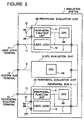
- FIG. 3 there is shown a block diagram of one embodiment of the emulation system in accordance with the present invention.
- the shown emulation system generally designated with Reference Numeral 1, includes a CPU evaluation chip 2, and two peripheral evaluation chips 4A and 4B.
- the CPU evaluation chip 2 internally contains a CPU 5A, which performs the same operation as that of an actual developed microcomputer product, namely a product chip.
- the CPU evaluation chip 2 is connected through a peripheral bus 3 to the peripheral evaluation chips 4A and 4B, respectively. Operating timing of the peripheral bus 3 to the peripheral evaluation chips 4A and 4B are entirely the same as those of an internal bus interconnecting between an internal CPU and a peripheral function unit in the product chip.
- each of the peripheral evaluation chips 4A and 4B is constituted of the product chip.
- the product chip includes an internal CPU 5B, a peripheral function unit 6 and a user logic 15 which are integrated on a single chip, and has three operation modes, namely, a product chip operation mode, a peripheral function evaluation mode and a user logic evaluation mode.
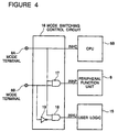
- TABLE 1 TABLE 1 MODE TERMINAL OPERATION MODE 8A 8B GND GND PRODUCT CHIP OPERATION MODE GND VCC (NO SETTING) VCC GND PERRPHERAL FUNCTION EVALUATION MODE VCC VCC USER LOGIC EVALUATION MODE
- a mode switching logic circuit used in each of the peripheral evaluation chips 4A and 48.
- a mode switching logic circuit generally designated with Reference Numeral 16, includes an AND gate 17 having a pair of inputs connected to the mode terminals 8A and 8B, respectively, an inverter 19 having an input connected to the mode terminal 8B, and another AND gate 18 having a pair of inputs connected to the mode terminal 8A and an output of the inverter 19, respectively.
- the mode terminal 8A is connected to the CPU 5B as a mode control signal INHC, and an output of the AND gate 17 is connected to the peripheral function unit 6 as a mode control signal INHP.
- An output of the AND gate 18 is connected to the user logic 15 as a mode control signal INHU.
- mode control signals are generated by connecting the mode terminals 8A and 8B to the voltage supply voltage (VCC) and ground (GND), as shown in the following TABLE 2: TABLE 2 MODE TERMINAL MODE CONTROL SIGNAL 8A 8B INHC INHP INHU GND GND 0 0 0 GND VCC 0 0 0 VCC GND 1 0 1 VCC VCC 1 1 0
- the CUP 5B, the peripheral function unit 6 and the user logic 15 are interconnected through the internal bus 7 so as to perform a normal operation.
- the CPU 5B and the user logic 15 are electrically isolated from the internal bus 7, and a portion of the internal bus 7 is connected to the peripheral bus 3.
- the CPU 5B and the peripheral function unit 6 are electrically isolated from the internal bus 7, and a portion of the internal bus 7 is connected to the peripheral bus 3.
- the operation mode of the product chip can be alternatively designated by the mode terminals 8A and 8B. Namely, the product chip can be put in the peripheral function evaluation mode or in the user logic evaluation mode.
- the peripheral evaluation chip 4A is put in the peripheral function evaluation mode so that only the peripheral function unit 6 of the product chip effectively operates
- the peripheral evaluation chip 4B is put in the user logic evaluation mode so that only the user logic 15 of the product chip effectively operates.
- various controls including data read/write control of the CPU to the user logic in the product chip are perfectly emulated in the emulation system 1, by accessing through the peripheral bus 3 and the internal bus 7 to the internal user logic 15 of the peripheral evaluation chip 4B under instruction execution of the CPU 5A in the CPU evaluation chip 2.
- connection and access to an external memory and an I/O device are performed through a system bus 9 provided to the CPU evaluation chip 2.
- Terminal function corresponding to the peripheral function unit 6 is realized by a peripheral function signal 10 of the peripheral evaluation chip 4A.
- Terminal function corresponding to the user logic 15 is realized by a user logic signal 11 of the peripheral evaluation chip 4B.
- the system bus 9, the peripheral function signal 10 ad the user logic signal 11 are connected to an external through a system bus terminal 12, a peripheral function terminal 13 and a user logic terminal 14 of the emulation system 1. Functions of these terminal are completely equivalent to those of the product chip.
- function of the peripheral evaluation chips 4A and 4B, namely the product chips, corresponding to terminals switched to the peripheral bus 3 is substituted with functions provided in the CPU evaluation chip 2,
- the above mentioned emulation system 1 has been configured so that the evaluation chip operation mode of the product chip is designated and switched over by the mode terminals 8A ad 8B.
- the present invention is not limited to this embodiment, For example, it is possible to provide a mode register within the emulation system 1 and to change the setting of the mode register in a software manner.
- mode setting can be performed by a parallel signal transmission through a plurality of terminals or a serial signal transmission through only one terminal.
- the evaluation chip operation mode is not necessarily limited to the two kinds, but can have three or more kinds by further dividing the peripheral function unit and the user logic so that the peripheral evaluation chip can be used in three or more different operation modes.
- the emulation system in accordance with the present invention makes it unnecessary to prepare or develop a gate array corresponding to the user specific logic. Namely, since the emulation system in accordance with the present invention utilizes the product chip as the user logic evaluation chip, when a microcomputer is developed, it becomes unnecessary to develop a gate array inherent to the developed microcomputer. Accordingly, the development steps and the development cost for designing, manufacturing and evaluating the gate array and the like become unnecessary. This is a remarkable advantage.
- the emulation system in accordance with the present invention can give an emulation environment which operates under perfectly the same condition as that of the product chip. Therefore, hardware resource can be efficiently utilized, and further, a perfect emulation environment can be realized. This is also a remarkable practical advantage.
Landscapes
- Engineering & Computer Science (AREA)
- Computer Hardware Design (AREA)
- Theoretical Computer Science (AREA)
- Quality & Reliability (AREA)
- Physics & Mathematics (AREA)
- General Engineering & Computer Science (AREA)
- General Physics & Mathematics (AREA)
- Test And Diagnosis Of Digital Computers (AREA)
- Microcomputers (AREA)
Applications Claiming Priority (2)
| Application Number | Priority Date | Filing Date | Title |
|---|---|---|---|
| JP191790/93 | 1993-07-07 | ||
| JP5191790A JPH0728665A (ja) | 1993-07-07 | 1993-07-07 | マイクロコンピュータ用エミュレーション装置 |
Publications (2)
| Publication Number | Publication Date |
|---|---|
| EP0633529A1 true EP0633529A1 (fr) | 1995-01-11 |
| EP0633529B1 EP0633529B1 (fr) | 1999-04-14 |
Family
ID=16280585
Family Applications (1)
| Application Number | Title | Priority Date | Filing Date |
|---|---|---|---|
| EP94110607A Expired - Lifetime EP0633529B1 (fr) | 1993-07-07 | 1994-07-07 | Système d'émulation pour microordinateur |
Country Status (4)
| Country | Link |
|---|---|
| US (1) | US5546566A (fr) |
| EP (1) | EP0633529B1 (fr) |
| JP (1) | JPH0728665A (fr) |
| DE (1) | DE69417809T2 (fr) |
Cited By (3)
| Publication number | Priority date | Publication date | Assignee | Title |
|---|---|---|---|---|
| EP0782073A3 (fr) * | 1995-12-27 | 1997-12-29 | Nec Corporation | Système d'émulation |
| EP0957431A1 (fr) * | 1998-05-11 | 1999-11-17 | Alcatel | Système à processeur et méthode pour tester un système à processeur |
| EP1365325A1 (fr) * | 2002-05-23 | 2003-11-26 | Infineon Technologies AG | Dispositif pour l'émulation en circuit d'une unité à commande par programme |
Families Citing this family (4)
| Publication number | Priority date | Publication date | Assignee | Title |
|---|---|---|---|---|
| JP3026299B2 (ja) * | 1996-07-09 | 2000-03-27 | 日本電気株式会社 | エミュレーション装置 |
| US6618775B1 (en) | 1997-08-15 | 2003-09-09 | Micron Technology, Inc. | DSP bus monitoring apparatus and method |
| GB9814014D0 (en) | 1998-06-29 | 1998-08-26 | Sgs Thomson Microelectronics | Design of an application specific processor (ASP) |
| GB9814017D0 (en) * | 1998-06-29 | 1998-08-26 | Sgs Thomson Microelectronics | Design of an application specific processor (ASP) |
Citations (3)
| Publication number | Priority date | Publication date | Assignee | Title |
|---|---|---|---|---|
| US4527234A (en) * | 1982-08-02 | 1985-07-02 | Texas Instruments Incorporated | Emulator device including a semiconductor substrate having the emulated device embodied in the same semiconductor substrate |
| FR2691817A1 (fr) * | 1992-05-27 | 1993-12-03 | Sgs Thomson Microelectronics | Procédé et carte électronique pour le développement d'un circuit intégré. |
| FR2696561A1 (fr) * | 1992-10-02 | 1994-04-08 | Sgs Thomson Microelectronics | Micro-calculateur pouvant fonctionner en mode d'émulation avec des périphériques internes et externes. |
Family Cites Families (9)
| Publication number | Priority date | Publication date | Assignee | Title |
|---|---|---|---|---|
| US4674089A (en) * | 1985-04-16 | 1987-06-16 | Intel Corporation | In-circuit emulator |
| NL8602849A (nl) * | 1986-11-11 | 1988-06-01 | Philips Nv | Inrichting voor het emuleren van een microcontroller, middels gebruik maken van een moedermicrocontroller en een dochtermicrocontroller, moedermicrocontroller, respektievelijk dochtermicrocontroller voor gebruik in zo een inrichting, geintegreerde schakeling voor gebruik in zo een dochtermicrocontroller en microcontroller bevattende zo een geintegreerde schakeling. |
| US5101498A (en) * | 1987-12-31 | 1992-03-31 | Texas Instruments Incorporated | Pin selectable multi-mode processor |
| JPH0282377A (ja) * | 1988-09-19 | 1990-03-22 | Nec Corp | 半導体集積回路 |
| JPH0310335A (ja) * | 1989-06-07 | 1991-01-17 | Nec Corp | エミュレーションチップ |
| JPH0358141A (ja) * | 1989-07-26 | 1991-03-13 | Nec Corp | ユーザ用ロジックつき集積回路 |
| US5339262A (en) * | 1992-07-10 | 1994-08-16 | Lsi Logic Corporation | Method and apparatus for interim, in-situ testing of an electronic system with an inchoate ASIC |
| US5331571A (en) * | 1992-07-22 | 1994-07-19 | Nec Electronics, Inc. | Testing and emulation of integrated circuits |
| US5432708A (en) * | 1992-10-08 | 1995-07-11 | Aptix Corporation | Multichip module integrated circuit device having maximum input/output capability |
-
1993
- 1993-07-07 JP JP5191790A patent/JPH0728665A/ja active Pending
-
1994
- 1994-07-07 US US08/271,506 patent/US5546566A/en not_active Expired - Lifetime
- 1994-07-07 EP EP94110607A patent/EP0633529B1/fr not_active Expired - Lifetime
- 1994-07-07 DE DE69417809T patent/DE69417809T2/de not_active Expired - Lifetime
Patent Citations (3)
| Publication number | Priority date | Publication date | Assignee | Title |
|---|---|---|---|---|
| US4527234A (en) * | 1982-08-02 | 1985-07-02 | Texas Instruments Incorporated | Emulator device including a semiconductor substrate having the emulated device embodied in the same semiconductor substrate |
| FR2691817A1 (fr) * | 1992-05-27 | 1993-12-03 | Sgs Thomson Microelectronics | Procédé et carte électronique pour le développement d'un circuit intégré. |
| FR2696561A1 (fr) * | 1992-10-02 | 1994-04-08 | Sgs Thomson Microelectronics | Micro-calculateur pouvant fonctionner en mode d'émulation avec des périphériques internes et externes. |
Cited By (6)
| Publication number | Priority date | Publication date | Assignee | Title |
|---|---|---|---|---|
| EP0782073A3 (fr) * | 1995-12-27 | 1997-12-29 | Nec Corporation | Système d'émulation |
| US5864694A (en) * | 1995-12-27 | 1999-01-26 | Nec Corporation | Emulation system |
| EP0957431A1 (fr) * | 1998-05-11 | 1999-11-17 | Alcatel | Système à processeur et méthode pour tester un système à processeur |
| SG81279A1 (en) * | 1998-05-11 | 2001-06-19 | Cit Alcatel | Processor system and method for testing a processor system |
| EP1365325A1 (fr) * | 2002-05-23 | 2003-11-26 | Infineon Technologies AG | Dispositif pour l'émulation en circuit d'une unité à commande par programme |
| US7194401B2 (en) | 2002-05-23 | 2007-03-20 | Infineon Technologies Ag | Configuration for in-circuit emulation of a program-controlled unit |
Also Published As
| Publication number | Publication date |
|---|---|
| US5546566A (en) | 1996-08-13 |
| EP0633529B1 (fr) | 1999-04-14 |
| DE69417809D1 (de) | 1999-05-20 |
| JPH0728665A (ja) | 1995-01-31 |
| DE69417809T2 (de) | 1999-12-23 |
Similar Documents
| Publication | Publication Date | Title |
|---|---|---|
| US4527234A (en) | Emulator device including a semiconductor substrate having the emulated device embodied in the same semiconductor substrate | |
| US4964074A (en) | In-circuit emulator | |
| EP0062431B1 (fr) | Micro-ordinateur sur une puce unique | |
| EP0633529B1 (fr) | Système d'émulation pour microordinateur | |
| US5179694A (en) | Data processor in which external sync signal may be selectively inhibited | |
| JPS63108741A (ja) | 半導体集積回路装置 | |
| US4513400A (en) | Circuit for reading out address data applied to a memory in a one-chip microcomputer | |
| US5363381A (en) | Integrated circuit device having macro isolation test function | |
| JPH0652640B2 (ja) | メモリを内蔵した半導体集積回路 | |
| US5493686A (en) | Data processor in which external sync signal may be selectively inhibited | |
| EP0803735B1 (fr) | Module à multi-puce | |
| JPH04219045A (ja) | 大規模集積回路装置及び大規模集積回路装置用エミュレータ装置 | |
| JPH1140913A (ja) | 階層構造を有するプリント基板 | |
| JP3437322B2 (ja) | 半導体集積装置 | |
| JPH058576B2 (fr) | ||
| JPH06175871A (ja) | エミュレーション装置 | |
| JPH06150024A (ja) | マイクロコンピュータ | |
| JPH03209849A (ja) | 半導体集積回路 | |
| JPH01109459A (ja) | 論理集積回路 | |
| KR0149258B1 (ko) | 다기능 마이크로 콘트롤러의 테스트 회로 | |
| JP2634423B2 (ja) | マイクロコンピュータ | |
| JPS6095370A (ja) | 集積回路装置 | |
| JPH0346351A (ja) | 半導体集積回路装置 | |
| JPH06310689A (ja) | マルチユーザ対応ゲートアレイ | |
| JPH0410040A (ja) | メモリモジュール |
Legal Events
| Date | Code | Title | Description |
|---|---|---|---|
| PUAI | Public reference made under article 153(3) epc to a published international application that has entered the european phase |
Free format text: ORIGINAL CODE: 0009012 |
|
| AK | Designated contracting states |
Kind code of ref document: A1 Designated state(s): DE FR GB |
|
| 17P | Request for examination filed |
Effective date: 19950322 |
|
| 17Q | First examination report despatched |
Effective date: 19971013 |
|
| GRAG | Despatch of communication of intention to grant |
Free format text: ORIGINAL CODE: EPIDOS AGRA |
|
| GRAG | Despatch of communication of intention to grant |
Free format text: ORIGINAL CODE: EPIDOS AGRA |
|
| GRAH | Despatch of communication of intention to grant a patent |
Free format text: ORIGINAL CODE: EPIDOS IGRA |
|
| GRAH | Despatch of communication of intention to grant a patent |
Free format text: ORIGINAL CODE: EPIDOS IGRA |
|
| GRAA | (expected) grant |
Free format text: ORIGINAL CODE: 0009210 |
|
| AK | Designated contracting states |
Kind code of ref document: B1 Designated state(s): DE FR GB |
|
| REF | Corresponds to: |
Ref document number: 69417809 Country of ref document: DE Date of ref document: 19990520 |
|
| ET | Fr: translation filed | ||
| PLBE | No opposition filed within time limit |
Free format text: ORIGINAL CODE: 0009261 |
|
| STAA | Information on the status of an ep patent application or granted ep patent |
Free format text: STATUS: NO OPPOSITION FILED WITHIN TIME LIMIT |
|
| 26N | No opposition filed | ||
| REG | Reference to a national code |
Ref country code: GB Ref legal event code: IF02 |
|
| REG | Reference to a national code |
Ref country code: GB Ref legal event code: 732E |
|
| REG | Reference to a national code |
Ref country code: FR Ref legal event code: TP |
|
| REG | Reference to a national code |
Ref country code: FR Ref legal event code: CD |
|
| PGFP | Annual fee paid to national office [announced via postgrant information from national office to epo] |
Ref country code: FR Payment date: 20110727 Year of fee payment: 18 |
|
| PGFP | Annual fee paid to national office [announced via postgrant information from national office to epo] |
Ref country code: GB Payment date: 20110706 Year of fee payment: 18 Ref country code: DE Payment date: 20110629 Year of fee payment: 18 |
|
| REG | Reference to a national code |
Ref country code: DE Ref legal event code: R082 Ref document number: 69417809 Country of ref document: DE Representative=s name: BETTEN & RESCH, DE |
|
| REG | Reference to a national code |
Ref country code: DE Ref legal event code: R082 Ref document number: 69417809 Country of ref document: DE Representative=s name: PATENTANWAELTE BETTEN & RESCH, DE Effective date: 20120828 Ref country code: DE Ref legal event code: R081 Ref document number: 69417809 Country of ref document: DE Owner name: RENESAS ELECTRONICS CORPORATION, JP Free format text: FORMER OWNER: NEC ELECTRONICS CORP., KAWASAKI, JP Effective date: 20120828 |
|
| GBPC | Gb: european patent ceased through non-payment of renewal fee |
Effective date: 20120707 |
|
| REG | Reference to a national code |
Ref country code: FR Ref legal event code: ST Effective date: 20130329 |
|
| PG25 | Lapsed in a contracting state [announced via postgrant information from national office to epo] |
Ref country code: GB Free format text: LAPSE BECAUSE OF NON-PAYMENT OF DUE FEES Effective date: 20120707 Ref country code: FR Free format text: LAPSE BECAUSE OF NON-PAYMENT OF DUE FEES Effective date: 20120731 Ref country code: DE Free format text: LAPSE BECAUSE OF NON-PAYMENT OF DUE FEES Effective date: 20130201 |
|
| REG | Reference to a national code |
Ref country code: DE Ref legal event code: R119 Ref document number: 69417809 Country of ref document: DE Effective date: 20130201 |