EP0675532A2 - Procédé de formation des bosses de soudure sur une plaque de montage pour IC - Google Patents
Procédé de formation des bosses de soudure sur une plaque de montage pour IC Download PDFInfo
- Publication number
- EP0675532A2 EP0675532A2 EP95104788A EP95104788A EP0675532A2 EP 0675532 A2 EP0675532 A2 EP 0675532A2 EP 95104788 A EP95104788 A EP 95104788A EP 95104788 A EP95104788 A EP 95104788A EP 0675532 A2 EP0675532 A2 EP 0675532A2
- Authority
- EP
- European Patent Office
- Prior art keywords
- solder
- openings
- forming
- solder resist
- bumps
- Prior art date
- Legal status (The legal status is an assumption and is not a legal conclusion. Google has not performed a legal analysis and makes no representation as to the accuracy of the status listed.)
- Withdrawn
Links
Images



Classifications
-
- H—ELECTRICITY
- H05—ELECTRIC TECHNIQUES NOT OTHERWISE PROVIDED FOR
- H05K—PRINTED CIRCUITS; CASINGS OR CONSTRUCTIONAL DETAILS OF ELECTRIC APPARATUS; MANUFACTURE OF ASSEMBLAGES OF ELECTRICAL COMPONENTS
- H05K3/00—Apparatus or processes for manufacturing printed circuits
- H05K3/30—Assembling printed circuits with electric components, e.g. with resistors
- H05K3/32—Assembling printed circuits with electric components, e.g. with resistors electrically connecting electric components or wires to printed circuits
- H05K3/34—Assembling printed circuits with electric components, e.g. with resistors electrically connecting electric components or wires to printed circuits by soldering
-
- H—ELECTRICITY
- H10—SEMICONDUCTOR DEVICES; ELECTRIC SOLID-STATE DEVICES NOT OTHERWISE PROVIDED FOR
- H10W—GENERIC PACKAGES, INTERCONNECTIONS, CONNECTORS OR OTHER CONSTRUCTIONAL DETAILS OF DEVICES COVERED BY CLASS H10
- H10W72/00—Interconnections or connectors in packages
- H10W72/20—Bump connectors, e.g. solder bumps or copper pillars; Dummy bumps; Thermal bumps
-
- H—ELECTRICITY
- H05—ELECTRIC TECHNIQUES NOT OTHERWISE PROVIDED FOR
- H05K—PRINTED CIRCUITS; CASINGS OR CONSTRUCTIONAL DETAILS OF ELECTRIC APPARATUS; MANUFACTURE OF ASSEMBLAGES OF ELECTRICAL COMPONENTS
- H05K3/00—Apparatus or processes for manufacturing printed circuits
- H05K3/30—Assembling printed circuits with electric components, e.g. with resistors
- H05K3/32—Assembling printed circuits with electric components, e.g. with resistors electrically connecting electric components or wires to printed circuits
- H05K3/34—Assembling printed circuits with electric components, e.g. with resistors electrically connecting electric components or wires to printed circuits by soldering
- H05K3/3452—Solder masks
-
- H—ELECTRICITY
- H10—SEMICONDUCTOR DEVICES; ELECTRIC SOLID-STATE DEVICES NOT OTHERWISE PROVIDED FOR
- H10W—GENERIC PACKAGES, INTERCONNECTIONS, CONNECTORS OR OTHER CONSTRUCTIONAL DETAILS OF DEVICES COVERED BY CLASS H10
- H10W70/00—Package substrates; Interposers; Redistribution layers [RDL]
- H10W70/01—Manufacture or treatment
- H10W70/05—Manufacture or treatment of insulating or insulated package substrates, or of interposers, or of redistribution layers
- H10W70/093—Connecting or disconnecting other interconnections thereto or therefrom, e.g. connecting bond wires or bumps
-
- H—ELECTRICITY
- H05—ELECTRIC TECHNIQUES NOT OTHERWISE PROVIDED FOR
- H05K—PRINTED CIRCUITS; CASINGS OR CONSTRUCTIONAL DETAILS OF ELECTRIC APPARATUS; MANUFACTURE OF ASSEMBLAGES OF ELECTRICAL COMPONENTS
- H05K1/00—Printed circuits
- H05K1/02—Details
- H05K1/11—Printed elements for providing electric connections to or between printed circuits
- H05K1/111—Pads for surface mounting, e.g. lay-out
-
- H—ELECTRICITY
- H05—ELECTRIC TECHNIQUES NOT OTHERWISE PROVIDED FOR
- H05K—PRINTED CIRCUITS; CASINGS OR CONSTRUCTIONAL DETAILS OF ELECTRIC APPARATUS; MANUFACTURE OF ASSEMBLAGES OF ELECTRICAL COMPONENTS
- H05K2201/00—Indexing scheme relating to printed circuits covered by H05K1/00
- H05K2201/09—Shape and layout
- H05K2201/09209—Shape and layout details of conductors
- H05K2201/09654—Shape and layout details of conductors covering at least two types of conductors provided for in H05K2201/09218 - H05K2201/095
- H05K2201/09709—Staggered pads, lands or terminals; Parallel conductors in different planes
-
- H—ELECTRICITY
- H05—ELECTRIC TECHNIQUES NOT OTHERWISE PROVIDED FOR
- H05K—PRINTED CIRCUITS; CASINGS OR CONSTRUCTIONAL DETAILS OF ELECTRIC APPARATUS; MANUFACTURE OF ASSEMBLAGES OF ELECTRICAL COMPONENTS
- H05K2203/00—Indexing scheme relating to apparatus or processes for manufacturing printed circuits covered by H05K3/00
- H05K2203/04—Soldering or other types of metallurgic bonding
- H05K2203/043—Reflowing of solder coated conductors, not during connection of components, e.g. reflowing solder paste
-
- H—ELECTRICITY
- H05—ELECTRIC TECHNIQUES NOT OTHERWISE PROVIDED FOR
- H05K—PRINTED CIRCUITS; CASINGS OR CONSTRUCTIONAL DETAILS OF ELECTRIC APPARATUS; MANUFACTURE OF ASSEMBLAGES OF ELECTRICAL COMPONENTS
- H05K2203/00—Indexing scheme relating to apparatus or processes for manufacturing printed circuits covered by H05K3/00
- H05K2203/05—Patterning and lithography; Masks; Details of resist
- H05K2203/0562—Details of resist
- H05K2203/0577—Double layer of resist having the same pattern
-
- H—ELECTRICITY
- H05—ELECTRIC TECHNIQUES NOT OTHERWISE PROVIDED FOR
- H05K—PRINTED CIRCUITS; CASINGS OR CONSTRUCTIONAL DETAILS OF ELECTRIC APPARATUS; MANUFACTURE OF ASSEMBLAGES OF ELECTRICAL COMPONENTS
- H05K2203/00—Indexing scheme relating to apparatus or processes for manufacturing printed circuits covered by H05K3/00
- H05K2203/05—Patterning and lithography; Masks; Details of resist
- H05K2203/0562—Details of resist
- H05K2203/0588—Second resist used as pattern over first resist
-
- H—ELECTRICITY
- H05—ELECTRIC TECHNIQUES NOT OTHERWISE PROVIDED FOR
- H05K—PRINTED CIRCUITS; CASINGS OR CONSTRUCTIONAL DETAILS OF ELECTRIC APPARATUS; MANUFACTURE OF ASSEMBLAGES OF ELECTRICAL COMPONENTS
- H05K3/00—Apparatus or processes for manufacturing printed circuits
- H05K3/30—Assembling printed circuits with electric components, e.g. with resistors
- H05K3/32—Assembling printed circuits with electric components, e.g. with resistors electrically connecting electric components or wires to printed circuits
- H05K3/34—Assembling printed circuits with electric components, e.g. with resistors electrically connecting electric components or wires to printed circuits by soldering
- H05K3/3465—Application of solder
- H05K3/3485—Application of solder paste, slurry or powder
-
- H—ELECTRICITY
- H10—SEMICONDUCTOR DEVICES; ELECTRIC SOLID-STATE DEVICES NOT OTHERWISE PROVIDED FOR
- H10W—GENERIC PACKAGES, INTERCONNECTIONS, CONNECTORS OR OTHER CONSTRUCTIONAL DETAILS OF DEVICES COVERED BY CLASS H10
- H10W72/00—Interconnections or connectors in packages
- H10W72/01—Manufacture or treatment
- H10W72/012—Manufacture or treatment of bump connectors, dummy bumps or thermal bumps
- H10W72/01251—Changing the shapes of bumps
- H10W72/01255—Changing the shapes of bumps by using masks
-
- H—ELECTRICITY
- H10—SEMICONDUCTOR DEVICES; ELECTRIC SOLID-STATE DEVICES NOT OTHERWISE PROVIDED FOR
- H10W—GENERIC PACKAGES, INTERCONNECTIONS, CONNECTORS OR OTHER CONSTRUCTIONAL DETAILS OF DEVICES COVERED BY CLASS H10
- H10W72/00—Interconnections or connectors in packages
- H10W72/01—Manufacture or treatment
- H10W72/012—Manufacture or treatment of bump connectors, dummy bumps or thermal bumps
- H10W72/01251—Changing the shapes of bumps
- H10W72/01257—Changing the shapes of bumps by reflowing
-
- H—ELECTRICITY
- H10—SEMICONDUCTOR DEVICES; ELECTRIC SOLID-STATE DEVICES NOT OTHERWISE PROVIDED FOR
- H10W—GENERIC PACKAGES, INTERCONNECTIONS, CONNECTORS OR OTHER CONSTRUCTIONAL DETAILS OF DEVICES COVERED BY CLASS H10
- H10W72/00—Interconnections or connectors in packages
- H10W72/20—Bump connectors, e.g. solder bumps or copper pillars; Dummy bumps; Thermal bumps
- H10W72/251—Materials
Definitions
- the present invention relates to a method of forming solder bumps.
- solder bumps that responds to this demand for miniaturization
- the method of forming a dam pattern of solder resist on the mounting board and forming solder bumps by printing solder paste on this dam pattern is already known.
- a photosensitive solder resist is formed on the mounting board, an openings are formed by photoetching at the sites where the solder bumps are to be formed, solder paste is supplied to these openings by printing, and solder bumps are formed via a reflow treatment.
- solder bumps described above could not fully satisfy the demand of miniaturization because the amount of solder used in connecting a chip was restricted by the volume of the openings formed in the solder resist. That is, as miniaturization proceeded, the area of the openings formed in the resist layer was also miniaturized, so the effective amount of solder used in connecting a chip decreased. As a result, there was the drawback that the reliability of chip connection declined. Moreover, when solder paste was filled in by printing, the area of the openings filled with the solder paste was smaller, so accurate feeding of solder paste to the openings was difficult. Thus, solder paste ended up on the peripheries of the openings, and there was a risk of shorting between solder bumps. Moreover, the residues of flux and solder, etc., occur on the periphery of the solder bumps, and there was a risk that reliability and durability would decline.
- the objective of this invention is to provide a method of forming solder bumps that eliminates the above drawbacks and by which solder bumps that are more minute and excel in reliability and durability can be formed.
- the method of forming solder bumps of this invention is a method of forming solder bumps on a board for mounting IC chips on which conductor wiring has been formed, which method is characterized by forming a liquid, photosensitive first solder resist on the surface of the board on which the conductor wiring has been formed, forming first openings by photoetching at the sites of the first solder resist where the solder bumps are to be formed, forming a second solder resist on the first solder resist, forming second openings that connect with the first openings by photoetching at the sites of the second resist layer that correspond to the first openings, filling the first and second openings with solder, carrying out reflow treatment, and then etching in such a way that at least part of the first solder resist remains.
- the present invention causes the bumps to be formed as high as possible in order to ensure a sufficient amount of solder.
- the depth of the openings becomes even deeper due to also forming a second solder resist on the first solder resist and providing openings for supplying solder.
- a large amount of solder can be supplied for forming bumps.
- the contamination can be removed.
- the height of the solder bumps from the resist surface can be fully ensured, and reliability improves.
- the method of forming solder bumps of this invention is a method of forming solder bumps on a board for mounting IC chips on which conductor wiring has been formed, which method is characterized by coating a liquid first solder resist on the surface of a board on which conductor wiring has been formed so as to fill the spaces between the conductor lines, forming a second solder resist on that first solder resist, forming openings by photoetching at the sites of the first and second solder resists where the solder bumps will be formed, filling these openings with solder, carrying out reflow treatment, and then etching in such a way that at least part of the first solder resist remains.
- the wiring pattern formed on the board is miniaturized, the spaces between the conductor lines has become smaller.
- a film-like solder resist is placed directly on a board, it is difficult to fill the spaces between the conductor lines with the solder resist material, and bubbles form and shorts occur between the conductor lines.
- a liquid solder resist is coated on the board first.
- the liquid resist penetrates into fine crevices, so the spaces between conductor lines ⁇ can be completely filled with resist material.
- a thicker film-like solder resist is laminated on the liquid first solder resist as a second solder resist. A solder resist film of the desired thickness can be obtained, so the spaces between conductor lines can be completely insulated, and bumps of the desired amount of solder can be formed.
- the method of forming solder bumps of this invention is characterized by coating a liquid first solder resist on the surface of the board on which conductor wiring has been formed so that it fills the spaces between the conductor lines, forming a photosensitive second solder resist on the first solder resist, forming first openings by photoetching at the sites of the second solder resist where the solder bumps are to be formed, forming a third solder resist on the second solder resist, forming second openings that connect to the first openings by photoetching at the sites of the third resist that correspond to the first openings, filling the first and second openings with solder, carrying out reflow treatment, and then removing the third solder resist.
- first and second solder resists are made from a resist material that excels in electrical insulating properties and durability, all of the regions of the conductive wiring other than the parts on which the bumps will be formed are in a state coated with electrical insulating material, and the reliability of the mounting board can be further improved.
- the opening area of the first openings is S1 and the opening area of the second openings is S2 and their ratio is established so that S2/S1 > 1 , a larger amount of solder can be supplied for bump formation, and bumps of the desired amount of solder can easily be formed even if the conductor wiring is miniaturized.
- the solder bumps in a zigzag pattern, even if the first openings overlap the conductor lines, the overlapped parts are reliably separated by the thick second solder layer. Also, the solder is in a contracted state due to reflow treatment and the bumps have almost the same cross-sectional area as the cross sectional area of the first openings.
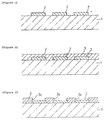
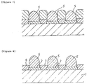
- FIGS 1-8 are drawings that show a series of processes to explain the method of forming solder bumps of this invention.
- This board 1 can be a printed board made of resin material or ceramic material.
- a low-temperature-baked board was used.
- a conductor wiring pattern 2 was formed on board 1 by screen printing using copper paste.
- the line-width of the conductor line pattern 2 was 100 ⁇ m, and the pitch was 150 ⁇ m.
- the wiring pattern was 100 ⁇ m
- the pitch was 150 ⁇ m.
- the wiring pattern but also lands (not shown) for discrete parts were formed on the surface of board 1 .
- the liquid first solder resist 3 was formed on the surface of the board 1 on which the wiring pattern 2 had been formed.
- This solder resist 3 is a photosensitive solder resist and can be obtained by mixing, for example, a commercially available photosensitive solder resist in a base resin/curing agent ratio of 4:1.
- the first solder resist 3 was full-surface printed by ordinary screen printing, following which it was dried at 75°C for .25 minutes.
- the first solder resist was 15 ⁇ m thick.
- the first openings were formed by photoetching at the sites of the first solder resist 3 where the solder bumps were to be formed.
- the first solder resist 3 was exposed using a photomask.
- the exposure conditions were irradiation with a light energy of 800 mJ/cm2 by a 500-W ultrahigh pressure mercury vapor lamp, shielding only the areas where the solder bumps were to be formed, and curing the areas other than this.
- the solder-bump-forming regions were rectangles of the dimensions 200 ⁇ 100 ⁇ m (extending 200 ⁇ m in the line direction).
- the second solder resist 4 was formed on the board shown in Figure 3 [sic; 4?].
- a 38- ⁇ m thick photosensitive dry film in sheet form was used as the second solder resist.
- This second solder resist 4 was laminated on the first solder resist 3 using a laminator. In this instance, gaps formed in the parts at the first openings 3a , but these parts were removed later, so they were not a problem. Second openings were formed in this sheet-like second solder resist 4 by photoetching. The photomask used in forming the first openings was used at this time.
- solder paste was supplied to the first and second openings by printing using a 0.03 mm-thick metal mask.
- Solder 5 can also be filled in the openings directly with a squeegee without the use of a metal mask.
- the substrate was immersed in a 2% aqueous sodium hydroxide solution for 5 minutes to remove only the second solder resist. At this time, etching was performed so that at least part of the first solder resist remained.
- a 2% aqueous sodium hydroxide solution is used as the etchant, the etching rate of the dry film is fast, but the etching rate of the first solder resist material is extremely slow, so the solder bumps shown in Figure 8 were obtained in this way.
- the residues of flux and solder produced during solder coating can be removed, and durability, and reliability can be improved.
- the amount of solder necessary to connect ICs can be obtained just by appropriately establishing the thicknesses of the first solder resist 3 and second solder resist 4 , especially that of the sheet-like second solder resist.
- Figure 9 is a diagrammatic cross section that shows a modification of the method of forming solder bumps of this invention.
- the first solder resist 3 was made relatively thick, but here the first solder resist material was coated so that the liquid solder resist fills the spaces in the wiring pattern 2 as shown in Figure 9(a), the sheet-like second solder resist 4 was laminated on that ( Figure 9(b)), and then openings were formed by photoetching as shown in Figure 9(c).
- the first solder resist material was filled in the spaces between the lines, the second solder resist 4 was formed over the wiring pattern, and then openings 4a were formed by photoetching at the sites where the solder bumps were to be formed as shown in Figure 9(c).
- both the first and second solder resist materials can be cured by one exposure process, with the result that one photoetching process can be eliminated.
- the solder bumps were subsequently formed via a solder supply process and a reflow process.
- Figures 10 through 18 are diagrammatic cross sections showing another modification of the method of forming solder bumps of this invention. This example explains a method of forming solder bumps that can be further miniaturized. The same structural elements as in the examples described above are explained using the same symbols.
- Figure 10 is a diagrammatic plan view showing the configuration immediately before filling in the solder. In this example, the solder bumps were formed in a zigzag pattern.
- Figures 11 through 17 are a series of process drawings in which the board is viewed from line II-II in Figure 10.
- the first solder resist 3 was coated on a board 1 on which conductor lines 2a through 2c had been formed, so as to fill the spaces between conductor lines 2a-2c .
- a liquid photosensitive polyimide resin was used as the first solder resist 3 , and this was dried.
- second openings having an opening area of S2 that were round and connected with the first openings were formed by photoetching at the sites where the solder bumps were to be formed.
- a 1% aqueous sodium carbonate solution was used as the developer.
- This 1% aqueous sodium carbonate solution had a high etching effect on the dry film 10 , but hardly any etching effect on the polyimide resin. Therefore, the second solder resist 3 on the lower side remained as before, without being etched.
- openings of the configuration shown in 15 were formed. These were formed so that the area ratio of the first and second openings, S2/S1, was S2/S1 > 1 , preferably S2/S1 > 2 .
- the openings were filled with solder 6 .
- the second openings had a larger opening area, so even though the opening area of the first openings was small, a large amount of solder could be fed into those openings.
- solder bumps shown in Figure 18 could be obtained.
- the individual conductor lines are completely insulated from each other by polyimide resin, so problems such as shorting do not arise. Also, bumps of sufficient height and sufficient amount of solder are formed, so even if further miniaturized, highly reliable bumps of excellent durability can be formed.
- solder resist materials can be used.
- a photosensitive solder resist can be coated so as to fill the spaces between conductor lines, and after that has dried, the same photosensitive solder resist material can be formed as the first resist layer and a dry film laminated over that.
- a combination of liquid photosensitive polyimide, liquid photosensitive polyimide, and dry film can also be used.
- photosensitive polyimide can be coated, a photosensitive photoresist layer formed over that, and a dry film laminated on that.
- a first solder resist is formed on a board on which conductor wiring has been formed, openings for forming bumps are formed, a second solder resist is formed on top of the first one, openings are again formed, solder is supplied, reflow treatment is carried out, and then the second solder resist is removed. Therefore, even if the conductor wiring is miniaturized, solder bumps of the desired amount of solder can be formed, and the contamination can also be removed. As a result, solder bumps of excellent reliability even if miniaturized can be formed.
Landscapes
- Engineering & Computer Science (AREA)
- Manufacturing & Machinery (AREA)
- Microelectronics & Electronic Packaging (AREA)
- Electric Connection Of Electric Components To Printed Circuits (AREA)
- Wire Bonding (AREA)
- Non-Metallic Protective Coatings For Printed Circuits (AREA)
- Manufacturing Of Printed Wiring (AREA)
Applications Claiming Priority (2)
| Application Number | Priority Date | Filing Date | Title |
|---|---|---|---|
| JP63682/94 | 1994-03-31 | ||
| JP6063682A JPH07273439A (ja) | 1994-03-31 | 1994-03-31 | 半田バンプ形成方法 |
Publications (2)
| Publication Number | Publication Date |
|---|---|
| EP0675532A2 true EP0675532A2 (fr) | 1995-10-04 |
| EP0675532A3 EP0675532A3 (fr) | 1996-04-17 |
Family
ID=13236391
Family Applications (1)
| Application Number | Title | Priority Date | Filing Date |
|---|---|---|---|
| EP95104788A Withdrawn EP0675532A3 (fr) | 1994-03-31 | 1995-03-31 | Procédé de formation des bosses de soudure sur une plaque de montage pour IC. |
Country Status (4)
| Country | Link |
|---|---|
| EP (1) | EP0675532A3 (fr) |
| JP (1) | JPH07273439A (fr) |
| KR (1) | KR950028585A (fr) |
| CN (1) | CN1128486A (fr) |
Cited By (7)
| Publication number | Priority date | Publication date | Assignee | Title |
|---|---|---|---|---|
| US5689049A (en) * | 1994-12-08 | 1997-11-18 | Pioneer Hi-Bred International, Inc. | Transgenic plant and method for producing male sterility using anther specific promoter 5126 |
| EP0849983A1 (fr) * | 1996-12-20 | 1998-06-24 | Alcatel | Procédé pour la réalisation de dispositifs d'écartement dans un circuit imprimé |
| WO2007078716A1 (fr) * | 2005-12-29 | 2007-07-12 | Intel Corporation | Procédé pour la réalisation avancée de perles de soudures et systèmes fabriqués par ledit procédé |
| US7585541B2 (en) * | 1996-12-19 | 2009-09-08 | Ibiden Co., Ltd. | Printed wiring board and method for manufacturing the same |
| WO2009130442A1 (fr) * | 2008-04-24 | 2009-10-29 | The Welding Institute | Procédé permettant d’appliquer une bosse sur un substrat |
| CN102458039A (zh) * | 2010-10-18 | 2012-05-16 | 上海嘉捷通电路科技有限公司 | 一种厚铜线路板 |
| CN113923885A (zh) * | 2021-09-18 | 2022-01-11 | 厦门大学 | 用于焊接微小芯片的柔性线路板的制作方法 |
Families Citing this family (13)
| Publication number | Priority date | Publication date | Assignee | Title |
|---|---|---|---|---|
| JP3500032B2 (ja) * | 1997-03-13 | 2004-02-23 | 日本特殊陶業株式会社 | 配線基板及びその製造方法 |
| WO2000010369A1 (fr) | 1998-08-10 | 2000-02-24 | Fujitsu Limited | Realisation de bossages de soudure, methode de montage d'un dispositif electronique et structure de montage pour ce dispositif |
| JP3423930B2 (ja) * | 1999-12-27 | 2003-07-07 | 富士通株式会社 | バンプ形成方法、電子部品、および半田ペースト |
| JP4748889B2 (ja) * | 2000-12-26 | 2011-08-17 | イビデン株式会社 | 多層プリント配線板の製造方法 |
| JP4707273B2 (ja) * | 2000-12-26 | 2011-06-22 | イビデン株式会社 | 多層プリント配線板の製造方法 |
| JP4212992B2 (ja) * | 2003-09-03 | 2009-01-21 | Tdk株式会社 | 半田ボールの供給方法および供給装置 |
| JP2006135156A (ja) * | 2004-11-08 | 2006-05-25 | Compeq Manufacturing Co Ltd | 回路基板上へのはんだバンプの形成方法 |
| TWI253888B (en) | 2004-12-09 | 2006-04-21 | Advanced Semiconductor Eng | Method of packaging flip chip and method of forming pre-solders on substrate thereof |
| JP4669703B2 (ja) * | 2005-01-19 | 2011-04-13 | イビデン株式会社 | プリント配線板及びその製法 |
| JP2010245317A (ja) * | 2009-04-07 | 2010-10-28 | Ricoh Microelectronics Co Ltd | 電子部品実装方法 |
| JP2013506298A (ja) * | 2009-09-23 | 2013-02-21 | スリーエム イノベイティブ プロパティズ カンパニー | 電気的接続部及びその製造法 |
| JP5585354B2 (ja) * | 2010-09-29 | 2014-09-10 | 凸版印刷株式会社 | 半導体パッケージの製造方法 |
| CN110676175A (zh) * | 2019-09-24 | 2020-01-10 | 浙江集迈科微电子有限公司 | 一种键合工艺制作大锡球的方法 |
Family Cites Families (3)
| Publication number | Priority date | Publication date | Assignee | Title |
|---|---|---|---|---|
| JPS57152146A (en) * | 1981-03-13 | 1982-09-20 | Citizen Watch Co Ltd | Manufacture of semiconductor device |
| JPH0252436A (ja) * | 1988-08-17 | 1990-02-22 | Shimadzu Corp | ハンダバンプ製造方法 |
| US5316788A (en) * | 1991-07-26 | 1994-05-31 | International Business Machines Corporation | Applying solder to high density substrates |
-
1994
- 1994-03-31 JP JP6063682A patent/JPH07273439A/ja not_active Withdrawn
-
1995
- 1995-03-31 KR KR1019950007230A patent/KR950028585A/ko not_active Ceased
- 1995-03-31 EP EP95104788A patent/EP0675532A3/fr not_active Withdrawn
- 1995-03-31 CN CN95104538A patent/CN1128486A/zh active Pending
Cited By (14)
| Publication number | Priority date | Publication date | Assignee | Title |
|---|---|---|---|---|
| US5689049A (en) * | 1994-12-08 | 1997-11-18 | Pioneer Hi-Bred International, Inc. | Transgenic plant and method for producing male sterility using anther specific promoter 5126 |
| US7615162B2 (en) | 1996-12-19 | 2009-11-10 | Ibiden Co., Ltd. | Printed wiring board and method for manufacturing the same |
| USRE43509E1 (en) | 1996-12-19 | 2012-07-17 | Ibiden Co., Ltd. | Printed wiring board and method for manufacturing the same |
| US7585541B2 (en) * | 1996-12-19 | 2009-09-08 | Ibiden Co., Ltd. | Printed wiring board and method for manufacturing the same |
| US7712212B2 (en) | 1996-12-19 | 2010-05-11 | Ibiden Co., Ltd. | Method for manufacturing printed wiring board |
| EP0849983A1 (fr) * | 1996-12-20 | 1998-06-24 | Alcatel | Procédé pour la réalisation de dispositifs d'écartement dans un circuit imprimé |
| US6036836A (en) * | 1996-12-20 | 2000-03-14 | Peeters; Joris Antonia Franciscus | Process to create metallic stand-offs on an electronic circuit |
| US7790598B2 (en) | 2005-12-29 | 2010-09-07 | Intel Corporation | System, apparatus, and method for advanced solder bumping |
| US7517788B2 (en) | 2005-12-29 | 2009-04-14 | Intel Corporation | System, apparatus, and method for advanced solder bumping |
| CN101310374B (zh) * | 2005-12-29 | 2011-12-14 | 英特尔公司 | 用于高级焊料凸点形成的方法 |
| WO2007078716A1 (fr) * | 2005-12-29 | 2007-07-12 | Intel Corporation | Procédé pour la réalisation avancée de perles de soudures et systèmes fabriqués par ledit procédé |
| WO2009130442A1 (fr) * | 2008-04-24 | 2009-10-29 | The Welding Institute | Procédé permettant d’appliquer une bosse sur un substrat |
| CN102458039A (zh) * | 2010-10-18 | 2012-05-16 | 上海嘉捷通电路科技有限公司 | 一种厚铜线路板 |
| CN113923885A (zh) * | 2021-09-18 | 2022-01-11 | 厦门大学 | 用于焊接微小芯片的柔性线路板的制作方法 |
Also Published As
| Publication number | Publication date |
|---|---|
| KR950028585A (ko) | 1995-10-18 |
| CN1128486A (zh) | 1996-08-07 |
| EP0675532A3 (fr) | 1996-04-17 |
| JPH07273439A (ja) | 1995-10-20 |
Similar Documents
| Publication | Publication Date | Title |
|---|---|---|
| EP0675532A2 (fr) | Procédé de formation des bosses de soudure sur une plaque de montage pour IC | |
| KR100295732B1 (ko) | 인쇄배선기판홀충진방법 | |
| US4985601A (en) | Circuit boards with recessed traces | |
| US8299368B2 (en) | Interconnection element for electric circuits | |
| US9485853B2 (en) | Wiring substrate having a plurality of connection terminals and a filling member provided therebetween | |
| EP2874477B1 (fr) | Carte de câblage | |
| US20080017410A1 (en) | Method for forming a plated microvia interconnect | |
| US20140097007A1 (en) | Wiring substrate and method for producing the same | |
| US9824977B2 (en) | Semiconductor packages and methods of forming the same | |
| KR100225655B1 (ko) | 반도체 패키지의 인쇄회로기판 실장 구조 | |
| EP2927950B1 (fr) | Carte de câblage | |
| JP2006032947A (ja) | 高密度基板の製造方法 | |
| US5525204A (en) | Method for fabricating a printed circuit for DCA semiconductor chips | |
| KR102310979B1 (ko) | 제한된 솔더 상호 연결 패드들을 가진 회로 보드 및 그 제조 방법 | |
| JPH09232741A (ja) | プリント配線板 | |
| US6210746B1 (en) | Method of fabricating a solder resist mask | |
| JP2725665B2 (ja) | プリント配線板製造方法 | |
| JPH10209612A (ja) | 回路基板およびその製造方法 | |
| JP2000307217A (ja) | 配線パターンの形成方法及び半導体装置 | |
| JP3224056B2 (ja) | バンプを備えた可撓性回路基板及びその製造法 | |
| JPH10242629A (ja) | プリント配線板及びその製造方法 | |
| JPH0567871A (ja) | 印刷配線板及びその製造方法 | |
| JP2000307224A (ja) | はんだボール対策用プリント配線板 | |
| JPH05259622A (ja) | プリント配線板 | |
| JP2004221387A (ja) | プリント配線板における電子部品実装方法 |
Legal Events
| Date | Code | Title | Description |
|---|---|---|---|
| PUAI | Public reference made under article 153(3) epc to a published international application that has entered the european phase |
Free format text: ORIGINAL CODE: 0009012 |
|
| AK | Designated contracting states |
Kind code of ref document: A2 Designated state(s): DE FR GB |
|
| PUAL | Search report despatched |
Free format text: ORIGINAL CODE: 0009013 |
|
| AK | Designated contracting states |
Kind code of ref document: A3 Designated state(s): DE FR GB |
|
| 17P | Request for examination filed |
Effective date: 19960820 |
|
| 17Q | First examination report despatched |
Effective date: 19961218 |
|
| STAA | Information on the status of an ep patent application or granted ep patent |
Free format text: STATUS: THE APPLICATION HAS BEEN WITHDRAWN |
|
| 18W | Application withdrawn |
Withdrawal date: 19970610 |