EP0675561A1 - Procédé de fabrication d'un circulateur hyperfréquence - Google Patents
Procédé de fabrication d'un circulateur hyperfréquence Download PDFInfo
- Publication number
- EP0675561A1 EP0675561A1 EP95400698A EP95400698A EP0675561A1 EP 0675561 A1 EP0675561 A1 EP 0675561A1 EP 95400698 A EP95400698 A EP 95400698A EP 95400698 A EP95400698 A EP 95400698A EP 0675561 A1 EP0675561 A1 EP 0675561A1
- Authority
- EP
- European Patent Office
- Prior art keywords
- ferromagnetic material
- inner conductors
- circulator
- insulating
- insulating ferromagnetic
- Prior art date
- Legal status (The legal status is an assumption and is not a legal conclusion. Google has not performed a legal analysis and makes no representation as to the accuracy of the status listed.)
- Granted
Links
- 238000004519 manufacturing process Methods 0.000 title claims abstract description 13
- 239000004020 conductor Substances 0.000 claims abstract description 80
- 239000003302 ferromagnetic material Substances 0.000 claims abstract description 75
- 238000010304 firing Methods 0.000 claims abstract description 20
- 230000005294 ferromagnetic effect Effects 0.000 claims abstract description 16
- 238000005245 sintering Methods 0.000 claims abstract description 11
- 238000010030 laminating Methods 0.000 claims abstract description 9
- 239000000463 material Substances 0.000 claims abstract description 7
- 230000005291 magnetic effect Effects 0.000 claims description 28
- 238000000034 method Methods 0.000 claims description 24
- 229910052751 metal Inorganic materials 0.000 claims description 14
- 239000002184 metal Substances 0.000 claims description 14
- 239000003990 capacitor Substances 0.000 claims description 11
- 230000005284 excitation Effects 0.000 claims description 4
- 230000035699 permeability Effects 0.000 description 10
- 239000000758 substrate Substances 0.000 description 10
- 230000004907 flux Effects 0.000 description 8
- 239000000696 magnetic material Substances 0.000 description 7
- 230000008569 process Effects 0.000 description 7
- 238000002347 injection Methods 0.000 description 6
- 239000007924 injection Substances 0.000 description 6
- 238000003780 insertion Methods 0.000 description 6
- 230000037431 insertion Effects 0.000 description 6
- 230000001902 propagating effect Effects 0.000 description 5
- OKTJSMMVPCPJKN-UHFFFAOYSA-N Carbon Chemical compound [C] OKTJSMMVPCPJKN-UHFFFAOYSA-N 0.000 description 4
- KDLHZDBZIXYQEI-UHFFFAOYSA-N Palladium Chemical compound [Pd] KDLHZDBZIXYQEI-UHFFFAOYSA-N 0.000 description 4
- BQCADISMDOOEFD-UHFFFAOYSA-N Silver Chemical compound [Ag] BQCADISMDOOEFD-UHFFFAOYSA-N 0.000 description 4
- 229910052799 carbon Inorganic materials 0.000 description 4
- 239000002904 solvent Substances 0.000 description 4
- 239000011230 binding agent Substances 0.000 description 3
- 238000002844 melting Methods 0.000 description 3
- 230000008018 melting Effects 0.000 description 3
- 239000007769 metal material Substances 0.000 description 3
- 238000010295 mobile communication Methods 0.000 description 3
- 238000007639 printing Methods 0.000 description 3
- 229910052709 silver Inorganic materials 0.000 description 3
- 239000004332 silver Substances 0.000 description 3
- QTBSBXVTEAMEQO-UHFFFAOYSA-N Acetic acid Natural products CC(O)=O QTBSBXVTEAMEQO-UHFFFAOYSA-N 0.000 description 2
- 239000004593 Epoxy Substances 0.000 description 2
- UFWIBTONFRDIAS-UHFFFAOYSA-N Naphthalene Chemical compound C1=CC=CC2=CC=CC=C21 UFWIBTONFRDIAS-UHFFFAOYSA-N 0.000 description 2
- PXHVJJICTQNCMI-UHFFFAOYSA-N Nickel Chemical compound [Ni] PXHVJJICTQNCMI-UHFFFAOYSA-N 0.000 description 2
- 229910052763 palladium Inorganic materials 0.000 description 2
- 238000000926 separation method Methods 0.000 description 2
- 238000005476 soldering Methods 0.000 description 2
- DSSYKIVIOFKYAU-XCBNKYQSSA-N (R)-camphor Chemical compound C1C[C@@]2(C)C(=O)C[C@@H]1C2(C)C DSSYKIVIOFKYAU-XCBNKYQSSA-N 0.000 description 1
- VYZAMTAEIAYCRO-UHFFFAOYSA-N Chromium Chemical compound [Cr] VYZAMTAEIAYCRO-UHFFFAOYSA-N 0.000 description 1
- 241000723346 Cinnamomum camphora Species 0.000 description 1
- RYGMFSIKBFXOCR-UHFFFAOYSA-N Copper Chemical compound [Cu] RYGMFSIKBFXOCR-UHFFFAOYSA-N 0.000 description 1
- -1 acetic acid compound Chemical class 0.000 description 1
- 238000005452 bending Methods 0.000 description 1
- 230000005540 biological transmission Effects 0.000 description 1
- 229960000846 camphor Drugs 0.000 description 1
- 229930008380 camphor Natural products 0.000 description 1
- 239000000919 ceramic Substances 0.000 description 1
- 229910052804 chromium Inorganic materials 0.000 description 1
- 239000011651 chromium Substances 0.000 description 1
- 229910052802 copper Inorganic materials 0.000 description 1
- 239000010949 copper Substances 0.000 description 1
- 239000006071 cream Substances 0.000 description 1
- 239000002223 garnet Substances 0.000 description 1
- 239000011521 glass Substances 0.000 description 1
- 239000011810 insulating material Substances 0.000 description 1
- MTRJKZUDDJZTLA-UHFFFAOYSA-N iron yttrium Chemical compound [Fe].[Y] MTRJKZUDDJZTLA-UHFFFAOYSA-N 0.000 description 1
- 238000000465 moulding Methods 0.000 description 1
- 229910052759 nickel Inorganic materials 0.000 description 1
- 239000000843 powder Substances 0.000 description 1
- 230000009467 reduction Effects 0.000 description 1
- 229910000679 solder Inorganic materials 0.000 description 1
- 239000006104 solid solution Substances 0.000 description 1
Images


Classifications
-
- H—ELECTRICITY
- H01—ELECTRIC ELEMENTS
- H01P—WAVEGUIDES; RESONATORS, LINES, OR OTHER DEVICES OF THE WAVEGUIDE TYPE
- H01P11/00—Apparatus or processes specially adapted for manufacturing waveguides or resonators, lines, or other devices of the waveguide type
-
- H—ELECTRICITY
- H01—ELECTRIC ELEMENTS
- H01P—WAVEGUIDES; RESONATORS, LINES, OR OTHER DEVICES OF THE WAVEGUIDE TYPE
- H01P1/00—Auxiliary devices
- H01P1/32—Non-reciprocal transmission devices
- H01P1/38—Circulators
- H01P1/383—Junction circulators, e.g. Y-circulators
- H01P1/387—Strip line circulators
Definitions
- the present invention relates to a method of manufacturing a circulator used in a microwave band radio device, for example in a mobile communication device such as a portable telephone.
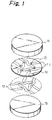
- a conventional lumped element type circulator has an assembled circulator element with a circular plane shape and a basic structure as shown in an exploded oblique view of Fig. 1.
- a reference numeral 10 denotes a circular substrate made of a non-magnetic material such as a glass-reinforced epoxy.
- Coil conductors (inner conductors) 11 and 12 are formed on top and bottom surfaces of the non-magnetic material substrate 10, respectively. These coil conductors 11 and 12 are electrically connected with each other by via holes 13 passing through the substrate 10.
- Circularly shaped members 14 and 15 made of a ferromagnetic material are attached to the both surfaces of the non-magnetic material substrate 10 having the coil conductors 11 and 12 so that rotating RF (Radio Frequency) magnetic fluxes are induced in these ferromagnetic members 14 and 15 due to an RF power applied to the coil conductors 11 and 12.
- the conventional circulator element in the circulator has a circular plane shape and is constructed by assembling, namely piling and bonding, the ferromagnetic members 14 and 15 on the both sides of the non-magnetic material substrate 10.
- the circulator is then constructed, as shown in its exploded oblique view of Fig. 2, by stacking and fixing in sequence grounding conductor electrodes 16 and 17, exiting permanent magnets 18 and 19 and a metal housing separated to upper and lower parts 20 and 21 on the both ferromagnetic members 14 and 15, respectively.
- the housing parts 20 and 21 form a magnetic path of the magnetic flux from and to the exiting permanent magnets 18 and 19.
- the circulator may have resonating capacitors for resonating its input frequency and terminal circuits for connecting the circulator with the external circuits.
- the circulator element and the resonating capacitors may be formed in integral, and an impedance transducer for broadening the operating frequency of the circulator may be provided in the terminal circuits.
- RF magnetic flux rotating around the coil conductors 11 and 12 will be produced in the ferromagnetic members 14 and 15.
- a dc magnetic field perpendicular to the RF magnetic flux is applied from the permanent magnets 18 and 19, the ferromagnetic members 14 and 15 present different permeability ⁇ + and ⁇ depending upon rotating sense of the RF magnetic flux, as shown in Fig. 3.
- a circulator utilizes this difference of the permeability depending upon the rotating sense.
- a propagation velocity of the RF signal in the circulator element will differ in accordance with the rotating sense and thus the signals transmitting to the opposite directions will be canceled each other resulting that the propagation of the signal to a particular port is prevented.
- a non-propagating port is determined in accordance with its angle against a driving port due to the permeability ⁇ + and ⁇ of the ferromagnetic member. For example, if ports A, B and C are arranged in this order along a certain rotating sense, the port B will be determined as the non-propagating port against the driving port A and the port C will be determined as the non-propagating port against the driving port B.
- the circulators have been broadly utilized as effective elements for preventing interference between amplifiers in a mobile communication device such as a portable telephone and also for protecting a power amplifier in the mobile communication device from a reflected power.
- the circulators With the spread of and downsizing of recent radio transmission devices, the circulators themselves are requested to be manufactured in lower cost and in smaller size and to operate with lower loss and in broader frequency band. In order to satisfy these requirements, it will be necessary to make a circulator having a large difference between the permeability ⁇ + and ⁇ and having a driving circuit with small loss.
- Another object of the present invention is to provide a manufacturing method which can make a circulator in a lower cost.
- Further object of the present invention is to provide a manufacturing method which can make a circulator capable of operating in a broader frequency range.
- Still further object of the present invention is to provide a manufacturing method which can make a circulator capable of operating with lower loss.
- a method of manufacturing a circulator includes the steps of forming, on at least one sheet of an insulating ferromagnetic material, dummy inner conductors made of a material which is thermally decomposed at a temperature equal to or less than a sintering completion temperature of the insulating ferromagnetic material, laminating a plurality of the sheets of the insulating ferromagnetic material so that at least one insulating ferromagnetic material sheet covers the dummy inner conductors formed on the insulating ferromagnetic material sheet, firing the laminated insulating ferromagnetic material sheets to form an insulating ferromagnetic material body in a single continuous body and to form ducts for inner conductors at portions occupied by the dummy inner conductors, injecting with pressure conductive paste into the ducts in the insulating ferromagnetic material body, and firing the insulating ferromagnetic material body to form the inner conductors in the insulating ferromagnetic material
- the conductive metal material paste is injected with pressure into the ducts prepared for the inner conductors after firing and sintering the ferromagnetic material body. Therefore, even if a metal such as silver, which has a melting point lower than a sintering completion temperature of the ferromagnetic material, is used for the inner conductors, the metal material will never be vapored during the sintering process of the ferromagnetic material body. Thus, the volume of the inner conductor will not reduce preventing poor characteristics of the circulator due to increasing of its loss or its breakage from occurring. As a result, a circulator with low resistance inner conductors, and thus with low insertion loss can be provided.
- the insulating ferromagnetic material body for closely surrounding the inner conductors is sintered into a single continuous body, there is no discontinuous portion in this ferromagnetic material body.
- the RF magnetic flux will close in the circulator element resulting that no demagnetizing field will be produced and thus the difference between the permeability ⁇ + and ⁇ will become large.
- broader operating frequency range and lower loss can be obtained with a smaller size circulator.
- the method further includes a step of forming, on side surfaces of the insulating ferromagnetic material body, a plurality of terminal electrodes so as to be electrically connected to respective ends of the inner conductors, and a step of electrically connecting circuit elements to the terminal electrodes, respectively.
- the connecting step may preferably include a step of electrically connecting resonating capacitors to the terminal electrodes, respectively.
- the method further includes a step of attaching, on upper side and lower side of the insulating ferromagnetic body, excitation permanent magnets for applying a dc magnetic field to the insulating ferromagnetic material body, respectively.
- the method further may include a step of closely fixing a metal housing having a continuous magnetic path to the excitation permanent magnets. Since the exciting magnetic path is continuous, a smaller magnetic resistance can be obtained causing its characteristics to extremely improve.
- the laminating step includes a step of laminating an upper ferromagnetic material layer, at least one intermediate ferromagnetic material layer and a lower ferromagnetic material layer in this order, and wherein the dummy inner conductors forming step includes a step of forming dummy inner conductors on top surfaces of the intermediate ferromagnetic material layer and the lower ferromagnetic material layer.
- the method may further include a step of forming grounding conductors on a top surface of the upper ferromagnetic material layer and a bottom surface of the lower ferromagnetic material layer, respectively, and a step of forming conductors connecting the two grounding conductors with each other provided on a side surface of the insulating ferromagnetic material body.
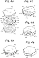
- Figs. 4a to 4e schematically show parts of manufacturing processes of a circulator element of a three-port circulator as a preferred embodiment according to the present invention
- Fig. 5 shows the circulator element with permanent magnets and capacitors.
- the circulator manufactured by this embodiment is a three-port circulator and its circulator element is formed with a plane shape of a regular hexagon.
- the plane shape of this element may be formed in any hexagonal shape or another polygonal shape so far as a symmetrical rotating magnetic field can be produced. Thanks for the polygonal plane shape of the circulator element, spaces for attaching discrete circuit elements such as resonating capacitors or termination resisters will remain on side surfaces of the circulator element. Therefore, if such the discrete circuit elements are additionally attached to the circulator element, a total size of the circulator can be maintained in small.
- an upper ferromagnetic material sheet 40 having a thickness of about 1 mm, an intermediate ferromagnetic material sheet 41 having a thickness of about 160 ⁇ m and a lower ferromagnetic material sheet 42 having a thickness of about 1 mm are prepared.
- the upper and lower ferromagnetic material sheets 40 and 42 may be formed by laminating a plurality of green sheets with a thickness in general of 100 to 200 ⁇ m (preferably 160 ⁇ ). These ferromagnetic material sheets are made of the same insulating ferromagnetic material.
- This ferromagnetic material may be yttrium iron garnet (hereinafter called as YIG) and the ferromagnetic material sheets will be made of YIG, a binder and a solvent with the following ratio of components.
- Via holes 43a, 43b and 43c passing through the intermediate sheet 41 are formed at predetermined positions of this sheet 41.
- upper dummy inner conductors 44a, 44b and 44c made of carbon paste and lower dummy inner conductors 45a, 45b and 45c made of carbon paste are formed by printing or transferring them.
- These dummy inner conductors made of the carbon paste, used in order to form upper inner conductor ducts and lower inner conductor ducts by firing, may be made of any kind of paste such as acetic acid compound paste, or naphthalene or camphor paste which will be easily sublimated other than the carbon paste in condition that the paste can be thermally decomposed without expansion at a temperature less than a sintering completion temperature of the ferromagnetic material.
- these dummy inner conductors 44a, 44b and 44c are formed in three pairs of strip patterns. Each pair of strip patterns extends to the same radiating direction (a direction perpendicular to at least one side of the hexagon) by stepping aside from the via holes of another strip pattern.
- These dummy inner conductors may be formed in any optional patterns with a trigonally symmetric coil pattern for the three-port circulator.
- these dummy inner conductors may be formed in a pattern with a single or a plurality of straight strip patterns, a pattern combining the straight strip patterns with the above-mentioned trigonally symmetric patterns or a pattern with no via hole.
- Fig. 4a illustrates that each of sheets to be stacked has been already diced and separated to the respective circulator elements, these sheets are in practice diced and separated after stacking the sheets with the printed dummy inner conductors.
- the circulator elements formed by separating the stacked sheets are then fired at a temperature of such as 1450 °C for example, which is equal to or higher than a sintering completion temperature of the YIG.
- This firing process may be carried out one time or more than one time. If a plurality of firing processes are carried out, at least one of the firing must be executed at a temperature equal to or higher than the sintering completion temperature of the YIG.
- the ferromagnetic material layers constituting the upper sheet 40, intermediate sheet 41 and lower sheet 43 are integrally formed into a single continuous body 46 as shown in Fig. 4c.
- the paste which has constituted the dummy inner conductors thermally decomposes and escapes in vapor so that ducts 47 for inner conductors are formed at the portions where the dummy inner conductors were occupied, within the ferromagnetic material body 46.
- respective ends 47a, 47b and 47c of the ducts 47 are opened. Furthermore, the portions of the via holes 43a, 43b and 43c passing through the intermediate sheet 41 will remain as vacancies within the body 46.
- firing is performed after the stacked sheets are diced and separated.
- this firing process can be effected before the dicing and separation process if the stacked sheets have an escape opening for passing vapor of the thermally decomposed paste.
- upper inner conductors 48, lower inner conductors and via hole conductors are formed in the ferromagnetic body 46, and also one ends of the upper inner conductors 48 are electrically connected to one ends of the lower inner conductors through the via hole conductors, respectively.
- the inner conductors with a trigonally symmetric coil pattern for the three-port circulator are formed in the ferromagnetic material body 16 so that propagation characteristics among the ports of the three-port circulator will be identical with each other.
- terminal electrodes 49 are formed by baking on every other side surfaces of the ferromagnetic material body 46, respectively, and grounding conductors 50 are formed on a top surface and a bottom surface and also on the remaining side surfaces of the body 46 by baking.
- the other ends of the upper inner conductors, which are appeared on the side surfaces of the body 46. are electrically connected to the terminal electrodes (49), respectively.
- the other ends of the lower inner conductors, which are appeared on the side surfaces of the circulator element are electrically connected to the grounding conductors (50).
- These terminal electrodes and the grounding conductors can be formed by printing the conductive paste and then by firing the printed paste simultaneously with the aforementioned firing of the injected conductive paste for the inner conductors.
- the circulator element thus manufactured has a plane shape in a regular hexagon inscribed in a circle with 4 mm diameter and has a thickness of 1 mm.
- Resonating capacitors 51a, 51b and 51c may be mounted and soldered by a reflow soldering to the terminal electrodes (49) of the circulator element, respectively, as shown in Fig. 5.
- a circulator is then finished by assembling exciting permanent magnets 52 and 53 for applying a dc magnetic field and a metal housing operating also as a magnetic yoke, with the circulator element.
- Figs. 6a, 6b and 6c illustrate a structure of a housing and a structure of the circulator with the circulator element and exciting permanent magnets assembled in the housing.
- the exciting permanent magnets 62 and 63 are stacked respectively on and under the circulator element 60 which has the resonating capacitors 61a attached to its side surfaces.
- the stacked body of the circulator element 60 and the permanent magnets 62 and 63 are sandwiched and supported between support members 64 and 65 made of an insulating material as shown in Fig. 6b.
- connection leads 67a with cream solder are mechanically caught between input/output terminals 66a formed in the insulating support members 64 and 65 and the resonating capacitors 61a attached to the circulator element 60 or terminal electrodes formed on the side surfaces of the circulator element 60, respectively.
- the connection lead 67a may be constituted by a U-turned elastic thin strip of copper for example.
- the insulating support member 64 (65) is formed by molding ceramic, glass reinforced epoxy or another plastic material capable of resisting to high temperature.
- the assembly 68 constituted by the stacked body and the insulating support members 64 and 65 is closely inserted into a metal housing 69 and fixed in the housing 69 by bending projected tongue portions 70.
- the metal housing 69 and the permanent magnets 62 and 63 are closely contacted with each other.
- the metal housing 69 is made of a metal capable of operating as a magnetic yoke and the surface of the housing is plated by nickel or chromium.
- the metal housing 69 itself has substantially a square drum shape with integrally surrounding four faces and opened two opposite faces.
- connection leads 67a are electrically connected to the input/output terminals 66a and to the resonating capacitors 61a or the terminal electrodes, respectively.
- Fig. 6c shows the finished circulator 71.
- Operating frequency range and loss of the circulator is mainly determined by the performance of its circulator element. Larger difference between the permeability ⁇ + and ⁇ and also lower coil resistance and lower magnetic loss tangent will result broader operating frequency range and lower loss of the circulator element.
- the circulator according to this embodiment using the inner conductor pressure-injection method can obtain following advantages.
- Fig. 7 illustrates insertion loss characteristics of the circulator manufactured by the embodiment shown in Figs. 4a to 4e and the conventional circulator having the same size as that of the former one.
- the axis of abscissa indicates frequency and the axis of ordinate indicates an insertion loss between non-propagating ports and an insertion loss between propagating ports. It is apparent from this figure that the circulator according to the embodiment of Figs. 4a to 4e (the inner conductor pressure-injection method is used) has lower center operating frequency and lower loss than the conventional circulator.
- the ferromagnetic material is made of YIG in the aforementioned embodiments, any insulating ferromagnetic material other than YIG may be used in condition that no solid solution will occur with the inner conductor material.
- the present invention can be applied to a circulator having ports more than three.
- the present invention can be applied to a distributed element circulator having a circulator element integral with a capacitor circuit and having an impedance transformer for broadening the operating frequency band combined in its terminal circuits, other than the lumped element circulator.
- a non-reciprocal circuit element such as an isolator can be easily formed from any of circulators according to the present invention.
Landscapes
- Engineering & Computer Science (AREA)
- Manufacturing & Machinery (AREA)
- Non-Reversible Transmitting Devices (AREA)
Applications Claiming Priority (3)
| Application Number | Priority Date | Filing Date | Title |
|---|---|---|---|
| JP8526594 | 1994-04-01 | ||
| JP6085265A JPH07273507A (ja) | 1994-04-01 | 1994-04-01 | サーキュレータの製造方法 |
| JP85265/94 | 1994-04-01 |
Publications (2)
| Publication Number | Publication Date |
|---|---|
| EP0675561A1 true EP0675561A1 (fr) | 1995-10-04 |
| EP0675561B1 EP0675561B1 (fr) | 2000-06-07 |
Family
ID=13853755
Family Applications (1)
| Application Number | Title | Priority Date | Filing Date |
|---|---|---|---|
| EP95400698A Expired - Lifetime EP0675561B1 (fr) | 1994-04-01 | 1995-03-29 | Procédé de fabrication d'un circulateur hyperfréquence |
Country Status (5)
| Country | Link |
|---|---|
| US (1) | US5611878A (fr) |
| EP (1) | EP0675561B1 (fr) |
| JP (1) | JPH07273507A (fr) |
| CN (1) | CN1038283C (fr) |
| DE (1) | DE69517355T2 (fr) |
Cited By (5)
| Publication number | Priority date | Publication date | Assignee | Title |
|---|---|---|---|---|
| EP0821426A1 (fr) * | 1996-07-26 | 1998-01-28 | Hitachi Metals, Ltd. | Elément de circuit non réciproque |
| EP0800231A3 (fr) * | 1996-04-01 | 2000-02-23 | Honda Giken Kogyo Kabushiki Kaisha | Module d'antenne planaire |
| US6107895A (en) * | 1996-04-03 | 2000-08-22 | Deltec Telesystems International Limited | Circulator and components thereof |
| GB2382472A (en) * | 2001-07-06 | 2003-05-28 | Murata Manufacturing Co | Center electrode assembly, nonreciprocal circuit device, communication device, and method of producing the center electrode assembly |
| WO2004055936A1 (fr) * | 2002-12-17 | 2004-07-01 | Philips Intellectual Property & Standards Gmbh | Element de circuit non reciproque |
Families Citing this family (7)
| Publication number | Priority date | Publication date | Assignee | Title |
|---|---|---|---|---|
| JPH09214209A (ja) * | 1996-02-06 | 1997-08-15 | Murata Mfg Co Ltd | 高周波回路素子およびその製造方法 |
| US6120884A (en) * | 1996-07-26 | 2000-09-19 | Tdk Corporation | Conductor paste and multilayer ceramic part using the same |
| US7942892B2 (en) * | 2003-05-01 | 2011-05-17 | Abbott Cardiovascular Systems Inc. | Radiopaque nitinol embolic protection frame |
| US8217730B1 (en) * | 2011-04-13 | 2012-07-10 | Raytheon Canada Limited | High power waveguide cluster circulator |
| JPWO2016047323A1 (ja) * | 2014-09-25 | 2017-06-15 | 株式会社村田製作所 | フロントエンド回路および通信装置 |
| RU2570228C1 (ru) * | 2014-10-28 | 2015-12-10 | Российская Федерация, от имени которой выступает Государственная корпорация по атомной энергии "Росатом" | Способ изготовления y-сочленения в виде системы переплетённых проводников |
| RU2570665C1 (ru) * | 2014-10-28 | 2015-12-10 | Российская Федерация, от имени которой выступает Государственная корпорация по атомной энергии "Росатом" | Многофункциональное ферритовое развязывающее устройство |
Citations (4)
| Publication number | Priority date | Publication date | Assignee | Title |
|---|---|---|---|---|
| US4618912A (en) * | 1984-08-13 | 1986-10-21 | Murata Manufacturing Co., Ltd. | Monolithic ceramic capacitor |
| US5159294A (en) * | 1990-03-01 | 1992-10-27 | Murata Manufacturing Co., Ltd. | Non-reciprocal circuit element |
| GB2266412A (en) * | 1992-04-17 | 1993-10-27 | Murata Manufacturing Co | Non-reciprocal circuit elements and method thereof |
| GB2269942A (en) * | 1992-08-05 | 1994-02-23 | Murata Manufacturing Co | Non-reciprocal circuit element and method thereof |
Family Cites Families (14)
| Publication number | Priority date | Publication date | Assignee | Title |
|---|---|---|---|---|
| JPS5583301A (en) * | 1978-12-19 | 1980-06-23 | Nec Corp | Isolator |
| JPS5761314A (en) * | 1980-09-05 | 1982-04-13 | Hitachi Metals Ltd | Lumped constant type circulator and isolator |
| JPH01198802A (ja) * | 1987-10-07 | 1989-08-10 | Murata Mfg Co Ltd | 非可逆回路素子 |
| JP3213921B2 (ja) * | 1992-04-25 | 2001-10-02 | 株式会社村田製作所 | 非可逆回路素子 |
| JP3211841B2 (ja) * | 1992-04-17 | 2001-09-25 | 株式会社村田製作所 | 非可逆回路素子およびその製造方法 |
| JPH066112A (ja) * | 1992-06-22 | 1994-01-14 | Fuji Elelctrochem Co Ltd | マイクロ波アイソレータおよびその製造方法 |
| JPH06164222A (ja) * | 1992-11-25 | 1994-06-10 | Murata Mfg Co Ltd | マイクロ波用磁性体及びその製造方法 |
| JP3261779B2 (ja) * | 1993-01-08 | 2002-03-04 | 株式会社村田製作所 | マイクロ波用回路素子 |
| JPH06338707A (ja) * | 1993-03-31 | 1994-12-06 | Tdk Corp | サーキュレータ |
| TW246733B (fr) * | 1993-03-31 | 1995-05-01 | Tdk Electronics Co Ltd | |
| JP3064798B2 (ja) * | 1993-03-31 | 2000-07-12 | ティーディーケイ株式会社 | サーキュレータ及びその製造方法 |
| JPH06291514A (ja) * | 1993-04-02 | 1994-10-18 | Murata Mfg Co Ltd | マイクロ波用非可逆回路素子 |
| JP3178153B2 (ja) * | 1993-04-06 | 2001-06-18 | 株式会社村田製作所 | マイクロ波用非可逆回路素子 |
| JP3147615B2 (ja) * | 1993-10-12 | 2001-03-19 | 株式会社村田製作所 | 高周波用非可逆回路素子 |
-
1994
- 1994-04-01 JP JP6085265A patent/JPH07273507A/ja not_active Withdrawn
-
1995
- 1995-03-21 US US08/407,855 patent/US5611878A/en not_active Expired - Fee Related
- 1995-03-29 EP EP95400698A patent/EP0675561B1/fr not_active Expired - Lifetime
- 1995-03-29 DE DE69517355T patent/DE69517355T2/de not_active Expired - Fee Related
- 1995-03-31 CN CN95104524A patent/CN1038283C/zh not_active Expired - Fee Related
Patent Citations (4)
| Publication number | Priority date | Publication date | Assignee | Title |
|---|---|---|---|---|
| US4618912A (en) * | 1984-08-13 | 1986-10-21 | Murata Manufacturing Co., Ltd. | Monolithic ceramic capacitor |
| US5159294A (en) * | 1990-03-01 | 1992-10-27 | Murata Manufacturing Co., Ltd. | Non-reciprocal circuit element |
| GB2266412A (en) * | 1992-04-17 | 1993-10-27 | Murata Manufacturing Co | Non-reciprocal circuit elements and method thereof |
| GB2269942A (en) * | 1992-08-05 | 1994-02-23 | Murata Manufacturing Co | Non-reciprocal circuit element and method thereof |
Non-Patent Citations (2)
| Title |
|---|
| "Beating the beat", ELECTRONICS DE 1984 A 1985 : ELECTRONICS WEEK., vol. 42, no. 6, 17 March 1969 (1969-03-17), NEW YORK US, pages 203 - 204 * |
| PATENT ABSTRACTS OF JAPAN vol. 4, no. 130 (E - 25)<612> 12 September 1980 (1980-09-12) * |
Cited By (10)
| Publication number | Priority date | Publication date | Assignee | Title |
|---|---|---|---|---|
| EP0800231A3 (fr) * | 1996-04-01 | 2000-02-23 | Honda Giken Kogyo Kabushiki Kaisha | Module d'antenne planaire |
| US6107895A (en) * | 1996-04-03 | 2000-08-22 | Deltec Telesystems International Limited | Circulator and components thereof |
| US6317010B1 (en) | 1996-04-03 | 2001-11-13 | Deltec Telesystems International Limited | Thermostable circulator with the magnetic characteristics of the ferrite and magnet correlated |
| EP0821426A1 (fr) * | 1996-07-26 | 1998-01-28 | Hitachi Metals, Ltd. | Elément de circuit non réciproque |
| EP1211748A1 (fr) * | 1996-07-26 | 2002-06-05 | Hitachi Metals, Ltd. | Elément de circuit irréversible |
| GB2382472A (en) * | 2001-07-06 | 2003-05-28 | Murata Manufacturing Co | Center electrode assembly, nonreciprocal circuit device, communication device, and method of producing the center electrode assembly |
| US6646608B2 (en) | 2001-07-06 | 2003-11-11 | Murata Manufacturing Co., Ltd. | Center electrode assembly, nonreciprocal circuit device, communication device, and method of producing the center electrode assembly |
| GB2382472B (en) * | 2001-07-06 | 2003-11-12 | Murata Manufacturing Co | Centre electrode assembly, nonreciprocal circuit device, communication device, and method of producing the centre electrode assembly |
| WO2004055936A1 (fr) * | 2002-12-17 | 2004-07-01 | Philips Intellectual Property & Standards Gmbh | Element de circuit non reciproque |
| CN100375331C (zh) * | 2002-12-17 | 2008-03-12 | 皇家飞利浦电子股份有限公司 | 非可逆电路元件 |
Also Published As
| Publication number | Publication date |
|---|---|
| DE69517355T2 (de) | 2001-02-15 |
| JPH07273507A (ja) | 1995-10-20 |
| US5611878A (en) | 1997-03-18 |
| EP0675561B1 (fr) | 2000-06-07 |
| DE69517355D1 (de) | 2000-07-13 |
| CN1038283C (zh) | 1998-05-06 |
| CN1119792A (zh) | 1996-04-03 |
Similar Documents
| Publication | Publication Date | Title |
|---|---|---|
| US6914496B2 (en) | Center-electrode assembly and manufacturing method therefor, nonreciprocal circuit device and communication apparatus using the same | |
| US5450045A (en) | Multi-layer microwave circulator | |
| EP1939973B1 (fr) | Élément de circuit irréversible, son procédé de fabrication et dispositif de communication | |
| EP0675561B1 (fr) | Procédé de fabrication d'un circulateur hyperfréquence | |
| EP2105987B1 (fr) | Élément de circuit non réversible et son procédé de fabrication | |
| US6215371B1 (en) | Non-reciprocal circuit element with a capacitor between the shield conductor and ground to lower the operating frequency | |
| EP0776060B1 (fr) | Elément de circuit non réciproque | |
| JP4345709B2 (ja) | 非可逆回路素子、その製造方法及び通信装置 | |
| US7432777B2 (en) | Non-reciprocal circuit element, composite electronic component, and communication apparatus | |
| JP2009049879A (ja) | 2ポート型非可逆回路素子 | |
| KR100335877B1 (ko) | 비가역 회로 소자 및 그것의 제조 방법 | |
| JP4711038B2 (ja) | 非可逆回路モジュール | |
| JP4665786B2 (ja) | 非可逆回路素子及び通信装置 | |
| US20060022766A1 (en) | High frequency circuit module having non-reciprocal circuit element | |
| EP1309031B1 (fr) | Dispositif de circuit non réciproque et appareil de communication | |
| EP0682380B1 (fr) | Elément de circuit non réciproque | |
| JP4947289B2 (ja) | 非可逆回路素子 | |
| US7834716B2 (en) | Nonreciprocal circuit device | |
| JP4811519B2 (ja) | 非可逆回路素子 | |
| JP3064798B2 (ja) | サーキュレータ及びその製造方法 | |
| JPH10270912A (ja) | サーキュレータの製造方法 | |
| JP3267010B2 (ja) | 非可逆回路素子 | |
| JP2004023333A (ja) | 非可逆回路素子 | |
| JP2006094289A (ja) | 非可逆回路素子 | |
| JPH09294007A (ja) | 非可逆回路素子 |
Legal Events
| Date | Code | Title | Description |
|---|---|---|---|
| PUAI | Public reference made under article 153(3) epc to a published international application that has entered the european phase |
Free format text: ORIGINAL CODE: 0009012 |
|
| 17P | Request for examination filed |
Effective date: 19950403 |
|
| AK | Designated contracting states |
Kind code of ref document: A1 Designated state(s): DE FR GB NL SE |
|
| 17Q | First examination report despatched |
Effective date: 19981112 |
|
| GRAG | Despatch of communication of intention to grant |
Free format text: ORIGINAL CODE: EPIDOS AGRA |
|
| GRAG | Despatch of communication of intention to grant |
Free format text: ORIGINAL CODE: EPIDOS AGRA |
|
| GRAH | Despatch of communication of intention to grant a patent |
Free format text: ORIGINAL CODE: EPIDOS IGRA |
|
| GRAH | Despatch of communication of intention to grant a patent |
Free format text: ORIGINAL CODE: EPIDOS IGRA |
|
| GRAA | (expected) grant |
Free format text: ORIGINAL CODE: 0009210 |
|
| AK | Designated contracting states |
Kind code of ref document: B1 Designated state(s): DE FR GB NL SE |
|
| REF | Corresponds to: |
Ref document number: 69517355 Country of ref document: DE Date of ref document: 20000713 |
|
| ET | Fr: translation filed | ||
| PLBE | No opposition filed within time limit |
Free format text: ORIGINAL CODE: 0009261 |
|
| STAA | Information on the status of an ep patent application or granted ep patent |
Free format text: STATUS: NO OPPOSITION FILED WITHIN TIME LIMIT |
|
| 26N | No opposition filed | ||
| REG | Reference to a national code |
Ref country code: GB Ref legal event code: IF02 |
|
| REG | Reference to a national code |
Ref country code: GB Ref legal event code: 746 Effective date: 20021121 |
|
| REG | Reference to a national code |
Ref country code: FR Ref legal event code: D6 |
|
| PGFP | Annual fee paid to national office [announced via postgrant information from national office to epo] |
Ref country code: GB Payment date: 20050427 Year of fee payment: 11 |
|
| PGFP | Annual fee paid to national office [announced via postgrant information from national office to epo] |
Ref country code: DE Payment date: 20050428 Year of fee payment: 11 |
|
| PGFP | Annual fee paid to national office [announced via postgrant information from national office to epo] |
Ref country code: NL Payment date: 20050503 Year of fee payment: 11 |
|
| PGFP | Annual fee paid to national office [announced via postgrant information from national office to epo] |
Ref country code: SE Payment date: 20050506 Year of fee payment: 11 |
|
| PGFP | Annual fee paid to national office [announced via postgrant information from national office to epo] |
Ref country code: FR Payment date: 20050511 Year of fee payment: 11 |
|
| PG25 | Lapsed in a contracting state [announced via postgrant information from national office to epo] |
Ref country code: GB Free format text: LAPSE BECAUSE OF NON-PAYMENT OF DUE FEES Effective date: 20060329 |
|
| PG25 | Lapsed in a contracting state [announced via postgrant information from national office to epo] |
Ref country code: SE Free format text: LAPSE BECAUSE OF NON-PAYMENT OF DUE FEES Effective date: 20060330 |
|
| PG25 | Lapsed in a contracting state [announced via postgrant information from national office to epo] |
Ref country code: NL Free format text: LAPSE BECAUSE OF NON-PAYMENT OF DUE FEES Effective date: 20061001 |
|
| PG25 | Lapsed in a contracting state [announced via postgrant information from national office to epo] |
Ref country code: DE Free format text: LAPSE BECAUSE OF NON-PAYMENT OF DUE FEES Effective date: 20061003 |
|
| EUG | Se: european patent has lapsed | ||
| GBPC | Gb: european patent ceased through non-payment of renewal fee |
Effective date: 20060329 |
|
| NLV4 | Nl: lapsed or anulled due to non-payment of the annual fee |
Effective date: 20061001 |
|
| REG | Reference to a national code |
Ref country code: FR Ref legal event code: ST Effective date: 20061130 |
|
| PG25 | Lapsed in a contracting state [announced via postgrant information from national office to epo] |
Ref country code: FR Free format text: LAPSE BECAUSE OF NON-PAYMENT OF DUE FEES Effective date: 20060331 |