EP0729184A2 - Stapelmodul von Halbleiterpackungen und Herstellungsverfahren - Google Patents
Stapelmodul von Halbleiterpackungen und Herstellungsverfahren Download PDFInfo
- Publication number
- EP0729184A2 EP0729184A2 EP96102773A EP96102773A EP0729184A2 EP 0729184 A2 EP0729184 A2 EP 0729184A2 EP 96102773 A EP96102773 A EP 96102773A EP 96102773 A EP96102773 A EP 96102773A EP 0729184 A2 EP0729184 A2 EP 0729184A2
- Authority
- EP
- European Patent Office
- Prior art keywords
- carrier
- semiconductor package
- module
- lsi chip
- carriers
- Prior art date
- Legal status (The legal status is an assumption and is not a legal conclusion. Google has not performed a legal analysis and makes no representation as to the accuracy of the status listed.)
- Withdrawn
Links
Images


Classifications
-
- H—ELECTRICITY
- H10—SEMICONDUCTOR DEVICES; ELECTRIC SOLID-STATE DEVICES NOT OTHERWISE PROVIDED FOR
- H10W—GENERIC PACKAGES, INTERCONNECTIONS, CONNECTORS OR OTHER CONSTRUCTIONAL DETAILS OF DEVICES COVERED BY CLASS H10
- H10W72/00—Interconnections or connectors in packages
- H10W72/30—Die-attach connectors
-
- H—ELECTRICITY
- H10—SEMICONDUCTOR DEVICES; ELECTRIC SOLID-STATE DEVICES NOT OTHERWISE PROVIDED FOR
- H10W—GENERIC PACKAGES, INTERCONNECTIONS, CONNECTORS OR OTHER CONSTRUCTIONAL DETAILS OF DEVICES COVERED BY CLASS H10
- H10W74/00—Encapsulations, e.g. protective coatings
- H10W74/01—Manufacture or treatment
- H10W74/012—Manufacture or treatment of encapsulations on active surfaces of flip-chip devices, e.g. forming underfills
-
- H—ELECTRICITY
- H10—SEMICONDUCTOR DEVICES; ELECTRIC SOLID-STATE DEVICES NOT OTHERWISE PROVIDED FOR
- H10W—GENERIC PACKAGES, INTERCONNECTIONS, CONNECTORS OR OTHER CONSTRUCTIONAL DETAILS OF DEVICES COVERED BY CLASS H10
- H10W74/00—Encapsulations, e.g. protective coatings
- H10W74/10—Encapsulations, e.g. protective coatings characterised by their shape or disposition
- H10W74/15—Encapsulations, e.g. protective coatings characterised by their shape or disposition on active surfaces of flip-chip devices, e.g. underfills
-
- H—ELECTRICITY
- H10—SEMICONDUCTOR DEVICES; ELECTRIC SOLID-STATE DEVICES NOT OTHERWISE PROVIDED FOR
- H10W—GENERIC PACKAGES, INTERCONNECTIONS, CONNECTORS OR OTHER CONSTRUCTIONAL DETAILS OF DEVICES COVERED BY CLASS H10
- H10W90/00—Package configurations
-
- H—ELECTRICITY
- H10—SEMICONDUCTOR DEVICES; ELECTRIC SOLID-STATE DEVICES NOT OTHERWISE PROVIDED FOR
- H10W—GENERIC PACKAGES, INTERCONNECTIONS, CONNECTORS OR OTHER CONSTRUCTIONAL DETAILS OF DEVICES COVERED BY CLASS H10
- H10W70/00—Package substrates; Interposers; Redistribution layers [RDL]
- H10W70/60—Insulating or insulated package substrates; Interposers; Redistribution layers
- H10W70/62—Insulating or insulated package substrates; Interposers; Redistribution layers characterised by their interconnections
- H10W70/63—Vias, e.g. via plugs
-
- H—ELECTRICITY
- H10—SEMICONDUCTOR DEVICES; ELECTRIC SOLID-STATE DEVICES NOT OTHERWISE PROVIDED FOR
- H10W—GENERIC PACKAGES, INTERCONNECTIONS, CONNECTORS OR OTHER CONSTRUCTIONAL DETAILS OF DEVICES COVERED BY CLASS H10
- H10W72/00—Interconnections or connectors in packages
- H10W72/071—Connecting or disconnecting
- H10W72/072—Connecting or disconnecting of bump connectors
-
- H—ELECTRICITY
- H10—SEMICONDUCTOR DEVICES; ELECTRIC SOLID-STATE DEVICES NOT OTHERWISE PROVIDED FOR
- H10W—GENERIC PACKAGES, INTERCONNECTIONS, CONNECTORS OR OTHER CONSTRUCTIONAL DETAILS OF DEVICES COVERED BY CLASS H10
- H10W72/00—Interconnections or connectors in packages
- H10W72/071—Connecting or disconnecting
- H10W72/073—Connecting or disconnecting of die-attach connectors
-
- H—ELECTRICITY
- H10—SEMICONDUCTOR DEVICES; ELECTRIC SOLID-STATE DEVICES NOT OTHERWISE PROVIDED FOR
- H10W—GENERIC PACKAGES, INTERCONNECTIONS, CONNECTORS OR OTHER CONSTRUCTIONAL DETAILS OF DEVICES COVERED BY CLASS H10
- H10W72/00—Interconnections or connectors in packages
- H10W72/30—Die-attach connectors
- H10W72/351—Materials of die-attach connectors
- H10W72/352—Materials of die-attach connectors comprising metals or metalloids, e.g. solders
-
- H—ELECTRICITY
- H10—SEMICONDUCTOR DEVICES; ELECTRIC SOLID-STATE DEVICES NOT OTHERWISE PROVIDED FOR
- H10W—GENERIC PACKAGES, INTERCONNECTIONS, CONNECTORS OR OTHER CONSTRUCTIONAL DETAILS OF DEVICES COVERED BY CLASS H10
- H10W72/00—Interconnections or connectors in packages
- H10W72/30—Die-attach connectors
- H10W72/351—Materials of die-attach connectors
- H10W72/353—Materials of die-attach connectors not comprising solid metals or solid metalloids, e.g. ceramics
- H10W72/354—Materials of die-attach connectors not comprising solid metals or solid metalloids, e.g. ceramics comprising polymers
-
- H—ELECTRICITY
- H10—SEMICONDUCTOR DEVICES; ELECTRIC SOLID-STATE DEVICES NOT OTHERWISE PROVIDED FOR
- H10W—GENERIC PACKAGES, INTERCONNECTIONS, CONNECTORS OR OTHER CONSTRUCTIONAL DETAILS OF DEVICES COVERED BY CLASS H10
- H10W72/00—Interconnections or connectors in packages
- H10W72/851—Dispositions of multiple connectors or interconnections
- H10W72/853—On the same surface
- H10W72/856—Bump connectors and die-attach connectors
-
- H—ELECTRICITY
- H10—SEMICONDUCTOR DEVICES; ELECTRIC SOLID-STATE DEVICES NOT OTHERWISE PROVIDED FOR
- H10W—GENERIC PACKAGES, INTERCONNECTIONS, CONNECTORS OR OTHER CONSTRUCTIONAL DETAILS OF DEVICES COVERED BY CLASS H10
- H10W72/00—Interconnections or connectors in packages
- H10W72/851—Dispositions of multiple connectors or interconnections
- H10W72/874—On different surfaces
- H10W72/877—Bump connectors and die-attach connectors
-
- H—ELECTRICITY
- H10—SEMICONDUCTOR DEVICES; ELECTRIC SOLID-STATE DEVICES NOT OTHERWISE PROVIDED FOR
- H10W—GENERIC PACKAGES, INTERCONNECTIONS, CONNECTORS OR OTHER CONSTRUCTIONAL DETAILS OF DEVICES COVERED BY CLASS H10
- H10W74/00—Encapsulations, e.g. protective coatings
-
- H—ELECTRICITY
- H10—SEMICONDUCTOR DEVICES; ELECTRIC SOLID-STATE DEVICES NOT OTHERWISE PROVIDED FOR
- H10W—GENERIC PACKAGES, INTERCONNECTIONS, CONNECTORS OR OTHER CONSTRUCTIONAL DETAILS OF DEVICES COVERED BY CLASS H10
- H10W74/00—Encapsulations, e.g. protective coatings
- H10W74/10—Encapsulations, e.g. protective coatings characterised by their shape or disposition
- H10W74/131—Encapsulations, e.g. protective coatings characterised by their shape or disposition the semiconductor body being only partially enclosed
- H10W74/142—Encapsulations, e.g. protective coatings characterised by their shape or disposition the semiconductor body being only partially enclosed the encapsulations exposing the passive side of the semiconductor body
-
- H—ELECTRICITY
- H10—SEMICONDUCTOR DEVICES; ELECTRIC SOLID-STATE DEVICES NOT OTHERWISE PROVIDED FOR
- H10W—GENERIC PACKAGES, INTERCONNECTIONS, CONNECTORS OR OTHER CONSTRUCTIONAL DETAILS OF DEVICES COVERED BY CLASS H10
- H10W90/00—Package configurations
- H10W90/20—Configurations of stacked chips
- H10W90/288—Configurations of stacked chips characterised by arrangements for thermal management of the stacked chips
-
- H—ELECTRICITY
- H10—SEMICONDUCTOR DEVICES; ELECTRIC SOLID-STATE DEVICES NOT OTHERWISE PROVIDED FOR
- H10W—GENERIC PACKAGES, INTERCONNECTIONS, CONNECTORS OR OTHER CONSTRUCTIONAL DETAILS OF DEVICES COVERED BY CLASS H10
- H10W90/00—Package configurations
- H10W90/701—Package configurations characterised by the relative positions of pads or connectors relative to package parts
- H10W90/721—Package configurations characterised by the relative positions of pads or connectors relative to package parts of bump connectors
- H10W90/722—Package configurations characterised by the relative positions of pads or connectors relative to package parts of bump connectors between stacked chips
-
- H—ELECTRICITY
- H10—SEMICONDUCTOR DEVICES; ELECTRIC SOLID-STATE DEVICES NOT OTHERWISE PROVIDED FOR
- H10W—GENERIC PACKAGES, INTERCONNECTIONS, CONNECTORS OR OTHER CONSTRUCTIONAL DETAILS OF DEVICES COVERED BY CLASS H10
- H10W90/00—Package configurations
- H10W90/701—Package configurations characterised by the relative positions of pads or connectors relative to package parts
- H10W90/721—Package configurations characterised by the relative positions of pads or connectors relative to package parts of bump connectors
- H10W90/724—Package configurations characterised by the relative positions of pads or connectors relative to package parts of bump connectors between a chip and a stacked insulating package substrate, interposer or RDL
-
- H—ELECTRICITY
- H10—SEMICONDUCTOR DEVICES; ELECTRIC SOLID-STATE DEVICES NOT OTHERWISE PROVIDED FOR
- H10W—GENERIC PACKAGES, INTERCONNECTIONS, CONNECTORS OR OTHER CONSTRUCTIONAL DETAILS OF DEVICES COVERED BY CLASS H10
- H10W90/00—Package configurations
- H10W90/701—Package configurations characterised by the relative positions of pads or connectors relative to package parts
- H10W90/731—Package configurations characterised by the relative positions of pads or connectors relative to package parts of die-attach connectors
- H10W90/734—Package configurations characterised by the relative positions of pads or connectors relative to package parts of die-attach connectors between a chip and a stacked insulating package substrate, interposer or RDL
-
- H—ELECTRICITY
- H10—SEMICONDUCTOR DEVICES; ELECTRIC SOLID-STATE DEVICES NOT OTHERWISE PROVIDED FOR
- H10W—GENERIC PACKAGES, INTERCONNECTIONS, CONNECTORS OR OTHER CONSTRUCTIONAL DETAILS OF DEVICES COVERED BY CLASS H10
- H10W90/00—Package configurations
- H10W90/701—Package configurations characterised by the relative positions of pads or connectors relative to package parts
- H10W90/751—Package configurations characterised by the relative positions of pads or connectors relative to package parts of bond wires
- H10W90/756—Package configurations characterised by the relative positions of pads or connectors relative to package parts of bond wires between a chip and a stacked lead frame, conducting package substrate or heat sink
Definitions
- the present invention relates to a semiconductor package with an LSI (Large Scale Integrated circuit) mounted thereon, and a method of producing the same. More particularly, the present invention is concerned with a semiconductor package stack module having LSI chips stacked tridimensionally in a high density, and a method of producing the same.
- LSI Large Scale Integrated circuit
- a semiconductor package has a carrier, through holes formed in the carrier or at the end faces of the carrier, a conductor pattern formed at least on the front of the carrier, pads for inner bonding, and formed on the rear of the carrier, and electrically connected to the through holes, and an LSI chip connected to the carrier by the pads.
- the carriers each has through holes formed in or at the end faces of the carrier, a conductor pattern formed at least on the front of the carrier, pads for inner bonding, and formed on the rear of the carrier, and electrically connected to the through holes, and an LSI chip connected to the carrier by the pads.
- the carriers are connected tridimensionally by the through holes.
- a method of producing a semiconductor package stack module has the steps of connecting a ceramic carrier substrate and an LSI chip, injecting a seal resin between the ceramic carrier substrate and the LSI chip which are formed with bumps each, reducing the thickness of the LSI chip mounted on the ceramic carrier substrate by one of polishing, grinding, surface grinding, and etching, and stacking and soldering a plurality of ceramic carrier substrates each carrying the respective LSI chip.
- a multicarrier body formed with a plurality of carriers not separated from each other is subjected to mounting of LSI chips, connection of the LSI chips and carriers via bumps, sealing with resin, thinning, burn-in tests, multistage connection, and electric characteristic tests, and then the plurality of carriers are separated from each other by one of laser, scribing, dicing, and choco-braking.
- the module has memory ICs 34 mounted on respective ceramic packages.
- the ceramic packages each has a cavity and is formed with electrodes 32 for IC connection and electrodes 33 for chip carrier connection.
- the electrodes 33 are electrically connected to the IC 34 and IC electrodes 32 by thin metallic wires, and the resulting subassembly is sealed by a resin 35.
- a plurality of carriers each having an electrode pattern on its outer periphery for leading the electrodes to the outside are stacked. Subsequently, the electrode patterns are electrically connected to each other.
- the reference numerals 31 and 36 designate ceramics and a solder, respectively.
- the chips 34 are connected by wire bonding while the carriers are connected via the outer walls of a carrier container.
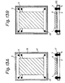
- FIGS. 2A and 2B show Prior Art 6 taught in previously mentioned Japanese Patent Laid-Open Publication No. 2-310957.
- a semiconductor device 40 is produced which has leads 37 on the opposite sides, top and bottom of a package implemented as a molding 38. Then, as shown in FIG. 2B, such semiconductor devices 40 are connected by the leads 37 in multiple stages.
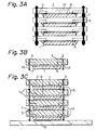
- a semiconductor package stack module has LSI chips 1 implemented as 4M-DRAM chips by way of example. Each chip is sized 4.5 mm x 12.0 mm and provided with twenty-six I/O terminals.
- Ceramic carrier substrates 2 are implemented as 150 ⁇ m thick glass ceramic substrates in the illustrative embodiment. Each carrier substrate 2 is sized 5.0 mm x 13.4 mm and has wiring conductors 3 on its surface where the chip 1 is mounted, and in its inside. For the conductors 3, use is made of an Ag-Pd conductive paste.
- the carrier substrates 2 are formed with through holes 5 in their portions where the substrates 2 are electrically connected to each other. The front and rear of each carrier substrate 2 is connected together by a conductor.
- Each chip 1 and associated carrier substrate 2 are connected by bumps 4 which are implemented by a Pb-Sn solder.
- the reference numeral 12 designates a mother board.
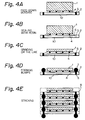
- the above stack module was connected by the following procedure. First, the bumps 4 were formed on each chip 1. Then, a solder paste was printed on the pads of the carrier substrate 2, and then the chip 1 was set on the substrate 2. The substrate 2 and chip 1 were connected together by reflow at 230°C (FIG. 4A). The substrate 2 has a capacitor 10 thereinside. An epoxy resin or seal resin 6 was injected into the above subassembly and then hardened in order to enhance the reliability of the connecting portion and chip 1 (FIG. 4B). The chip 1 was produced from a 0.6 mm thick silicon wafer and ground, polished, surface ground, etched or otherwise treated to a thickness of 0.1 mm (FIG. 4C).
- the bumps 7 are Cu balls having a diameter of 150 ⁇ m and coated with a Pb-Sn solder. Specifically, the solder paste was printed on the pads of each substrate 2, and then the Cu balls coated with solder were arranged on the substrate 2 and fused by heat to turn out the bumps 7 (FIG. 4D). The solder paste was also printed on the other side of each substrate 2. Subsequently, four substrates 2 were stacked and heated to be thereby connected to each other and then fixed by a resin 8. The resulting stack module is shown in FIG. 4E.
- the four 4M-DRAMs stacked together implement a 16M-DRAM. Because the thickness of the module is open to choice, the individual semiconductor device can be as thin as 0.1 mm to 0.3 mm.
- the substrates 2 have desirably flat because the warp thereof is 20 ⁇ m or less.
- an Ag-Pd conductor is plated with Ni and Au in order to enhance the wettability of the solder.
- the substrates 2 are formed of glass ceramics based on lead borosilicate.
- use may be made of lead borosilicate-based steatite, forsterite, cordierite, mullite or similar insulative glass ceramics, or alumina, mullite, aluminum nitride, silicone nitride or similar ceramics.
- the substrates 2 are formed of such strong ceramics, they are substantially free from deformation during assembly. Hence, the stack module is desirable in operability and reliability.
- solder whose major component was Pb-Sn could be replaced with a solder whose major component was Sn-Ag, Sn-Zn, Au or In. Because each material has a particular melting temperature, it is necessary to select an adequate combination of solders, adequate processing temperatures, etc.
- bumps may also be implemented by the material used for the solder, use may be made of Cu-core balls or Ni-, Fe- or similar metal-core balls.
- the bumps may even be replaced with conductive pins 13, as shown in FIGS. 3B and 3C.
- the conductive adhesive may be an epoxy resin containing the particles of Ag, Cu, Au or similar conductive metal.
- each substrate 2 may be elongated in the right-and-left direction, as viewed in FIG. 3A. This allows the substrates 2 to play the role of cooling fins.
- This embodiment is similar to the first embodiment except that carrier films are substituted for the carrier substrates 2.
- the carrier films were implemented by 100 ⁇ m thick polyimide films sized 5.0 mm x 13.4 mm.
- the Cu wiring conductors 3 were formed on the surface of each carrier film where the chip 1 was mounted.
- FIG. 5A shows a single carrier substrate although a plurality of such substrates may be stacked to form a stack module.
- the substrate was made of alumina and 100 ⁇ m thick, while the wiring conductors were implemented by Mo.
- the substrate is formed with a cavity 21 for receiving an LSI chip.
- the bumps for connecting the chip to the substrate was implemented by an Au-Sn solder.
- the substrates stacked together were connected to each other by an Sn-Zn solder.
- this embodiment is similar to the third embodiment except that a carrier film is substituted for the carrier substrate.
- the wiring conductors were implemented by Cu.
- the film was 100 ⁇ m thick in its portion corresponding to the cavity 21, and 250 ⁇ m thick in the other portion.
- the carrier with the cavity 21 of the third or fourth embodiment is easy to handle in the event of stacking and protects the chip from damage. This kind of package is highly reliable.
- the nearby carriers or all the carriers in the stack may be collectively sealed by a nonconductive resin 14, except for the bumps 7 to be connected to the mother board 12. This increases the resistance of the module to moisture.
- the nonconductive resin 14 is also applicable to the carriers lacking the cavity.
- FIGS. 7A-7D show a procedure for assembling the stack of FIG. 6.
- the LSI chip 1 with metal or bumps 4 is connected face down to the carrier 2 having the cavity 21, and the electrodes of the chip 1 and those of the carrier 2 are electrically connected (FIG. 7A).
- the subassembly is sealed by the resin 6 (FIG. 7B).
- the chip 1 has its rear polished, ground, etched or otherwise treated to have a thickness of about 0.1 mm to about 0.3 mm (FIG. 7C).
- the carriers are stacked together and connected by metal, conductive resin or the like via the end through holds 5' (FIG. 7D).
- the entire stack is about 0.4 mm to 1.2 mm thick. While such a thickness is equivalent to 0.1 mm particular to a TSOP which is the thinnest package available today, this embodiment is about four times as high as the TSOP in packaging density and feasible for a high density semiconductor device.
- FIG. 8 shows a single carrier substrate 2 although a plurality of such substrates may be stacked to form a stack module.
- the LSI chip 1 is bonded to the semiconductor pads of the substrate 2 face down via the bumps 4.
- the ceramic substrate 2 was 200 ⁇ m thick. Increases in processing speed and packaging density make it necessary to release heat generated by the chip 1 and to match the characteristic impedance.
- a conductor layer 11 is formed on the side of the substrate 2 opposite to the side for mounting the chip 1.
- the conductor layer 11 may be implemented as a conductive heat radiator, in which case the layer 11 may be connected to ground. While the conductive layer 11 is W in the embodiment, the above object is achievable even if use is made of metal whose major component is Ag, Au, Cu, Ag-Pd, Mo or the like.
- the ceramic carrier 2 is formed of aluminum nitride.
- the carrier 2 may be formed of any other glass ceramics or ceramics mentioned in relation to the first embodiment.
- the wiring conductors 3 were based on W.
- the bumps 4 and 7 were implemented by Ag-core balls coated with an Sn-Ag solder and Au, respectively.
- this embodiment is similar to the sixth embodiment except that the ceramic carrier substrate 2 is replaced with a 50 ⁇ m thick polyimide carrier film 2.
- a heat radiator 9 is formed on the side of the film 2 opposite to the side for mounting the chip 1.
- the heat radiator 9, it is possible to radiate the heat and to match the characteristic impedance for reducing electric noise.
- the heat radiator, or conductive layer, 9 may be formed in a solid, mesh or similar pattern. While the heat radiator 9 is a copper sheet in the embodiment, use may be made of a sheet of nickel, stainless steel, tungsten, aluminum, molybdenum or similar metal. Further, as shown in FIGS. 9B and 9C, the heat radiator 9 may be bonded by metal or resin having high thermal conductivity to the rear of the individual chip I thinned to a desired thickness.
- the bumps 7 and 4 were implemented by Ag-core balls coated with an Sn-Ag solder and Au, respectively.
- a Cu conductor was plated with Ni and Au.
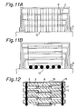
- FIGS. 10a and 10B show an embodiment in which the carriers 2 arranged in a stack each has a heat radiating effect.
- each heat radiator 9 is elongated in order to enhance the heat radiating effect. Because the heat radiating effect of the heat radiator 9 increases with an increase in the thickness of the radiator 9, the distance between the chip 1 and the carrier 2 should preferably be zero. If the distance is not zero, a compound, silicone rubber or oil having high thermal conductivity may be filled in the gap between the chip 1 and the carrier 2.
- FIGS. 10A and 10B show each heat radiator 9 as contacting the rear of the associated chip 1, the heat radiator 9 may, of course, contact the rear of the carrier 2.
- the chips 1 each having the respective heat radiator 9 are mounted on the mother board 12.
- the surface of the heat radiator 9 and the rear of the associated carrier 2 may be bonded by metal or resin having high thermal conductivity, as shown in FIG. 11A, or may be connected together by bumps, as shown in FIG. 11B.
- This kind of structure implements a semiconductor package stack module having a high density and releasing heat efficiently.
- electrodes 15 formed on the uppermost carrier substrate 2 are covered with an insulator 16, e.g., a polyimide type sheet.
- the insulator 16 is provided with an adhesive layer on its one side. In this condition, even when a conductive impurity deposits on any of the electrodes 15, the package is free from short-circuiting. After the stack has been mounted to the mother board, the insulator 16 may be removed in order to use the electrodes 15 as test pads.
- FIG. 13A shows the carrier 2 formed with though holes 17 at a fine pitch, in addition to the through holes 5 adapted for carrier connection.
- the through holes 17 are interconnected by a conductor 18, and all of them are connected to a ground terminal 19.
- FIG. 13B shows the carrier 2 provided with a conductive layer 20 along its edges.
- the conductive layer 20 is connected to the ground terminal 19.
- the conductive layer 20 surrounds the chip 1 and thereby prevents it from interfering with another chip 1.
- a multicarrier body is formed with a number of carriers 2 shown in FIGS. 4A-4E or 7A-7D.
- the chips 1 are connected to the multicarrier body by bumps.
- the seal resin 6 is injected between each chip 1 and the associated carrier 2.
- the rear of each chip 1 is ground, polished, etched or otherwise treated to provide the chip 1 with a desired thickness.
- the bumps 7 having a desired height are formed by a solder ball method, solder paste printing method, dispensing method, or similar technology.
- Terminals extending out from the individual chip 1 to the associated carrier 2 are used to test the electric characteristic before, during, or after a burn-in test. It is to be noted that such a test can be effected at any desired stage after the chips 1 have been mounted on the multicarrier body. A desired number of carriers undergone the above test are positioned. The carriers are connected together by reflow, welding or similar technology when the connection is implemented by metal, or they are connected by thermosetting, ultraviolet rays setting or similar technology when use is made of a conductive resin.
- the individual semiconductor device is produced by dicing, laser, scribing, choco-braking, or similar technology.
- the initial multicarrier body is formed with brake grooves.
- an electric characteristic test is performed, as needed. For the test, electrical contact with pads for stack connection and formed on the top, bottom and opposite sides of the individual carrier is set up by a probe or surface-to-surface contact.
- the present invention provides a semiconductor package stack module and a method of producing it which have various unprecedented advantages, as enumerated below.
Landscapes
- Wire Bonding (AREA)
- Structures Or Materials For Encapsulating Or Coating Semiconductor Devices Or Solid State Devices (AREA)
Applications Claiming Priority (3)
| Application Number | Priority Date | Filing Date | Title |
|---|---|---|---|
| JP3666495 | 1995-02-24 | ||
| JP36664/95 | 1995-02-24 | ||
| JP7036664A JP2944449B2 (ja) | 1995-02-24 | 1995-02-24 | 半導体パッケージとその製造方法 |
Publications (2)
| Publication Number | Publication Date |
|---|---|
| EP0729184A2 true EP0729184A2 (de) | 1996-08-28 |
| EP0729184A3 EP0729184A3 (de) | 1999-11-03 |
Family
ID=12476134
Family Applications (1)
| Application Number | Title | Priority Date | Filing Date |
|---|---|---|---|
| EP96102773A Withdrawn EP0729184A3 (de) | 1995-02-24 | 1996-02-23 | Stapelmodul von Halbleiterpackungen und Herstellungsverfahren |
Country Status (5)
| Country | Link |
|---|---|
| US (1) | US6188127B1 (de) |
| EP (1) | EP0729184A3 (de) |
| JP (1) | JP2944449B2 (de) |
| KR (1) | KR100231366B1 (de) |
| TW (1) | TW312844B (de) |
Cited By (11)
| Publication number | Priority date | Publication date | Assignee | Title |
|---|---|---|---|---|
| WO1999057765A1 (en) * | 1998-05-05 | 1999-11-11 | Dense-Pac Microsystems, Inc. | Chip stack and method of making same |
| EP1028463A1 (de) * | 1999-01-18 | 2000-08-16 | Kabushiki Kaisha Toshiba | Flexibles Gehäuse mit sehr dünnem Halbleiterchip, Modul und Multichip-Modul aus dem Gehäuse zusammengebaut und Herstellungsverfahren |
| US6506664B1 (en) | 1999-04-02 | 2003-01-14 | Imec Vzw | Method of transferring ultra-thin substrates and application of the method to the manufacture of a multi-layer thin film device |
| EP0915516A3 (de) * | 1997-10-30 | 2004-01-02 | Nec Corporation | Substrat für Einbaumodul und Einbaumodul |
| EP1137066A3 (de) * | 2000-03-24 | 2004-12-22 | Shinko Electric Industries Co. Ltd. | Halbleiter und seine Herstellung |
| KR100556177B1 (ko) * | 2000-09-05 | 2006-03-03 | 세이코 엡슨 가부시키가이샤 | 반도체 장치 및 그 제조 방법, 회로 기판 및 전자 기기 |
| CN102945821A (zh) * | 2012-11-28 | 2013-02-27 | 贵州振华风光半导体有限公司 | 高密度厚膜混合集成电路的集成方法 |
| CN103094219A (zh) * | 2012-11-28 | 2013-05-08 | 贵州振华风光半导体有限公司 | 三维集成高密度厚膜多芯片组件的集成方法 |
| EP2693477A4 (de) * | 2011-12-21 | 2014-02-05 | Huawei Tech Co Ltd | Pop-verkapselungsstruktur |
| EP3055881A4 (de) * | 2014-12-15 | 2017-09-13 | INTEL Corporation | Opossum-chip-on-chip-maschenverschlussvorrichtung |
| CN113410193A (zh) * | 2021-05-27 | 2021-09-17 | 力成科技(苏州)有限公司 | 一种8+1堆叠式芯片封装装置 |
Families Citing this family (163)
| Publication number | Priority date | Publication date | Assignee | Title |
|---|---|---|---|---|
| JP2728074B2 (ja) * | 1995-12-28 | 1998-03-18 | 日本電気株式会社 | テープキャリアパッケージのスタック構造 |
| DE19626126C2 (de) * | 1996-06-28 | 1998-04-16 | Fraunhofer Ges Forschung | Verfahren zur Ausbildung einer räumlichen Chipanordnung und räumliche Chipanordung |
| KR100447313B1 (ko) | 1996-11-21 | 2004-09-07 | 가부시키가이샤 히타치세이사쿠쇼 | 반도체 장치 및 그 제조방법 |
| KR100381836B1 (ko) * | 1996-12-13 | 2003-07-18 | 앰코 테크놀로지 코리아 주식회사 | 반도체패키지 |
| JPH10294423A (ja) * | 1997-04-17 | 1998-11-04 | Nec Corp | 半導体装置 |
| JP2000208698A (ja) | 1999-01-18 | 2000-07-28 | Toshiba Corp | 半導体装置 |
| US6274929B1 (en) | 1998-09-01 | 2001-08-14 | Texas Instruments Incorporated | Stacked double sided integrated circuit package |
| US6451624B1 (en) * | 1998-06-05 | 2002-09-17 | Micron Technology, Inc. | Stackable semiconductor package having conductive layer and insulating layers and method of fabrication |
| US6297548B1 (en) | 1998-06-30 | 2001-10-02 | Micron Technology, Inc. | Stackable ceramic FBGA for high thermal applications |
| KR100424188B1 (ko) * | 1998-09-21 | 2004-05-17 | 주식회사 하이닉스반도체 | 칩 사이즈 스택 패키지 |
| US6600364B1 (en) | 1999-01-05 | 2003-07-29 | Intel Corporation | Active interposer technology for high performance CMOS packaging application |
| US6461895B1 (en) * | 1999-01-05 | 2002-10-08 | Intel Corporation | Process for making active interposer for high performance packaging applications |
| JP2000216334A (ja) | 1999-01-25 | 2000-08-04 | Seiko Epson Corp | 半導体装置 |
| JP3627565B2 (ja) * | 1999-03-30 | 2005-03-09 | セイコーエプソン株式会社 | 半導体装置およびその製造方法 |
| JP2000315866A (ja) * | 1999-04-30 | 2000-11-14 | Ibiden Co Ltd | 多層配線板およびその製造方法 |
| JP2000340737A (ja) * | 1999-05-31 | 2000-12-08 | Mitsubishi Electric Corp | 半導体パッケージとその実装体 |
| KR100333384B1 (ko) | 1999-06-28 | 2002-04-18 | 박종섭 | 칩 사이즈 스택 패키지 및 그의 제조방법 |
| KR100333385B1 (ko) | 1999-06-29 | 2002-04-18 | 박종섭 | 웨이퍼 레벨 스택 패키지 및 그의 제조 방법 |
| WO2001008222A1 (fr) | 1999-07-22 | 2001-02-01 | Seiko Epson Corporation | Dispositif a semi-conducteur, son procede de fabrication, carte de circuit imprime et dispositif electronique |
| TW417839U (en) * | 1999-07-30 | 2001-01-01 | Shen Ming Tung | Stacked memory module structure and multi-layered stacked memory module structure using the same |
| TW472330B (en) | 1999-08-26 | 2002-01-11 | Toshiba Corp | Semiconductor device and the manufacturing method thereof |
| KR100338929B1 (ko) * | 1999-09-27 | 2002-05-30 | 박종섭 | 적층형 마이크로 비지에이 패키지 및 제조방법 |
| JP2001127088A (ja) * | 1999-10-27 | 2001-05-11 | Mitsubishi Electric Corp | 半導体装置 |
| JP2001144218A (ja) * | 1999-11-17 | 2001-05-25 | Sony Corp | 半導体装置及び半導体装置の製造方法 |
| JP3798597B2 (ja) | 1999-11-30 | 2006-07-19 | 富士通株式会社 | 半導体装置 |
| KR100584003B1 (ko) * | 1999-12-02 | 2006-05-29 | 삼성전자주식회사 | 적층 칩 패키지의 제조 방법 |
| JP4320492B2 (ja) * | 1999-12-08 | 2009-08-26 | 株式会社デンソー | 半導体素子の実装構造および半導体素子の実装構造の製造方法 |
| JP4251421B2 (ja) * | 2000-01-13 | 2009-04-08 | 新光電気工業株式会社 | 半導体装置の製造方法 |
| US6528870B2 (en) * | 2000-01-28 | 2003-03-04 | Kabushiki Kaisha Toshiba | Semiconductor device having a plurality of stacked wiring boards |
| US6780672B2 (en) * | 2000-01-31 | 2004-08-24 | Lockheed Martin Corporation | Micro eletro-mechanical component and system architecture |
| JP3752949B2 (ja) * | 2000-02-28 | 2006-03-08 | 日立化成工業株式会社 | 配線基板及び半導体装置 |
| JP2001250907A (ja) * | 2000-03-08 | 2001-09-14 | Toshiba Corp | 半導体装置及びその製造方法 |
| JP2001267492A (ja) * | 2000-03-14 | 2001-09-28 | Ibiden Co Ltd | 半導体モジュールの製造方法 |
| KR100464561B1 (ko) * | 2000-04-11 | 2004-12-31 | 앰코 테크놀로지 코리아 주식회사 | 반도체 패키지 및 이것의 제조방법 |
| KR100631934B1 (ko) * | 2000-06-28 | 2006-10-04 | 주식회사 하이닉스반도체 | 스택 패키지 |
| JP3951091B2 (ja) * | 2000-08-04 | 2007-08-01 | セイコーエプソン株式会社 | 半導体装置の製造方法 |
| JP3874062B2 (ja) | 2000-09-05 | 2007-01-31 | セイコーエプソン株式会社 | 半導体装置 |
| TW503531B (en) * | 2000-09-28 | 2002-09-21 | Toshiba Corp | Multi-layered semiconductor apparatus |
| JP2002176137A (ja) | 2000-09-28 | 2002-06-21 | Toshiba Corp | 積層型半導体デバイス |
| US7414319B2 (en) * | 2000-10-13 | 2008-08-19 | Bridge Semiconductor Corporation | Semiconductor chip assembly with metal containment wall and solder terminal |
| US7129575B1 (en) | 2000-10-13 | 2006-10-31 | Bridge Semiconductor Corporation | Semiconductor chip assembly with bumped metal pillar |
| US6876072B1 (en) | 2000-10-13 | 2005-04-05 | Bridge Semiconductor Corporation | Semiconductor chip assembly with chip in substrate cavity |
| US7319265B1 (en) | 2000-10-13 | 2008-01-15 | Bridge Semiconductor Corporation | Semiconductor chip assembly with precision-formed metal pillar |
| US7190080B1 (en) | 2000-10-13 | 2007-03-13 | Bridge Semiconductor Corporation | Semiconductor chip assembly with embedded metal pillar |
| US7009297B1 (en) | 2000-10-13 | 2006-03-07 | Bridge Semiconductor Corporation | Semiconductor chip assembly with embedded metal particle |
| US7075186B1 (en) | 2000-10-13 | 2006-07-11 | Bridge Semiconductor Corporation | Semiconductor chip assembly with interlocked contact terminal |
| US7071089B1 (en) | 2000-10-13 | 2006-07-04 | Bridge Semiconductor Corporation | Method of making a semiconductor chip assembly with a carved bumped terminal |
| US7129113B1 (en) | 2000-10-13 | 2006-10-31 | Bridge Semiconductor Corporation | Method of making a three-dimensional stacked semiconductor package with a metal pillar in an encapsulant aperture |
| US6872591B1 (en) | 2000-10-13 | 2005-03-29 | Bridge Semiconductor Corporation | Method of making a semiconductor chip assembly with a conductive trace and a substrate |
| US7094676B1 (en) | 2000-10-13 | 2006-08-22 | Bridge Semiconductor Corporation | Semiconductor chip assembly with embedded metal pillar |
| US7262082B1 (en) | 2000-10-13 | 2007-08-28 | Bridge Semiconductor Corporation | Method of making a three-dimensional stacked semiconductor package with a metal pillar and a conductive interconnect in an encapsulant aperture |
| US7132741B1 (en) | 2000-10-13 | 2006-11-07 | Bridge Semiconductor Corporation | Semiconductor chip assembly with carved bumped terminal |
| JP2002134650A (ja) * | 2000-10-23 | 2002-05-10 | Rohm Co Ltd | 半導体装置およびその製造方法 |
| JP3420748B2 (ja) * | 2000-12-14 | 2003-06-30 | 松下電器産業株式会社 | 半導体装置及びその製造方法 |
| KR20020049145A (ko) * | 2000-12-19 | 2002-06-26 | 박종섭 | 반도체 패키지 제조용 절연 테이프와 그를 이용한 반도체패키지 |
| JP2002305286A (ja) * | 2001-02-01 | 2002-10-18 | Mitsubishi Electric Corp | 半導体モジュールおよび電子部品 |
| TW575949B (en) * | 2001-02-06 | 2004-02-11 | Hitachi Ltd | Mixed integrated circuit device, its manufacturing method and electronic apparatus |
| DE10110203B4 (de) * | 2001-03-02 | 2006-12-14 | Infineon Technologies Ag | Elektronisches Bauteil mit gestapelten Halbleiterchips und Verfahren zu seiner Herstellung |
| JP2002270634A (ja) * | 2001-03-08 | 2002-09-20 | Rohm Co Ltd | 半導体装置 |
| EP1389897A1 (de) * | 2001-04-24 | 2004-02-18 | Mitsui Mining & Smelting Co., Ltd. | Leiterplatte, verfahren zu ihrer herstellung und csp-herstellungsverfahren |
| US20020173077A1 (en) * | 2001-05-03 | 2002-11-21 | Ho Tzong Da | Thermally enhanced wafer-level chip scale package and method of fabricating the same |
| JP3631445B2 (ja) * | 2001-06-06 | 2005-03-23 | 東芝三菱電機産業システム株式会社 | 平型半導体スタック装置 |
| JP3660275B2 (ja) * | 2001-06-14 | 2005-06-15 | シャープ株式会社 | 半導体装置およびその製造方法 |
| US20020190367A1 (en) * | 2001-06-15 | 2002-12-19 | Mantz Frank E. | Slice interconnect structure |
| KR100437539B1 (ko) * | 2001-06-29 | 2004-06-26 | 주식회사 하이닉스반도체 | 클럭 동기 회로 |
| JP3925615B2 (ja) * | 2001-07-04 | 2007-06-06 | ソニー株式会社 | 半導体モジュール |
| US6765287B1 (en) | 2001-07-27 | 2004-07-20 | Charles W. C. Lin | Three-dimensional stacked semiconductor package |
| US6451626B1 (en) | 2001-07-27 | 2002-09-17 | Charles W.C. Lin | Three-dimensional stacked semiconductor package |
| JP4023159B2 (ja) * | 2001-07-31 | 2007-12-19 | ソニー株式会社 | 半導体装置の製造方法及び積層半導体装置の製造方法 |
| US6790710B2 (en) | 2002-01-31 | 2004-09-14 | Asat Limited | Method of manufacturing an integrated circuit package |
| JP2003078108A (ja) * | 2001-08-31 | 2003-03-14 | Hitachi Chem Co Ltd | 半導体パッケージ用基板、これを用いた半導体パッケージとその積層体、およびこれらの製造方法 |
| US6573460B2 (en) * | 2001-09-20 | 2003-06-03 | Dpac Technologies Corp | Post in ring interconnect using for 3-D stacking |
| US6573461B2 (en) | 2001-09-20 | 2003-06-03 | Dpac Technologies Corp | Retaining ring interconnect used for 3-D stacking |
| US7253091B2 (en) * | 2001-09-28 | 2007-08-07 | Hrl Laboratories, Llc | Process for assembling three-dimensional systems on a chip and structure thus obtained |
| JP3861669B2 (ja) * | 2001-11-22 | 2006-12-20 | ソニー株式会社 | マルチチップ回路モジュールの製造方法 |
| KR100486832B1 (ko) * | 2002-02-06 | 2005-05-03 | 삼성전자주식회사 | 반도체 칩과 적층 칩 패키지 및 그 제조 방법 |
| US6750082B2 (en) * | 2002-09-13 | 2004-06-15 | Advanpack Solutions Pte. Ltd. | Method of assembling a package with an exposed die backside with and without a heatsink for flip-chip |
| US6856010B2 (en) * | 2002-12-05 | 2005-02-15 | Staktek Group L.P. | Thin scale outline package |
| KR100484088B1 (ko) * | 2002-12-06 | 2005-04-20 | 삼성전자주식회사 | 멀티 칩 패키지용 다이 어태치와 경화 인라인 장치 |
| US20040207990A1 (en) * | 2003-04-21 | 2004-10-21 | Rose Andrew C. | Stair-step signal routing |
| JP2004335624A (ja) * | 2003-05-06 | 2004-11-25 | Hitachi Ltd | 半導体モジュール |
| TWI231023B (en) * | 2003-05-27 | 2005-04-11 | Ind Tech Res Inst | Electronic packaging with three-dimensional stack and assembling method thereof |
| JP3858854B2 (ja) * | 2003-06-24 | 2006-12-20 | 富士通株式会社 | 積層型半導体装置 |
| US20040262728A1 (en) * | 2003-06-30 | 2004-12-30 | Sterrett Terry L. | Modular device assemblies |
| KR100506035B1 (ko) * | 2003-08-22 | 2005-08-03 | 삼성전자주식회사 | 반도체 패키지 및 그 제조방법 |
| US7180165B2 (en) * | 2003-09-05 | 2007-02-20 | Sanmina, Sci Corporation | Stackable electronic assembly |
| US7993983B1 (en) | 2003-11-17 | 2011-08-09 | Bridge Semiconductor Corporation | Method of making a semiconductor chip assembly with chip and encapsulant grinding |
| KR100621992B1 (ko) * | 2003-11-19 | 2006-09-13 | 삼성전자주식회사 | 이종 소자들의 웨이퍼 레벨 적층 구조와 방법 및 이를이용한 시스템-인-패키지 |
| US7425759B1 (en) | 2003-11-20 | 2008-09-16 | Bridge Semiconductor Corporation | Semiconductor chip assembly with bumped terminal and filler |
| US7538415B1 (en) | 2003-11-20 | 2009-05-26 | Bridge Semiconductor Corporation | Semiconductor chip assembly with bumped terminal, filler and insulative base |
| JP3821125B2 (ja) * | 2003-12-18 | 2006-09-13 | セイコーエプソン株式会社 | 半導体装置の製造方法、半導体装置、回路基板、電子機器 |
| US7227249B1 (en) | 2003-12-24 | 2007-06-05 | Bridge Semiconductor Corporation | Three-dimensional stacked semiconductor package with chips on opposite sides of lead |
| US7126829B1 (en) * | 2004-02-09 | 2006-10-24 | Pericom Semiconductor Corp. | Adapter board for stacking Ball-Grid-Array (BGA) chips |
| JP4280179B2 (ja) * | 2004-02-27 | 2009-06-17 | 新光電気工業株式会社 | 積層型半導体装置 |
| JP4205613B2 (ja) | 2004-03-01 | 2009-01-07 | エルピーダメモリ株式会社 | 半導体装置 |
| DE112004002858T5 (de) | 2004-05-11 | 2007-04-19 | Spansion Llc, Sunnyvale | Träger für eine Stapel-Halbleitervorrichtung und Verfahren zum Herstellen derselben |
| GB2429842B (en) | 2004-05-20 | 2009-01-28 | Spansion Llc | Method of fabricating semiconductor device and semiconductor device |
| JP4561969B2 (ja) * | 2004-05-26 | 2010-10-13 | セイコーエプソン株式会社 | 半導体装置 |
| US6987314B1 (en) * | 2004-06-08 | 2006-01-17 | Amkor Technology, Inc. | Stackable semiconductor package with solder on pads on which second semiconductor package is stacked |
| US7282791B2 (en) * | 2004-07-09 | 2007-10-16 | Elpida Memory, Inc. | Stacked semiconductor device and semiconductor memory module |
| KR20060018453A (ko) * | 2004-08-24 | 2006-03-02 | 삼성전자주식회사 | 히트 싱크를 갖는 반도체 소자 |
| US20060048385A1 (en) * | 2004-09-03 | 2006-03-09 | Staktek Group L.P. | Minimized profile circuit module systems and methods |
| US7498666B2 (en) * | 2004-09-27 | 2009-03-03 | Nokia Corporation | Stacked integrated circuit |
| WO2006035528A1 (ja) | 2004-09-29 | 2006-04-06 | Murata Manufacturing Co., Ltd. | スタックモジュール及びその製造方法 |
| JP4014591B2 (ja) * | 2004-10-05 | 2007-11-28 | シャープ株式会社 | 半導体装置および電子機器 |
| WO2006043388A1 (ja) * | 2004-10-21 | 2006-04-27 | Matsushita Electric Industrial Co., Ltd. | 半導体内蔵モジュール及びその製造方法 |
| US7446419B1 (en) | 2004-11-10 | 2008-11-04 | Bridge Semiconductor Corporation | Semiconductor chip assembly with welded metal pillar of stacked metal balls |
| US7750483B1 (en) | 2004-11-10 | 2010-07-06 | Bridge Semiconductor Corporation | Semiconductor chip assembly with welded metal pillar and enlarged plated contact terminal |
| US7268421B1 (en) | 2004-11-10 | 2007-09-11 | Bridge Semiconductor Corporation | Semiconductor chip assembly with welded metal pillar that includes enlarged ball bond |
| KR100639702B1 (ko) * | 2004-11-26 | 2006-10-30 | 삼성전자주식회사 | 패키지된 반도체 다이 및 그 제조방법 |
| US7183638B2 (en) * | 2004-12-30 | 2007-02-27 | Intel Corporation | Embedded heat spreader |
| JP2006196709A (ja) * | 2005-01-13 | 2006-07-27 | Sharp Corp | 半導体装置およびその製造方法 |
| WO2006088270A1 (en) * | 2005-02-15 | 2006-08-24 | Unisemicon Co., Ltd. | Stacked package and method of fabricating the same |
| JP5116268B2 (ja) * | 2005-08-31 | 2013-01-09 | キヤノン株式会社 | 積層型半導体装置およびその製造方法 |
| CN100481420C (zh) * | 2005-09-08 | 2009-04-22 | 南茂科技股份有限公司 | 堆叠型芯片封装结构、芯片封装体及其制造方法 |
| US8389867B2 (en) * | 2005-09-30 | 2013-03-05 | Ibiden Co., Ltd. | Multilayered circuit substrate with semiconductor device incorporated therein |
| JP2007123753A (ja) * | 2005-10-31 | 2007-05-17 | National Institute Of Advanced Industrial & Technology | インターポーザ、半導体チップユニットおよび半導体チップ積層モジュール、ならびに製造方法 |
| EP2290682A3 (de) | 2005-12-14 | 2011-10-05 | Shinko Electric Industries Co., Ltd. | Gehäuse mit einem zwischen zwei Substraten eingebetteten Chip und Herstellungsverfahren dafür |
| US8067267B2 (en) * | 2005-12-23 | 2011-11-29 | Tessera, Inc. | Microelectronic assemblies having very fine pitch stacking |
| US7990727B1 (en) * | 2006-04-03 | 2011-08-02 | Aprolase Development Co., Llc | Ball grid array stack |
| US7494843B1 (en) | 2006-12-26 | 2009-02-24 | Bridge Semiconductor Corporation | Method of making a semiconductor chip assembly with thermal conductor and encapsulant grinding |
| US7811863B1 (en) | 2006-10-26 | 2010-10-12 | Bridge Semiconductor Corporation | Method of making a semiconductor chip assembly with metal pillar and encapsulant grinding and heat sink attachment |
| TWI312561B (en) * | 2006-10-27 | 2009-07-21 | Advanced Semiconductor Eng | Structure of package on package and method for fabricating the same |
| JP4917874B2 (ja) * | 2006-12-13 | 2012-04-18 | 新光電気工業株式会社 | 積層型パッケージ及びその製造方法 |
| JP4591715B2 (ja) * | 2007-03-30 | 2010-12-01 | セイコーエプソン株式会社 | 半導体装置の製造方法 |
| JP2008311267A (ja) * | 2007-06-12 | 2008-12-25 | Taiyo Yuden Co Ltd | 回路モジュールの製造方法及び回路モジュール |
| JP5054440B2 (ja) * | 2007-06-15 | 2012-10-24 | 新光電気工業株式会社 | 電子部品内蔵基板の製造方法及び電子部品内蔵基板 |
| JP2009094152A (ja) | 2007-10-04 | 2009-04-30 | Hitachi Ltd | 半導体装置、その製造方法及び半導体搭載用フレキシブル基板 |
| US8074581B2 (en) | 2007-10-12 | 2011-12-13 | Steelcase Inc. | Conference table assembly |
| US9024455B2 (en) * | 2010-05-26 | 2015-05-05 | Hitachi Chemical Company, Ltd. | Semiconductor encapsulation adhesive composition, semiconductor encapsulation film-like adhesive, method for producing semiconductor device and semiconductor device |
| JP4550102B2 (ja) * | 2007-10-25 | 2010-09-22 | スパンション エルエルシー | 半導体パッケージ及びその製造方法、半導体パッケージを備える半導体装置 |
| TWI355061B (en) * | 2007-12-06 | 2011-12-21 | Nanya Technology Corp | Stacked-type chip package structure and fabricatio |
| JP5153364B2 (ja) * | 2008-01-30 | 2013-02-27 | 京セラ株式会社 | 積層型半導体パッケージおよび電子装置 |
| KR100936070B1 (ko) * | 2008-02-26 | 2010-01-12 | 재단법인 서울테크노파크 | 웨이퍼 스택 제작 방법 |
| JP5174518B2 (ja) * | 2008-04-17 | 2013-04-03 | スパンション エルエルシー | 積層型半導体装置、及びその製造方法 |
| SG142321A1 (en) * | 2008-04-24 | 2009-11-26 | Micron Technology Inc | Pre-encapsulated cavity interposer |
| KR100997793B1 (ko) | 2008-09-01 | 2010-12-02 | 주식회사 하이닉스반도체 | 반도체 패키지 및 이의 제조 방법 |
| US10026720B2 (en) * | 2015-05-20 | 2018-07-17 | Broadpak Corporation | Semiconductor structure and a method of making thereof |
| KR20100033012A (ko) * | 2008-09-19 | 2010-03-29 | 주식회사 하이닉스반도체 | 반도체 패키지 및 이를 갖는 적층 반도체 패키지 |
| JP5468242B2 (ja) * | 2008-11-21 | 2014-04-09 | 株式会社東芝 | Memsパッケージおよびmemsパッケージの製造方法 |
| JP4833307B2 (ja) * | 2009-02-24 | 2011-12-07 | インターナショナル・ビジネス・マシーンズ・コーポレーション | 半導体モジュール、端子板、端子板の製造方法および半導体モジュールの製造方法 |
| KR101078733B1 (ko) | 2009-06-29 | 2011-11-02 | 주식회사 하이닉스반도체 | 반도체 패키지 |
| US8310835B2 (en) * | 2009-07-14 | 2012-11-13 | Apple Inc. | Systems and methods for providing vias through a modular component |
| TWI397155B (zh) * | 2009-12-24 | 2013-05-21 | 力成科技股份有限公司 | 形成矽穿孔之多晶片堆疊過程 |
| US8884422B2 (en) * | 2009-12-31 | 2014-11-11 | Stmicroelectronics Pte Ltd. | Flip-chip fan-out wafer level package for package-on-package applications, and method of manufacture |
| JP2012033875A (ja) | 2010-06-30 | 2012-02-16 | Canon Inc | 積層型半導体装置 |
| US8847376B2 (en) | 2010-07-23 | 2014-09-30 | Tessera, Inc. | Microelectronic elements with post-assembly planarization |
| FR2964786B1 (fr) * | 2010-09-09 | 2013-03-15 | Commissariat Energie Atomique | Procédé de réalisation d'éléments a puce munis de rainures d'insertion de fils |
| US20120074558A1 (en) * | 2010-09-29 | 2012-03-29 | Mao Bang Electronic Co., Ltd. | Circuit Board Packaged with Die through Surface Mount Technology |
| US9013037B2 (en) | 2011-09-14 | 2015-04-21 | Stmicroelectronics Pte Ltd. | Semiconductor package with improved pillar bump process and structure |
| US8916481B2 (en) | 2011-11-02 | 2014-12-23 | Stmicroelectronics Pte Ltd. | Embedded wafer level package for 3D and package-on-package applications, and method of manufacture |
| US8513795B2 (en) * | 2011-12-27 | 2013-08-20 | Taiwan Semiconductor Manufacturing Co., Ltd. | 3D IC configuration with contactless communication |
| WO2013118415A1 (ja) * | 2012-02-09 | 2013-08-15 | 富士電機株式会社 | 半導体装置 |
| CN102623359A (zh) * | 2012-04-17 | 2012-08-01 | 日月光半导体制造股份有限公司 | 半导体封装结构及其制造方法 |
| US9548283B2 (en) * | 2012-07-05 | 2017-01-17 | Taiwan Semiconductor Manufacturing Company, Ltd. | Package redistribution layer structure and method of forming same |
| US9685423B2 (en) * | 2013-01-31 | 2017-06-20 | PAC Tech—Packaging Technologies GmbH | Semiconductor chip assembly and method for manufacturing the same |
| JP5763116B2 (ja) * | 2013-03-25 | 2015-08-12 | 株式会社東芝 | 半導体装置の製造方法 |
| JP6216157B2 (ja) | 2013-05-27 | 2017-10-18 | 新光電気工業株式会社 | 電子部品装置及びその製造方法 |
| US9735078B2 (en) * | 2014-04-16 | 2017-08-15 | Infineon Technologies Ag | Device including multiple semiconductor chips and multiple carriers |
| CN108878398B (zh) | 2017-05-16 | 2020-07-21 | 晟碟半导体(上海)有限公司 | 包括导电凸块互连的半导体器件 |
| JP6984183B2 (ja) * | 2017-06-05 | 2021-12-17 | 富士電機株式会社 | 半導体パッケージ、半導体装置および半導体装置の製造方法 |
| TWI848353B (zh) * | 2021-09-02 | 2024-07-11 | 美商愛玻索立克公司 | 基板載體以及包括其之基板組合 |
| JP2023183319A (ja) * | 2022-06-15 | 2023-12-27 | 新光電気工業株式会社 | 積層基板及び積層基板の製造方法 |
Family Cites Families (37)
| Publication number | Priority date | Publication date | Assignee | Title |
|---|---|---|---|---|
| JPS574127A (en) | 1980-06-10 | 1982-01-09 | Fujitsu Ltd | Formation of conductor pattern |
| US5237204A (en) * | 1984-05-25 | 1993-08-17 | Compagnie D'informatique Militaire Spatiale Et Aeronautique | Electric potential distribution device and an electronic component case incorporating such a device |
| JPS61101067A (ja) | 1984-10-24 | 1986-05-19 | Nec Corp | メモリモジユ−ル |
| WO1993013557A1 (fr) * | 1985-02-14 | 1993-07-08 | Yoshiyuki Sato | Structure de montage tridimensionnel de puces a semi-conducteurs |
| US4953005A (en) * | 1987-04-17 | 1990-08-28 | Xoc Devices, Inc. | Packaging system for stacking integrated circuits |
| JP2667689B2 (ja) | 1988-12-29 | 1997-10-27 | 株式会社徳力本店 | 低融点Agはんだ |
| JP2799408B2 (ja) | 1989-12-22 | 1998-09-17 | 株式会社日立製作所 | 半導体装置及びそれを実装した電子装置 |
| JPH02310957A (ja) | 1989-05-26 | 1990-12-26 | Hitachi Ltd | 半導体装置 |
| JPH03295265A (ja) | 1990-04-13 | 1991-12-26 | Hitachi Ltd | マルチチツプ半導体装置 |
| US5043794A (en) * | 1990-09-24 | 1991-08-27 | At&T Bell Laboratories | Integrated circuit package and compact assemblies thereof |
| JP2876773B2 (ja) * | 1990-10-22 | 1999-03-31 | セイコーエプソン株式会社 | プログラム命令語長可変型計算装置及びデータ処理装置 |
| US5216278A (en) * | 1990-12-04 | 1993-06-01 | Motorola, Inc. | Semiconductor device having a pad array carrier package |
| JPH04280695A (ja) * | 1991-03-08 | 1992-10-06 | Hitachi Ltd | 高集積半導体装置及びそれを用いた半導体モジュール |
| JPH04290258A (ja) * | 1991-03-19 | 1992-10-14 | Nec Corp | マルチチップモジュール |
| JPH0574985A (ja) | 1991-04-16 | 1993-03-26 | Nec Corp | 半導体素子の実装構造 |
| JPH0529534A (ja) * | 1991-07-25 | 1993-02-05 | Nec Corp | メモリモジユール |
| JPH05329681A (ja) | 1991-12-10 | 1993-12-14 | Nec Corp | 多層ろう材とその製造方法および接続方法 |
| US5241454A (en) * | 1992-01-22 | 1993-08-31 | International Business Machines Corporation | Mutlilayered flexible circuit package |
| JPH05198708A (ja) | 1992-01-23 | 1993-08-06 | Hitachi Ltd | 半導体集積回路装置 |
| US5222014A (en) | 1992-03-02 | 1993-06-22 | Motorola, Inc. | Three-dimensional multi-chip pad array carrier |
| JP3201637B2 (ja) | 1992-03-06 | 2001-08-27 | 田中電子工業株式会社 | 半導体素子用のはんだバンプ形成材料 |
| JPH05291480A (ja) | 1992-04-07 | 1993-11-05 | Hitachi Ltd | 積層形マルチチップ半導体装置 |
| US5247423A (en) * | 1992-05-26 | 1993-09-21 | Motorola, Inc. | Stacking three dimensional leadless multi-chip module and method for making the same |
| US5343366A (en) * | 1992-06-24 | 1994-08-30 | International Business Machines Corporation | Packages for stacked integrated circuit chip cubes |
| JP2763478B2 (ja) | 1993-07-12 | 1998-06-11 | 京セラ株式会社 | コンデンサ材料及び多層アルミナ質配線基板並びに半導体素子収納用パッケージ |
| JPH06118129A (ja) | 1992-10-08 | 1994-04-28 | Mitsubishi Electric Corp | 半導体装置の評価装置 |
| JPH06232608A (ja) | 1992-10-29 | 1994-08-19 | Nec Corp | 複合マイクロ波回路モジュール |
| JP2812107B2 (ja) | 1992-10-30 | 1998-10-22 | 日本電気株式会社 | 半導体装置 |
| KR100238197B1 (ko) | 1992-12-15 | 2000-01-15 | 윤종용 | 반도체장치 |
| JPH06244056A (ja) | 1992-12-29 | 1994-09-02 | Sumitomo Kinzoku Ceramics:Kk | 半導体素子収納用パッケージ |
| JPH06260566A (ja) * | 1993-03-04 | 1994-09-16 | Sony Corp | ランドグリッドアレイパッケージ及びその作製方法、並びに半導体パッケージ |
| JPH06268101A (ja) * | 1993-03-17 | 1994-09-22 | Hitachi Ltd | 半導体装置及びその製造方法、電子装置、リ−ドフレ−ム並びに実装基板 |
| JPH06275774A (ja) | 1993-03-19 | 1994-09-30 | Fujitsu Ltd | 回路ユニットの接続装置および該接続装置を用いた回路モジュール |
| JPH06302760A (ja) | 1993-04-13 | 1994-10-28 | Matsushita Electric Ind Co Ltd | 半導体装置 |
| JPH06333983A (ja) | 1993-05-19 | 1994-12-02 | Matsushita Electric Ind Co Ltd | 半導体装置およびその製造方法 |
| KR970000214B1 (ko) * | 1993-11-18 | 1997-01-06 | 삼성전자 주식회사 | 반도체 장치 및 그 제조방법 |
| EP0658937A1 (de) * | 1993-12-08 | 1995-06-21 | Hughes Aircraft Company | Aus dielektrischen Bändern hergestellter vertikaler Stapel integrierter Schaltungen aus diskreten Trägern |
-
1995
- 1995-02-24 JP JP7036664A patent/JP2944449B2/ja not_active Expired - Lifetime
-
1996
- 1996-02-20 US US08/604,115 patent/US6188127B1/en not_active Expired - Lifetime
- 1996-02-23 EP EP96102773A patent/EP0729184A3/de not_active Withdrawn
- 1996-02-24 TW TW085102110A patent/TW312844B/zh not_active IP Right Cessation
- 1996-02-24 KR KR1019960004523A patent/KR100231366B1/ko not_active Expired - Fee Related
Cited By (15)
| Publication number | Priority date | Publication date | Assignee | Title |
|---|---|---|---|---|
| EP0915516A3 (de) * | 1997-10-30 | 2004-01-02 | Nec Corporation | Substrat für Einbaumodul und Einbaumodul |
| WO1999057765A1 (en) * | 1998-05-05 | 1999-11-11 | Dense-Pac Microsystems, Inc. | Chip stack and method of making same |
| EP1028463A1 (de) * | 1999-01-18 | 2000-08-16 | Kabushiki Kaisha Toshiba | Flexibles Gehäuse mit sehr dünnem Halbleiterchip, Modul und Multichip-Modul aus dem Gehäuse zusammengebaut und Herstellungsverfahren |
| US6392143B1 (en) | 1999-01-18 | 2002-05-21 | Kabushiki Kaisha Toshiba | Flexible package having very thin semiconductor chip, module and multi chip module (MCM) assembled by the package, and method for manufacturing the same |
| US6506664B1 (en) | 1999-04-02 | 2003-01-14 | Imec Vzw | Method of transferring ultra-thin substrates and application of the method to the manufacture of a multi-layer thin film device |
| US6730997B2 (en) | 1999-04-02 | 2004-05-04 | Imec Vzw | Method of transferring ultra-thin substrates and application of the method to the manufacture of a multi-layered thin film device |
| EP1137066A3 (de) * | 2000-03-24 | 2004-12-22 | Shinko Electric Industries Co. Ltd. | Halbleiter und seine Herstellung |
| KR100556177B1 (ko) * | 2000-09-05 | 2006-03-03 | 세이코 엡슨 가부시키가이샤 | 반도체 장치 및 그 제조 방법, 회로 기판 및 전자 기기 |
| EP2693477A4 (de) * | 2011-12-21 | 2014-02-05 | Huawei Tech Co Ltd | Pop-verkapselungsstruktur |
| US9318407B2 (en) | 2011-12-21 | 2016-04-19 | Huawei Technologies Co., Ltd. | Pop package structure |
| CN102945821A (zh) * | 2012-11-28 | 2013-02-27 | 贵州振华风光半导体有限公司 | 高密度厚膜混合集成电路的集成方法 |
| CN103094219A (zh) * | 2012-11-28 | 2013-05-08 | 贵州振华风光半导体有限公司 | 三维集成高密度厚膜多芯片组件的集成方法 |
| EP3055881A4 (de) * | 2014-12-15 | 2017-09-13 | INTEL Corporation | Opossum-chip-on-chip-maschenverschlussvorrichtung |
| CN113410193A (zh) * | 2021-05-27 | 2021-09-17 | 力成科技(苏州)有限公司 | 一种8+1堆叠式芯片封装装置 |
| CN113410193B (zh) * | 2021-05-27 | 2024-05-03 | 元成科技(苏州)有限公司 | 一种8+1堆叠式芯片封装装置 |
Also Published As
| Publication number | Publication date |
|---|---|
| EP0729184A3 (de) | 1999-11-03 |
| JPH08236694A (ja) | 1996-09-13 |
| TW312844B (de) | 1997-08-11 |
| KR100231366B1 (ko) | 1999-11-15 |
| JP2944449B2 (ja) | 1999-09-06 |
| US6188127B1 (en) | 2001-02-13 |
Similar Documents
| Publication | Publication Date | Title |
|---|---|---|
| US6188127B1 (en) | Semiconductor packing stack module and method of producing the same | |
| US5942795A (en) | Leaded substrate carrier for integrated circuit device and leaded substrate carrier device assembly | |
| US6344683B1 (en) | Stacked semiconductor package with flexible tape | |
| CA1304170C (en) | Highly integrated circuit and method for the production thereof | |
| US5519936A (en) | Method of making an electronic package with a thermally conductive support member having a thin circuitized substrate and semiconductor device bonded thereto | |
| KR0169820B1 (ko) | 금속 회로 기판을 갖는 칩 스케일 패키지 | |
| EP0117111B1 (de) | Halbleiteranordnungszusammenbau | |
| JP2570637B2 (ja) | Mcmキャリア | |
| US5367124A (en) | Compliant lead for surface mounting a chip package to a substrate | |
| JP2949490B2 (ja) | 半導体パッケージの製造方法 | |
| US5633533A (en) | Electronic package with thermally conductive support member having a thin circuitized substrate and semiconductor device bonded thereto | |
| EP0862217A2 (de) | Halbleiteranordnung und Halbleiter-Mehrchipmodul | |
| US20020050407A1 (en) | Ground via structures in semiconductor packages | |
| JPH0785500B2 (ja) | カプセル封じされた半導体パツケージ | |
| TW200828523A (en) | Multi-component package with both top and bottom side connection pads for three-dimensional packaging | |
| US6242283B1 (en) | Wafer level packaging process of semiconductor | |
| KR100226335B1 (ko) | 플라스틱 성형회로 패키지 | |
| EP0704898A2 (de) | Trägerfilm | |
| JPH08279591A (ja) | 半導体装置とその製造方法 | |
| GB2199988A (en) | Multi-layer molded plastic ic package | |
| US6320136B1 (en) | Layered printed-circuit-board and module using the same | |
| EP0408272A2 (de) | Kontaktieren elektrischer Leiter | |
| EP0081419A2 (de) | Hermetische integrierte Schaltungsträger mit hoher Leiterzahl massenweise verbunden | |
| EP0170022B1 (de) | Packung einer Leistungshalbleiteranordnung für die Montage auf einer Oberfläche | |
| JP3210503B2 (ja) | マルチチップモジュールおよびその製造方法 |
Legal Events
| Date | Code | Title | Description |
|---|---|---|---|
| PUAI | Public reference made under article 153(3) epc to a published international application that has entered the european phase |
Free format text: ORIGINAL CODE: 0009012 |
|
| AK | Designated contracting states |
Kind code of ref document: A2 Designated state(s): DE FR |
|
| PUAL | Search report despatched |
Free format text: ORIGINAL CODE: 0009013 |
|
| AK | Designated contracting states |
Kind code of ref document: A3 Designated state(s): DE FR |
|
| 17P | Request for examination filed |
Effective date: 19991027 |
|
| STAA | Information on the status of an ep patent application or granted ep patent |
Free format text: STATUS: THE APPLICATION HAS BEEN WITHDRAWN |
|
| 18W | Application withdrawn |
Effective date: 20051121 |