EP0730294A2 - Procédé de fabrication d'un dispositif semi-conducteur et procédé de montage d'un dispositif semi-conducteur - Google Patents
Procédé de fabrication d'un dispositif semi-conducteur et procédé de montage d'un dispositif semi-conducteur Download PDFInfo
- Publication number
- EP0730294A2 EP0730294A2 EP95118241A EP95118241A EP0730294A2 EP 0730294 A2 EP0730294 A2 EP 0730294A2 EP 95118241 A EP95118241 A EP 95118241A EP 95118241 A EP95118241 A EP 95118241A EP 0730294 A2 EP0730294 A2 EP 0730294A2
- Authority
- EP
- European Patent Office
- Prior art keywords
- semiconductor device
- thermoplastic
- die
- semiconductor substrate
- main surface
- Prior art date
- Legal status (The legal status is an assumption and is not a legal conclusion. Google has not performed a legal analysis and makes no representation as to the accuracy of the status listed.)
- Withdrawn
Links
Images


Classifications
-
- H—ELECTRICITY
- H10—SEMICONDUCTOR DEVICES; ELECTRIC SOLID-STATE DEVICES NOT OTHERWISE PROVIDED FOR
- H10W—GENERIC PACKAGES, INTERCONNECTIONS, CONNECTORS OR OTHER CONSTRUCTIONAL DETAILS OF DEVICES COVERED BY CLASS H10
- H10W70/00—Package substrates; Interposers; Redistribution layers [RDL]
- H10W70/40—Leadframes
- H10W70/411—Chip-supporting parts, e.g. die pads
- H10W70/417—Bonding materials between chips and die pads
-
- H—ELECTRICITY
- H10—SEMICONDUCTOR DEVICES; ELECTRIC SOLID-STATE DEVICES NOT OTHERWISE PROVIDED FOR
- H10W—GENERIC PACKAGES, INTERCONNECTIONS, CONNECTORS OR OTHER CONSTRUCTIONAL DETAILS OF DEVICES COVERED BY CLASS H10
- H10W72/00—Interconnections or connectors in packages
- H10W72/01—Manufacture or treatment
- H10W72/013—Manufacture or treatment of die-attach connectors
- H10W72/01331—Manufacture or treatment of die-attach connectors using blanket deposition
-
- H—ELECTRICITY
- H10—SEMICONDUCTOR DEVICES; ELECTRIC SOLID-STATE DEVICES NOT OTHERWISE PROVIDED FOR
- H10W—GENERIC PACKAGES, INTERCONNECTIONS, CONNECTORS OR OTHER CONSTRUCTIONAL DETAILS OF DEVICES COVERED BY CLASS H10
- H10W72/00—Interconnections or connectors in packages
- H10W72/071—Connecting or disconnecting
- H10W72/073—Connecting or disconnecting of die-attach connectors
-
- H—ELECTRICITY
- H10—SEMICONDUCTOR DEVICES; ELECTRIC SOLID-STATE DEVICES NOT OTHERWISE PROVIDED FOR
- H10W—GENERIC PACKAGES, INTERCONNECTIONS, CONNECTORS OR OTHER CONSTRUCTIONAL DETAILS OF DEVICES COVERED BY CLASS H10
- H10W72/00—Interconnections or connectors in packages
- H10W72/071—Connecting or disconnecting
- H10W72/073—Connecting or disconnecting of die-attach connectors
- H10W72/07331—Connecting techniques
- H10W72/07337—Connecting techniques using a polymer adhesive, e.g. an adhesive based on silicone or epoxy
- H10W72/07339—Connecting techniques using a polymer adhesive, e.g. an adhesive based on silicone or epoxy hardening the adhesive by cooling, e.g. thermoplastics
-
- H—ELECTRICITY
- H10—SEMICONDUCTOR DEVICES; ELECTRIC SOLID-STATE DEVICES NOT OTHERWISE PROVIDED FOR
- H10W—GENERIC PACKAGES, INTERCONNECTIONS, CONNECTORS OR OTHER CONSTRUCTIONAL DETAILS OF DEVICES COVERED BY CLASS H10
- H10W72/00—Interconnections or connectors in packages
- H10W72/30—Die-attach connectors
-
- H—ELECTRICITY
- H10—SEMICONDUCTOR DEVICES; ELECTRIC SOLID-STATE DEVICES NOT OTHERWISE PROVIDED FOR
- H10W—GENERIC PACKAGES, INTERCONNECTIONS, CONNECTORS OR OTHER CONSTRUCTIONAL DETAILS OF DEVICES COVERED BY CLASS H10
- H10W72/00—Interconnections or connectors in packages
- H10W72/30—Die-attach connectors
- H10W72/321—Structures or relative sizes of die-attach connectors
- H10W72/325—Die-attach connectors having a filler embedded in a matrix
-
- H—ELECTRICITY
- H10—SEMICONDUCTOR DEVICES; ELECTRIC SOLID-STATE DEVICES NOT OTHERWISE PROVIDED FOR
- H10W—GENERIC PACKAGES, INTERCONNECTIONS, CONNECTORS OR OTHER CONSTRUCTIONAL DETAILS OF DEVICES COVERED BY CLASS H10
- H10W72/00—Interconnections or connectors in packages
- H10W72/30—Die-attach connectors
- H10W72/351—Materials of die-attach connectors
- H10W72/352—Materials of die-attach connectors comprising metals or metalloids, e.g. solders
-
- H—ELECTRICITY
- H10—SEMICONDUCTOR DEVICES; ELECTRIC SOLID-STATE DEVICES NOT OTHERWISE PROVIDED FOR
- H10W—GENERIC PACKAGES, INTERCONNECTIONS, CONNECTORS OR OTHER CONSTRUCTIONAL DETAILS OF DEVICES COVERED BY CLASS H10
- H10W72/00—Interconnections or connectors in packages
- H10W72/30—Die-attach connectors
- H10W72/351—Materials of die-attach connectors
- H10W72/353—Materials of die-attach connectors not comprising solid metals or solid metalloids, e.g. ceramics
- H10W72/354—Materials of die-attach connectors not comprising solid metals or solid metalloids, e.g. ceramics comprising polymers
-
- H—ELECTRICITY
- H10—SEMICONDUCTOR DEVICES; ELECTRIC SOLID-STATE DEVICES NOT OTHERWISE PROVIDED FOR
- H10W—GENERIC PACKAGES, INTERCONNECTIONS, CONNECTORS OR OTHER CONSTRUCTIONAL DETAILS OF DEVICES COVERED BY CLASS H10
- H10W90/00—Package configurations
- H10W90/701—Package configurations characterised by the relative positions of pads or connectors relative to package parts
- H10W90/731—Package configurations characterised by the relative positions of pads or connectors relative to package parts of die-attach connectors
- H10W90/732—Package configurations characterised by the relative positions of pads or connectors relative to package parts of die-attach connectors between stacked chips
Definitions
- the present invention relates to a semiconductor device, a fabricating method of a semiconductor device, and a die-bonding method of a semiconductor device and, more particularly, to a semiconductor device die-bonded on a package or a carrier, a fabricating method thereof, and a die-bonding method of a semiconductor device.
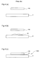
- FIGS. 4(a)-4(c) are diagrams illustrating a prior art die-bonding method of a semiconductor device.
- numeral 100 designates a semiconductor device which is cut into chip units from a wafer(not shown).
- the semiconductor device 100 comprises a single or a plurality of semiconductor elements formed on a semiconductor substrate.
- Numeral 4 designates a die-pad serving as a part of a package for sealing the semiconductor device 100, on which the semiconductor device 100 is fixed.
- Numeral 10 designates conductive paste comprising epoxy based resin (hereinafter referred to as epoxy based conductive paste), and this includes epoxy based resin, solvent, and conductive filler such as Ag.
- Numeral 1000 designates a die-bonded semiconductor device comprising the semiconductor device 100 being die-bonded on the die-pad 4.
- a semiconductor device 100 and a die-pad 4 are prepared.
- the epoxy based conductive paste 10 is plated to a position on the die-pad where the semiconductor device is to be fixed as shown in figure 4(b), then the semiconductor device 100 is disposed on this paste 10, and the entirety of these is inserted into a cure furnace.
- the curing is performed at a temperature of about 150°C, and the epoxy based conductive paste 10 is hardened to perform the die-bonding, whereby a die-bonded semiconductor device 1000 as shown in figure 4(c) is obtained.
- the epoxy based conductive paste 10 for each package with controlling the configuration of the epoxy based conductive paste 10 in accordance with the size of the semiconductor device, whereby the mounting method becomes complicated.
- the epoxy based conductive paste 10 crawls up to the surface along the side surface of the semiconductor device 100, and unrequired portions are conducted by the epoxy based conductive paste 10, thereby reducing the fabrication yield of the semiconductor device.
- the epoxy based conductive paste 10 includes solvent therein and when the curing is performed placing the semiconductor device 100 on the paste 10, the solvent in the paste 10 is evaporated. Therefore, it may happen that the semiconductor device 100 is corroded by the evaporated solvent. Or the solvent may be re-deposited on the wire bonding pad on the surface of the semiconductor substrate 100. In the latter case, no good wire bonding is performed in the later process.
- the solvent included in the epoxy based conductive paste 10 is likely to be evaporated at a room temperature. Therefore, it is difficult to keep the paste 10 at the room temperature.
- the wire bonding process is usually performed at a temperature of 200 °C, and the anti-heat temperature of epoxy based resin forming the epoxy based conductive paste 10 is low to be about 200 °C. Therefore, it may happen that the epoxy based resin of the paste 10 is dissociated in the wire-bonding process that is performed at the above-described temperature, and the surface of the semiconductor device 100 was contaminated.
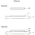
- Figures 5(a)-5(b) illustrate another prior art die-bonding method of a semiconductor device which can solve the problems in the prior art example described with reference to figures 4(a)-4(c), which is recited in, for example, Japanese Published Patent Application No.59-117240 and Japanese Published Patent Application No.1-272124.
- the same reference numerals designate the same or corresponding elements as in figure 4.
- Numeral 11 designates thermoplastic conductive paste. This paste 11 comprises thermoplastic resin, and this includes solvent, and particles comprising conductive material as fillers.
- numeral 11a designates a thermoplastic conductive resin layer which has made the solvent evaporated and has been hardened.
- the conductive paste 11 comprising thermoplastic resin layer is plated onto a portion on the die-pad 4 where a semiconductor device is to be adhered and this is heated to remove the solvent therein to form thermoplastic conductive resin layer 11a.
- the semiconductor device 100 is mounted thereon, and heating processing is performed to harden the thermoplastic conductive resin layer 11a, thereby bonding the die-pad 4 and the semiconductor device 100.
- thermoplastic conductive paste 1 comprising thermoplastic resin
- the semiconductor device would not be unfavorably affected by the gases which are generated by the evaporation of the solvent.
- the semiconductor device 100 is disposed on the thermoplastic conductive resin layer 11a which has been already hardened, differently from a case where the semiconductor device 100 is mounted on the paste shaped resin, the resin would not crawl up onto the upper surface from the side surface of the semiconductor device 100, thereby increasing the fabrication yield.
- thermoplastic resin would hardly deform after it is once plated on the die-pad 4 and hardened, its preservation and handling are quite easy. Further, since many thermoplastic resin have heat-resistant temperatures larger than 200 °C, it is possible to arise no dissociation and transformation in the high temperature processing in the later process such as wire bonding by increasing the heat-resistance temperature of the thermoplastic resin.
- Japanese Published Patent Application No.59-107528 and Japanese Published Patent Application No.60-52028 disclose methods in which a pellet or a ribbon comprising thermoplastic resin including Ag is put between by a die-pad and a semiconductor chip, and the thermoplastic resin pellet or ribbon is hardened by heat, thereby performing the die-bonding. Also by these methods, the problem in the prior art die-bonding method shown in figure 4 can be solved similarly as in the die-bonding method of a semiconductor device shown in figure 5.
- thermoplastic conductive resin layer or disposing such as a pellet comprising thermoplastic conductive resin for respective packages, and therefore, the work is complicated and the productivity is worse.
- the solvent included in the paste is evaporated after the paste is plated onto the die-pad, the surface of the die-pad, particularly, the surface of the metal pad used for such as wire-bonding would be contaminated by the gases obtained from the evaporation of the solvent, whereby the quality of the semiconductor device is deteriorated and the fabrication yield is lowered.
- a semiconductor device includes a semiconductor substrate having a first main surface; and a thermoplastic conductive resin layer comprising thermoplastic resin including particles comprising conductive material disposed on the first main surface of the semiconductor substrate. Therefore, positional deviation of the semiconductor device with a resin layer while die-bonding the semiconductor device is dispensed with, thereby increasing the fabrication yield.
- an apparatus and a process for disposing resin on a package can be omitted, thereby the die-bonding can be performed at a low cost.
- the semiconductor substrate has an element on a main surface opposite to the first main surface. Therefore, the positional deviation of the semiconductor device with the resin layer for die-bonding is dispensed with, and an apparatus and a process for disposing resin on a package during the die-bonding can be omitted.
- the conductive material comprises silver and the thermoplastic resin comprises thermoplastic polyimide. Therefore, adhesion with high heat-resisting property is performed.
- a fabricating method of a semiconductor device comprises: plating thermoplastic resin including particles comprising conductive material on a first main surface of a semiconductor substrate; and hardening the thermoplastic resin thereby to form a thin film thermoplastic conductive resin layer. Therefore, positional deviations of the semiconductor device with the resin layer while die-bonding the semiconductor device is dispensed with, thereby increasing the fabrication yield.
- an apparatus and a process for disposing resin on a package can be omitted, thereby the die-bonding can be performed at a low cost.
- the process of plating conductive resin comprises dropping thermoplastic resin including particles comprising conductive material, with rotating the semiconductor substrate in a plane parallel with the first main surface of the semiconductor substrate. Therefore, it is possible to form a uniform and thin thermoplastic resin film, thereby the heat conductivity between the semiconductor device and the die-pad is improved.
- the process of forming the thermoplastic conductive resin layer is performed by making the second main surface which is opposite to the first main surface of the semiconductor substrate adhere to a rotating plate which holds and rotates the semiconductor substrate without exposing its opposite first main surface to the external air. Therefore, the contaminations on the surface of the semiconductor device due to gases which are generated by the solvent included in the thermo-plastic resin material before the surface of the semiconductor device is hardened can be prevented.
- the semiconductor substrate is in a wafer shape and the method further includes, after forming the thermoplastic conductive resin layer, separating the wafer shape substrate into chips. Therefore, a plurality of semiconductor devices each provided with thermo-plastic conductive resin layer at its rear surface can be obtained at one time.
- the conductive material comprises silver and the thermoplastic resin comprises thermoplastic polyimide. Therefore, adhesion with high heat-resisting property is performed.
- a die-bonding method of a semiconductor device comprises: forming a semiconductor device comprising a semiconductor substrate having a first main surface and a thermoplastic conductive resin layer comprising thermoplastic resin including particles comprising conductive material disposed on the first main surface of the semiconductor substrate; holding a supporting member on which the semiconductor substrate is to be die-bonded, at a temperature higher than the glass transition temperature of the thermoplastic conductive resin layer; and applying pressure to the semiconductor device with making the first main surface of the semiconductor substrate on which the thermoplastic conductive resin layer is provided directed toward the supporting member to make the semiconductor device adhere to the supporting member. Therefore, the process of setting the resin layer on a mounting plate of the package for mounting a semiconductor device can be omitted, and the die-bonding process can be simplified, thereby enhancing the productivity.
- Figure 1 is a cross-sectional view illustrating a structure of a semiconductor device according to a first embodiment of the present invention.
- Figure 2 is a diagram for explaining the die-bonding method utilized in the fabricating method of a semiconductor device according to the first embodiment of the present invention.
- Figures 3(a)-3(e) are process diagrams illustrating a fabricating method of a semiconductor device according to a first embodiment of the present invention.
- Figures 4(a)-4(c) are diagrams illustrating a prior art die-bonding method of a semiconductor device.
- Figures 5(a)-5(b) are diagrams illustrating another prior art die-bonding method of a semiconductor device which can solve the problems in the prior art example described with reference to figures 4(a)-4(c).
- Figure 1 is a cross-sectional view illustrating a structure of a semiconductor device according to a first embodiment of the present invention.
- numeral 1a designates a semiconductor chip which is cut out from a wafer (not shown). This semiconductor chip comprises a single or a plurality of semiconductor elements formed on a semiconductor substrate.
- Numeral 7a designates a thermoplastic polyimide resin layer including particles comprising conductive material, disposed on the rear surface of the semiconductor chip 1a.
- the particles comprising conductive material silver particles in a scale shape having a thickness of 0.5 ⁇ 3 ⁇ m and having an area of several tens square ⁇ m, or silver particles in a spherical shape of a diameter of several ⁇ m are used, and the quantity thereof is adjusted as required.
- the resistance of the thermoplastic conductive polyimide resin layer 7a of this embodiment is 10 -4 ⁇ 10 -6 ⁇ cm, and the thermal conductivity thereof is 10 -3 ⁇ 10 -1 cal/cm ⁇ sec°C.
- Figure 2 is a diagram for explaining a die-bonding method utilized in the fabricating method of a semiconductor device according to the first embodiment of the present invention.
- the same reference numerals designate the same or corresponding elements.
- Numeral 2 designates a collet for moving the semiconductor device 1 which is absorbed to the collet 2 itself. This collet 2 is provided with a vacuum absorbing means for absorbing the semiconductor device 1.
- Numeral 3 designates a heat stage provided with a heating means inside thereof.
- Numeral 4 designates a die-pad serving as a part of the package sealing the semiconductor device 100. The semiconductor device 1 is adhered onto the die-pad 4.
- FIGS 3(a)-3(e) are process diagrams illustrating a fabricating method of a semiconductor device according to a first embodiment of the present invention.
- the same reference numerals designate the same or corresponding elements.
- Numeral 1b designates a semiconductor substrate in a wafer shape on which a plurality of elements (not shown in the figure) are disposed.
- Numeral 5 designates a glass plate.
- Numeral 15 designates a wax for fixing the semiconductor device.
- Numeral 6 designates a mounting plate of a spin coater (not shown) similar as that used in the usual photoresist plating process, and this plating plate 6 is rotatable in the horizontal direction and a vacuum absorbing means (not shown) for vacuum absorbing the wafer is provided on the surface.
- Numeral 7 designates thermoplastic conductive resin paste comprising the resin of the same material as the thermoplastic conductive polyimide resin layer 7a including the conductive material and the solvent.
- thermoplastic conductive polyimide resin paste 7 is dropped and it is made a uniform thin film by utilizing the centrifugal force, and it is heated and dried to obtain the thermoplastic conductive polyimide resin layer 7a on the rear surface of the wafer 1b (figure 3(d)). Thereafter, the wafer 1b which has the thermoplastic conductive polyimide resin layer 7a on its rear surface is removed from the glass plate 5 by melting the wax 15 (figure 3(e)).
- the surface of the wafer 1b which has the thermoplastic conductive polyimide resin layer 7a thereon is fixed to a UV (ultraviolet) tape (not shown) whose adhesion intensity is reduced by that the ultraviolet light is irradiated, and thereafter, the wafer 1b is separated into chips by dicing. Thereafter, ultraviolet light is irradiated to the UV tape thereby to reduce the adhesion, and the semiconductor devices are removed from the UV tape into respective separated chips, thereby obtaining the semiconductor devices 1 each provided with the thermoplastic conductive polyimide resin layer 7a on its surface.
- a UV (ultraviolet) tape not shown
- the die-bonding method of a semiconductor device will be described.
- the surface of the semiconductor substrate 1 which is opposite to the surface of the semiconductor device 1 on which the thermoplastic conductive polyimide resin layer 7a is provided is held absorbed by such as a collet 2.
- This is pressed to a position on the die-pad 4 where a semiconductor device is to be placed.
- This die-pad 4 is previously heated to a temperature a little higher than the glass transition temperature of thermoplastic conductive polyimide resin layer, for example, about 210°C for the resin layer having a glass transition temperature of 200°C.
- thermoplastic conductive polyimide resin layer 7a of the semiconductor device is softened by the heat of the die-pad 4, thereby die-bonding the semiconductor device 1 on the die-pad.
- the die-pad 4 is heated in this embodiment by a heating means provided inside the heat stage 3, but as a method for heating the die-pad 4, a high frequency heating or other method may be used.
- thermoplastic conductive polyimide resin layer 7a is provided on the surface of the substrate of the semiconductor device, there arises no positional deviation of the semiconductor device while attaching the semiconductor device to the die-pad 4 with relative to the thermoplastic conductive resin, and the die-bonding having the desired heat radiation property, conductivity, and intensity can be performed, and the fabrication yield can be enhanced.
- thermoplastic conductive resin layer and the semiconductor device have the same sizes, thereby providing no positional deviation with each other. Therefore, the size of the package can be made one that is minimized in accordance with the size of the semiconductor device.
- the fabricating apparatus can be simplified and the fabricating cost can be reduced. Further, since no processes are required to plate resin paste on respective packages mounting the semiconductor substrate or to dispose resin pellet, the fabricating process can be simplified and the productivity can be enhanced.
- thermoplastic conductive polyimide resin layer 7a can be formed to a uniform thickness and have a controlled thin thickness by a spin coating method, and therefore, the heat conductivity between the semiconductor chip 1a and the die-pad 1 after the die-bonding can be enhanced.
- thermoplastic conductive polyimide resin layer 7a is formed at the rear surface of the wafer 1b
- a plurality of semiconductor devices 1 each provided with the thermoplastic conductive polyimide resin layer 7a on its rear surface can be obtained at once, thereby increasing the productivity of semiconductor devices.
- thermoplastic resin is used as resin for die-bonding before the bonding of the semiconductor device 1, solvent is already evaporated from the thermoplastic conductive polyimide resin paste 7 similarly as in the other prior art. Therefore, the semiconductor device is not affected by the gases which are generated by the evaporation of the solvents. In addition, differently from the case where the semiconductor device 1 is fixed to the resin paste, the resin would not crawl up onto the upper surface from the side surface of the semiconductor device 1, thereby not deteriorating the fabrication yield. Further, since the thermoplastic resin would hardly transform after it is hardened, after it is plated onto the rear surface of the semiconductor device 1, the holding and handling thereof are easy. Further.
- the polyimide resin has thermal decomposition starting temperature of above 400 °C, no decomposition and deformation occur even at a high temperature processing in the later process such as the wire bonding, whereby the above-described problems as in the prior art die-bonding method are solved.
- thermoplastic conductive resin layer 7a is formed by using a spin coating method, since the surface of such as elements of the wafer 1b is sticked to the glass plate 5, the surface of the wafer 1b would not be contaminated by gasses which are generated by the evaporation of the solvent.
- thermoplastic conductive polyimide resin layer 7 since after the thermoplastic conductive polyimide resin layer 7 is formed on a rear surface of a wafer by spin coating method, and this is separated for respective elements, the semiconductor devices 1 each provided with the thermoplastic conductive polyimide resin layer 7a at its rear surface are obtained. Therefore, it is possible to make the positional deviation between the semiconductor device and the resin layer in the die-bonding process dispensed with and the die-bonding can be performed at a high yield. Accordingly, the apparatus and the process for plating resin paste can be omitted in the die-bonding process. Therefore, the fabricating apparatus and fabricating process are simplified, and the die-bonding can be performed at low cost and at high productivity.
- thermoplastic polyimide resin is employed as the thermoplastic resin
- the present invention can be applied to cases even when the other thermoplastic resin is used, and the same effects as in the above-described embodiment are obtained.
- thermoplastic resin having a glass transition temperature which is not softened by the high temperature processing.
- the thermoplastic conductive polyimide resin layer is formed on a wafer shaped semiconductor substrate on which a plurality of elements are formed by using a spin coating method, and thereafter, respective elements are cut out from the wafer to be the semiconductor devices.
- a wafer on which a lot of elements are formed may be used, and after the thermoplastic conductive polyimide resin layer 7a is formed thereon, the wafer may be used for die-bonding without cut out into respective chips.
- a semiconductor substrate on which no elements are formed may be used.
- thermoplastic conductive polyimide resin layer is formed on the surface of the substrate, elements are formed on the opposite surface thereof, and the wafer is cut out into chips or it may be used for the die-bonding as it is, with the same effects as described above.
Landscapes
- Die Bonding (AREA)
Applications Claiming Priority (2)
| Application Number | Priority Date | Filing Date | Title |
|---|---|---|---|
| JP39950/95 | 1995-02-28 | ||
| JP7039950A JPH08236554A (ja) | 1995-02-28 | 1995-02-28 | 半導体装置,及び半導体装置の製造方法,並びに半導体装置のダイボンディング方法 |
Publications (2)
| Publication Number | Publication Date |
|---|---|
| EP0730294A2 true EP0730294A2 (fr) | 1996-09-04 |
| EP0730294A3 EP0730294A3 (fr) | 1998-04-08 |
Family
ID=12567251
Family Applications (1)
| Application Number | Title | Priority Date | Filing Date |
|---|---|---|---|
| EP95118241A Withdrawn EP0730294A3 (fr) | 1995-02-28 | 1995-11-20 | Procédé de fabrication d'un dispositif semi-conducteur et procédé de montage d'un dispositif semi-conducteur |
Country Status (2)
| Country | Link |
|---|---|
| EP (1) | EP0730294A3 (fr) |
| JP (1) | JPH08236554A (fr) |
Cited By (1)
| Publication number | Priority date | Publication date | Assignee | Title |
|---|---|---|---|---|
| CN110920033A (zh) * | 2019-12-25 | 2020-03-27 | 雷誉(上海)包装制品有限公司 | 一种吸塑产品的吸塑成型工艺 |
Families Citing this family (4)
| Publication number | Priority date | Publication date | Assignee | Title |
|---|---|---|---|---|
| US6368890B1 (en) | 1999-05-05 | 2002-04-09 | Mitel Semiconductor Ab | Top contact VCSEL with monitor |
| JP2007048958A (ja) | 2005-08-10 | 2007-02-22 | Renesas Technology Corp | 半導体装置の製造方法および半導体装置 |
| JP5662706B2 (ja) * | 2010-06-08 | 2015-02-04 | 株式会社ディスコ | 液状樹脂の塗布装置 |
| JP2011009756A (ja) * | 2010-07-12 | 2011-01-13 | Asahi Kasei Electronics Co Ltd | 磁電変換素子の製造方法 |
Citations (4)
| Publication number | Priority date | Publication date | Assignee | Title |
|---|---|---|---|---|
| JPS59107528A (ja) | 1982-12-13 | 1984-06-21 | Hitachi Ltd | 半導体装置のダイボンデイング材料 |
| JPS59117240A (ja) | 1982-12-24 | 1984-07-06 | Hitachi Ltd | 半導体装置 |
| JPS6052028A (ja) | 1983-09-01 | 1985-03-23 | Hitachi Chem Co Ltd | 半導体装置の製造法 |
| JPH01272124A (ja) | 1988-04-25 | 1989-10-31 | Hitachi Ltd | 半導体装置の製造方法 |
Family Cites Families (7)
| Publication number | Priority date | Publication date | Assignee | Title |
|---|---|---|---|---|
| JPS5984532A (ja) * | 1982-11-08 | 1984-05-16 | Hitachi Ltd | 半導体装置の製造方法および半導体ウエ−ハ |
| JPS59200438A (ja) * | 1983-04-28 | 1984-11-13 | Oki Electric Ind Co Ltd | 半導体装置の製造方法 |
| IE55524B1 (en) * | 1983-06-13 | 1990-10-10 | Minnesota Mining & Mfg | Electrically and thermally conductive adhesive transfer tape |
| JPS6150344A (ja) * | 1984-08-18 | 1986-03-12 | Hitachi Chem Co Ltd | 集積回路の接続方法 |
| JPS62285429A (ja) * | 1986-06-04 | 1987-12-11 | Toshiba Chem Corp | 半導体装置の製造方法 |
| JPH01272125A (ja) * | 1988-04-22 | 1989-10-31 | Nitto Denko Corp | 半導体装置の製造方法 |
| JPH0715087B2 (ja) * | 1988-07-21 | 1995-02-22 | リンテック株式会社 | 粘接着テープおよびその使用方法 |
-
1995
- 1995-02-28 JP JP7039950A patent/JPH08236554A/ja active Pending
- 1995-11-20 EP EP95118241A patent/EP0730294A3/fr not_active Withdrawn
Patent Citations (4)
| Publication number | Priority date | Publication date | Assignee | Title |
|---|---|---|---|---|
| JPS59107528A (ja) | 1982-12-13 | 1984-06-21 | Hitachi Ltd | 半導体装置のダイボンデイング材料 |
| JPS59117240A (ja) | 1982-12-24 | 1984-07-06 | Hitachi Ltd | 半導体装置 |
| JPS6052028A (ja) | 1983-09-01 | 1985-03-23 | Hitachi Chem Co Ltd | 半導体装置の製造法 |
| JPH01272124A (ja) | 1988-04-25 | 1989-10-31 | Hitachi Ltd | 半導体装置の製造方法 |
Cited By (1)
| Publication number | Priority date | Publication date | Assignee | Title |
|---|---|---|---|---|
| CN110920033A (zh) * | 2019-12-25 | 2020-03-27 | 雷誉(上海)包装制品有限公司 | 一种吸塑产品的吸塑成型工艺 |
Also Published As
| Publication number | Publication date |
|---|---|
| JPH08236554A (ja) | 1996-09-13 |
| EP0730294A3 (fr) | 1998-04-08 |
Similar Documents
| Publication | Publication Date | Title |
|---|---|---|
| US7091109B2 (en) | Semiconductor device and method for producing the same by dicing | |
| US7969026B2 (en) | Flexible carrier for high volume electronic package fabrication | |
| KR100337412B1 (ko) | 저면보호막을가진반도체웨이퍼,집적회로디바이스및그제조방법 | |
| US5960260A (en) | Semiconductor device, its manufacturing method, and dicing adhesive element therefor | |
| KR100517075B1 (ko) | 반도체 소자 제조 방법 | |
| US20040097054A1 (en) | Fabrication method of semiconductor circuit device | |
| US7129118B2 (en) | Protective tape removing apparatus and method of assembling semiconductor package using the same | |
| JPH11512875A (ja) | リード変形を有する接続多重超小形電子素子 | |
| US5477081A (en) | Semiconductor device package | |
| US20070124928A1 (en) | Circuit substrates, semiconductor devices, semiconductor manufacturing apparatuses, methods for manufacturing circuit substrates, and methods for manufacturing semiconductor devices | |
| US7517722B2 (en) | Method of producing a universal semiconductor housing with precrosslinked plastic embedding compounds | |
| US7256074B2 (en) | Methods for wafer-level packaging of microelectronic devices and microelectronic devices formed by such methods | |
| JP3811567B2 (ja) | 半導体装置の製造方法 | |
| EP0338199B1 (fr) | Procédé et appareil pour encapsuler un dispositif électronique | |
| EP0730294A2 (fr) | Procédé de fabrication d'un dispositif semi-conducteur et procédé de montage d'un dispositif semi-conducteur | |
| JPH07263382A (ja) | ウェーハ固定用テープ | |
| JPH11163006A (ja) | ペレットボンディング方法 | |
| CN118263168A (zh) | 芯片贴装装置以及剥离夹具 | |
| US7528054B2 (en) | Semiconductor component with a thin semiconductor chip and a stiff wiring substrate, and methods for producing and further processing of thin semiconductor chips | |
| US20040262722A1 (en) | Chip mounting method and mounted substrate manufacturing apparatus | |
| JPH07302808A (ja) | 電子部材のコーティング方法 | |
| JP3381563B2 (ja) | 半導体装置の製造方法 | |
| EP0736225A1 (fr) | Procede de fixation de puces de circuit integre consistant a appliquer a l'aide d'un cylindre des adhesifs sur des tranches de semi-conducteurs | |
| US11329021B2 (en) | Method for fabricating a semiconductor device comprising a paste layer and semiconductor device | |
| CN1182282A (zh) | 片上引线式半导体芯片封装及其制作方法 |
Legal Events
| Date | Code | Title | Description |
|---|---|---|---|
| PUAI | Public reference made under article 153(3) epc to a published international application that has entered the european phase |
Free format text: ORIGINAL CODE: 0009012 |
|
| AK | Designated contracting states |
Kind code of ref document: A2 Designated state(s): DE FR GB |
|
| PUAL | Search report despatched |
Free format text: ORIGINAL CODE: 0009013 |
|
| AK | Designated contracting states |
Kind code of ref document: A3 Designated state(s): DE FR GB |
|
| STAA | Information on the status of an ep patent application or granted ep patent |
Free format text: STATUS: THE APPLICATION IS DEEMED TO BE WITHDRAWN |
|
| 18D | Application deemed to be withdrawn |
Effective date: 19990708 |