EP0747974A2 - Photovoltaisches Bauelement und Herstellungsverfahren - Google Patents
Photovoltaisches Bauelement und Herstellungsverfahren Download PDFInfo
- Publication number
- EP0747974A2 EP0747974A2 EP96108498A EP96108498A EP0747974A2 EP 0747974 A2 EP0747974 A2 EP 0747974A2 EP 96108498 A EP96108498 A EP 96108498A EP 96108498 A EP96108498 A EP 96108498A EP 0747974 A2 EP0747974 A2 EP 0747974A2
- Authority
- EP
- European Patent Office
- Prior art keywords
- layer
- type
- gas
- type semiconductor
- semiconductor layer
- Prior art date
- Legal status (The legal status is an assumption and is not a legal conclusion. Google has not performed a legal analysis and makes no representation as to the accuracy of the status listed.)
- Withdrawn
Links
- 238000000034 method Methods 0.000 title claims abstract description 222
- 230000008569 process Effects 0.000 title claims abstract description 157
- 238000004519 manufacturing process Methods 0.000 title claims abstract description 74
- 239000004065 semiconductor Substances 0.000 claims abstract description 806
- 239000000470 constituent Substances 0.000 claims abstract description 47
- 239000013078 crystal Substances 0.000 claims abstract description 35
- 239000007789 gas Substances 0.000 claims description 1039
- 238000000151 deposition Methods 0.000 claims description 621
- 239000000758 substrate Substances 0.000 claims description 534
- 239000003795 chemical substances by application Substances 0.000 claims description 104
- 238000010790 dilution Methods 0.000 claims description 28
- 239000012895 dilution Substances 0.000 claims description 28
- 229910052739 hydrogen Inorganic materials 0.000 claims description 22
- 239000001257 hydrogen Substances 0.000 claims description 19
- 125000004435 hydrogen atom Chemical group [H]* 0.000 claims description 17
- IJGRMHOSHXDMSA-UHFFFAOYSA-N Atomic nitrogen Chemical compound N#N IJGRMHOSHXDMSA-UHFFFAOYSA-N 0.000 claims description 16
- UFHFLCQGNIYNRP-UHFFFAOYSA-N Hydrogen Chemical compound [H][H] UFHFLCQGNIYNRP-UHFFFAOYSA-N 0.000 claims description 15
- 229910052710 silicon Inorganic materials 0.000 claims description 13
- 125000004429 atom Chemical group 0.000 claims description 11
- 229910052799 carbon Inorganic materials 0.000 claims description 10
- 230000000737 periodic effect Effects 0.000 claims description 10
- 239000010703 silicon Substances 0.000 claims description 9
- QVGXLLKOCUKJST-UHFFFAOYSA-N atomic oxygen Chemical compound [O] QVGXLLKOCUKJST-UHFFFAOYSA-N 0.000 claims description 8
- 229910052757 nitrogen Inorganic materials 0.000 claims description 8
- 229910052760 oxygen Inorganic materials 0.000 claims description 8
- 239000001301 oxygen Substances 0.000 claims description 8
- OKTJSMMVPCPJKN-UHFFFAOYSA-N Carbon Chemical compound [C] OKTJSMMVPCPJKN-UHFFFAOYSA-N 0.000 claims description 7
- 150000002431 hydrogen Chemical class 0.000 claims description 7
- 239000012298 atmosphere Substances 0.000 claims description 4
- 229910052732 germanium Inorganic materials 0.000 claims description 4
- GNPVGFCGXDBREM-UHFFFAOYSA-N germanium atom Chemical compound [Ge] GNPVGFCGXDBREM-UHFFFAOYSA-N 0.000 claims description 4
- 238000006243 chemical reaction Methods 0.000 abstract description 163
- 239000010410 layer Substances 0.000 description 2535
- 230000008021 deposition Effects 0.000 description 584
- 230000015572 biosynthetic process Effects 0.000 description 256
- BLRPTPMANUNPDV-UHFFFAOYSA-N Silane Chemical compound [SiH4] BLRPTPMANUNPDV-UHFFFAOYSA-N 0.000 description 179
- 229910021417 amorphous silicon Inorganic materials 0.000 description 141
- 238000010438 heat treatment Methods 0.000 description 114
- 239000010408 film Substances 0.000 description 105
- 230000001276 controlling effect Effects 0.000 description 96
- 238000005268 plasma chemical vapour deposition Methods 0.000 description 70
- 238000011156 evaluation Methods 0.000 description 64
- 238000012360 testing method Methods 0.000 description 64
- XYFCBTPGUUZFHI-UHFFFAOYSA-N Phosphine Chemical class P XYFCBTPGUUZFHI-UHFFFAOYSA-N 0.000 description 61
- 239000000463 material Substances 0.000 description 58
- 230000000052 comparative effect Effects 0.000 description 57
- 229910007264 Si2H6 Inorganic materials 0.000 description 50
- PZPGRFITIJYNEJ-UHFFFAOYSA-N disilane Chemical compound [SiH3][SiH3] PZPGRFITIJYNEJ-UHFFFAOYSA-N 0.000 description 50
- 239000006185 dispersion Substances 0.000 description 47
- 229910021424 microcrystalline silicon Inorganic materials 0.000 description 42
- 229910000577 Silicon-germanium Inorganic materials 0.000 description 38
- 238000005019 vapor deposition process Methods 0.000 description 36
- QUZPNFFHZPRKJD-UHFFFAOYSA-N germane Chemical compound [GeH4] QUZPNFFHZPRKJD-UHFFFAOYSA-N 0.000 description 35
- 229910052986 germanium hydride Inorganic materials 0.000 description 35
- 239000011651 chromium Substances 0.000 description 25
- 229910045601 alloy Inorganic materials 0.000 description 22
- 239000000956 alloy Substances 0.000 description 22
- 238000005259 measurement Methods 0.000 description 21
- 229910052751 metal Inorganic materials 0.000 description 21
- 239000012535 impurity Substances 0.000 description 20
- 239000002184 metal Substances 0.000 description 20
- XLOMVQKBTHCTTD-UHFFFAOYSA-N Zinc monoxide Chemical compound [Zn]=O XLOMVQKBTHCTTD-UHFFFAOYSA-N 0.000 description 18
- 229910010271 silicon carbide Inorganic materials 0.000 description 18
- 230000003247 decreasing effect Effects 0.000 description 17
- 230000001965 increasing effect Effects 0.000 description 17
- 230000007423 decrease Effects 0.000 description 16
- 150000002500 ions Chemical class 0.000 description 16
- 150000001875 compounds Chemical class 0.000 description 13
- 229910001220 stainless steel Inorganic materials 0.000 description 13
- 239000010935 stainless steel Substances 0.000 description 13
- 230000004913 activation Effects 0.000 description 12
- 125000005843 halogen group Chemical group 0.000 description 12
- 239000000203 mixture Substances 0.000 description 12
- -1 polyethylene Polymers 0.000 description 12
- XUIMIQQOPSSXEZ-UHFFFAOYSA-N Silicon Chemical compound [Si] XUIMIQQOPSSXEZ-UHFFFAOYSA-N 0.000 description 11
- 238000004544 sputter deposition Methods 0.000 description 11
- 238000010521 absorption reaction Methods 0.000 description 10
- 229910052782 aluminium Inorganic materials 0.000 description 10
- 230000006872 improvement Effects 0.000 description 10
- HBMJWWWQQXIZIP-UHFFFAOYSA-N silicon carbide Chemical compound [Si+]#[C-] HBMJWWWQQXIZIP-UHFFFAOYSA-N 0.000 description 10
- 230000007547 defect Effects 0.000 description 9
- 238000002347 injection Methods 0.000 description 9
- 239000007924 injection Substances 0.000 description 9
- 230000031700 light absorption Effects 0.000 description 9
- 239000010409 thin film Substances 0.000 description 9
- 239000011787 zinc oxide Substances 0.000 description 9
- CSCPPACGZOOCGX-UHFFFAOYSA-N Acetone Chemical compound CC(C)=O CSCPPACGZOOCGX-UHFFFAOYSA-N 0.000 description 8
- KFZMGEQAYNKOFK-UHFFFAOYSA-N Isopropanol Chemical compound CC(C)O KFZMGEQAYNKOFK-UHFFFAOYSA-N 0.000 description 8
- LEVVHYCKPQWKOP-UHFFFAOYSA-N [Si].[Ge] Chemical compound [Si].[Ge] LEVVHYCKPQWKOP-UHFFFAOYSA-N 0.000 description 8
- 239000000969 carrier Substances 0.000 description 8
- XEEYBQQBJWHFJM-UHFFFAOYSA-N iron Substances [Fe] XEEYBQQBJWHFJM-UHFFFAOYSA-N 0.000 description 8
- XOLBLPGZBRYERU-UHFFFAOYSA-N tin dioxide Chemical compound O=[Sn]=O XOLBLPGZBRYERU-UHFFFAOYSA-N 0.000 description 8
- 241000511976 Hoya Species 0.000 description 7
- 229910017875 a-SiN Inorganic materials 0.000 description 7
- 239000010949 copper Substances 0.000 description 7
- 238000009792 diffusion process Methods 0.000 description 7
- 230000000694 effects Effects 0.000 description 7
- 238000005468 ion implantation Methods 0.000 description 7
- 150000002739 metals Chemical class 0.000 description 7
- 238000002360 preparation method Methods 0.000 description 7
- 239000000126 substance Substances 0.000 description 7
- 229910003811 SiGeC Inorganic materials 0.000 description 6
- 239000000370 acceptor Substances 0.000 description 6
- 229910052796 boron Inorganic materials 0.000 description 6
- 229910052802 copper Inorganic materials 0.000 description 6
- NEPLKJAINOWIJL-DHNNRRLOSA-N dnc014884 Polymers C1C2=CC3=CC=CC=C3N2[C@@]2(C)[C@@H]1[C@@]1(C)CCC(=O)C(C)(C)[C@@H]1CC2 NEPLKJAINOWIJL-DHNNRRLOSA-N 0.000 description 6
- 230000002708 enhancing effect Effects 0.000 description 6
- 230000007246 mechanism Effects 0.000 description 6
- PXHVJJICTQNCMI-UHFFFAOYSA-N nickel Substances [Ni] PXHVJJICTQNCMI-UHFFFAOYSA-N 0.000 description 6
- 230000003287 optical effect Effects 0.000 description 6
- 238000007747 plating Methods 0.000 description 6
- 229910052814 silicon oxide Inorganic materials 0.000 description 6
- 238000007740 vapor deposition Methods 0.000 description 6
- 238000004804 winding Methods 0.000 description 6
- 229910006160 GeF4 Inorganic materials 0.000 description 5
- 229910004016 SiF2 Inorganic materials 0.000 description 5
- 229910004014 SiF4 Inorganic materials 0.000 description 5
- 229910052804 chromium Inorganic materials 0.000 description 5
- 229910052737 gold Inorganic materials 0.000 description 5
- 239000010931 gold Substances 0.000 description 5
- 229910052742 iron Inorganic materials 0.000 description 5
- 238000010248 power generation Methods 0.000 description 5
- 238000005096 rolling process Methods 0.000 description 5
- ABTOQLMXBSRXSM-UHFFFAOYSA-N silicon tetrafluoride Chemical compound F[Si](F)(F)F ABTOQLMXBSRXSM-UHFFFAOYSA-N 0.000 description 5
- 229910052709 silver Inorganic materials 0.000 description 5
- 239000007858 starting material Substances 0.000 description 5
- PPMWWXLUCOODDK-UHFFFAOYSA-N tetrafluorogermane Chemical compound F[Ge](F)(F)F PPMWWXLUCOODDK-UHFFFAOYSA-N 0.000 description 5
- XXZCIYUJYUESMD-UHFFFAOYSA-N 2-[4-[2-(2,3-dihydro-1H-inden-2-ylamino)pyrimidin-5-yl]-3-(morpholin-4-ylmethyl)pyrazol-1-yl]-1-(2,4,6,7-tetrahydrotriazolo[4,5-c]pyridin-5-yl)ethanone Chemical compound C1C(CC2=CC=CC=C12)NC1=NC=C(C=N1)C=1C(=NN(C=1)CC(=O)N1CC2=C(CC1)NN=N2)CN1CCOCC1 XXZCIYUJYUESMD-UHFFFAOYSA-N 0.000 description 4
- RYGMFSIKBFXOCR-UHFFFAOYSA-N Copper Chemical compound [Cu] RYGMFSIKBFXOCR-UHFFFAOYSA-N 0.000 description 4
- VYPSYNLAJGMNEJ-UHFFFAOYSA-N Silicium dioxide Chemical compound O=[Si]=O VYPSYNLAJGMNEJ-UHFFFAOYSA-N 0.000 description 4
- XAGFODPZIPBFFR-UHFFFAOYSA-N aluminium Chemical compound [Al] XAGFODPZIPBFFR-UHFFFAOYSA-N 0.000 description 4
- 229910052787 antimony Inorganic materials 0.000 description 4
- 239000002131 composite material Substances 0.000 description 4
- 239000000835 fiber Substances 0.000 description 4
- 229910052738 indium Inorganic materials 0.000 description 4
- PJXISJQVUVHSOJ-UHFFFAOYSA-N indium(III) oxide Inorganic materials [O-2].[O-2].[O-2].[In+3].[In+3] PJXISJQVUVHSOJ-UHFFFAOYSA-N 0.000 description 4
- 229910052750 molybdenum Inorganic materials 0.000 description 4
- 229910021421 monocrystalline silicon Inorganic materials 0.000 description 4
- 229910052759 nickel Inorganic materials 0.000 description 4
- 229910052698 phosphorus Inorganic materials 0.000 description 4
- 238000002310 reflectometry Methods 0.000 description 4
- 238000000926 separation method Methods 0.000 description 4
- 239000010936 titanium Substances 0.000 description 4
- 229910052719 titanium Inorganic materials 0.000 description 4
- YJLUBHOZZTYQIP-UHFFFAOYSA-N 2-[5-[2-(2,3-dihydro-1H-inden-2-ylamino)pyrimidin-5-yl]-1,3,4-oxadiazol-2-yl]-1-(2,4,6,7-tetrahydrotriazolo[4,5-c]pyridin-5-yl)ethanone Chemical compound C1C(CC2=CC=CC=C12)NC1=NC=C(C=N1)C1=NN=C(O1)CC(=O)N1CC2=C(CC1)NN=N2 YJLUBHOZZTYQIP-UHFFFAOYSA-N 0.000 description 3
- ZOXJGFHDIHLPTG-UHFFFAOYSA-N Boron Chemical compound [B] ZOXJGFHDIHLPTG-UHFFFAOYSA-N 0.000 description 3
- OZJHCMYAXLCFKU-UHFFFAOYSA-N Polyavolensinone Natural products CC1(C)C2CCC3n4c(CC3(C)C2(C)CCC1=O)cc5ccccc45 OZJHCMYAXLCFKU-UHFFFAOYSA-N 0.000 description 3
- BQCADISMDOOEFD-UHFFFAOYSA-N Silver Chemical compound [Ag] BQCADISMDOOEFD-UHFFFAOYSA-N 0.000 description 3
- 230000009471 action Effects 0.000 description 3
- PNEYBMLMFCGWSK-UHFFFAOYSA-N aluminium oxide Inorganic materials [O-2].[O-2].[O-2].[Al+3].[Al+3] PNEYBMLMFCGWSK-UHFFFAOYSA-N 0.000 description 3
- 229910052785 arsenic Inorganic materials 0.000 description 3
- MGNHOGAVECORPT-UHFFFAOYSA-N difluorosilicon Chemical compound F[Si]F MGNHOGAVECORPT-UHFFFAOYSA-N 0.000 description 3
- 238000009826 distribution Methods 0.000 description 3
- 229910052731 fluorine Inorganic materials 0.000 description 3
- 229910052733 gallium Inorganic materials 0.000 description 3
- PCHJSUWPFVWCPO-UHFFFAOYSA-N gold Chemical compound [Au] PCHJSUWPFVWCPO-UHFFFAOYSA-N 0.000 description 3
- 230000033001 locomotion Effects 0.000 description 3
- 239000013081 microcrystal Substances 0.000 description 3
- 239000013080 microcrystalline material Substances 0.000 description 3
- 229910021420 polycrystalline silicon Inorganic materials 0.000 description 3
- 238000007639 printing Methods 0.000 description 3
- 239000004332 silver Substances 0.000 description 3
- 229910052715 tantalum Inorganic materials 0.000 description 3
- 229910052716 thallium Inorganic materials 0.000 description 3
- 229910052721 tungsten Inorganic materials 0.000 description 3
- 235000012431 wafers Nutrition 0.000 description 3
- HMUNWXXNJPVALC-UHFFFAOYSA-N 1-[4-[2-(2,3-dihydro-1H-inden-2-ylamino)pyrimidin-5-yl]piperazin-1-yl]-2-(2,4,6,7-tetrahydrotriazolo[4,5-c]pyridin-5-yl)ethanone Chemical compound C1C(CC2=CC=CC=C12)NC1=NC=C(C=N1)N1CCN(CC1)C(CN1CC2=C(CC1)NN=N2)=O HMUNWXXNJPVALC-UHFFFAOYSA-N 0.000 description 2
- VZSRBBMJRBPUNF-UHFFFAOYSA-N 2-(2,3-dihydro-1H-inden-2-ylamino)-N-[3-oxo-3-(2,4,6,7-tetrahydrotriazolo[4,5-c]pyridin-5-yl)propyl]pyrimidine-5-carboxamide Chemical compound C1C(CC2=CC=CC=C12)NC1=NC=C(C=N1)C(=O)NCCC(N1CC2=C(CC1)NN=N2)=O VZSRBBMJRBPUNF-UHFFFAOYSA-N 0.000 description 2
- SXAMGRAIZSSWIH-UHFFFAOYSA-N 2-[3-[2-(2,3-dihydro-1H-inden-2-ylamino)pyrimidin-5-yl]-1,2,4-oxadiazol-5-yl]-1-(2,4,6,7-tetrahydrotriazolo[4,5-c]pyridin-5-yl)ethanone Chemical compound C1C(CC2=CC=CC=C12)NC1=NC=C(C=N1)C1=NOC(=N1)CC(=O)N1CC2=C(CC1)NN=N2 SXAMGRAIZSSWIH-UHFFFAOYSA-N 0.000 description 2
- FYELSNVLZVIGTI-UHFFFAOYSA-N 2-[4-[2-(2,3-dihydro-1H-inden-2-ylamino)pyrimidin-5-yl]-5-ethylpyrazol-1-yl]-1-(2,4,6,7-tetrahydrotriazolo[4,5-c]pyridin-5-yl)ethanone Chemical compound C1C(CC2=CC=CC=C12)NC1=NC=C(C=N1)C=1C=NN(C=1CC)CC(=O)N1CC2=C(CC1)NN=N2 FYELSNVLZVIGTI-UHFFFAOYSA-N 0.000 description 2
- WZFUQSJFWNHZHM-UHFFFAOYSA-N 2-[4-[2-(2,3-dihydro-1H-inden-2-ylamino)pyrimidin-5-yl]piperazin-1-yl]-1-(2,4,6,7-tetrahydrotriazolo[4,5-c]pyridin-5-yl)ethanone Chemical compound C1C(CC2=CC=CC=C12)NC1=NC=C(C=N1)N1CCN(CC1)CC(=O)N1CC2=C(CC1)NN=N2 WZFUQSJFWNHZHM-UHFFFAOYSA-N 0.000 description 2
- CONKBQPVFMXDOV-QHCPKHFHSA-N 6-[(5S)-5-[[4-[2-(2,3-dihydro-1H-inden-2-ylamino)pyrimidin-5-yl]piperazin-1-yl]methyl]-2-oxo-1,3-oxazolidin-3-yl]-3H-1,3-benzoxazol-2-one Chemical compound C1C(CC2=CC=CC=C12)NC1=NC=C(C=N1)N1CCN(CC1)C[C@H]1CN(C(O1)=O)C1=CC2=C(NC(O2)=O)C=C1 CONKBQPVFMXDOV-QHCPKHFHSA-N 0.000 description 2
- 229910017083 AlN Inorganic materials 0.000 description 2
- 229910001369 Brass Inorganic materials 0.000 description 2
- 229920000049 Carbon (fiber) Polymers 0.000 description 2
- VYZAMTAEIAYCRO-UHFFFAOYSA-N Chromium Chemical compound [Cr] VYZAMTAEIAYCRO-UHFFFAOYSA-N 0.000 description 2
- 239000004593 Epoxy Substances 0.000 description 2
- ZOKXTWBITQBERF-UHFFFAOYSA-N Molybdenum Chemical compound [Mo] ZOKXTWBITQBERF-UHFFFAOYSA-N 0.000 description 2
- 239000004952 Polyamide Substances 0.000 description 2
- 239000004642 Polyimide Substances 0.000 description 2
- 229910052581 Si3N4 Inorganic materials 0.000 description 2
- GWEVSGVZZGPLCZ-UHFFFAOYSA-N Titan oxide Chemical compound O=[Ti]=O GWEVSGVZZGPLCZ-UHFFFAOYSA-N 0.000 description 2
- RTAQQCXQSZGOHL-UHFFFAOYSA-N Titanium Chemical compound [Ti] RTAQQCXQSZGOHL-UHFFFAOYSA-N 0.000 description 2
- QCWXUUIWCKQGHC-UHFFFAOYSA-N Zirconium Chemical compound [Zr] QCWXUUIWCKQGHC-UHFFFAOYSA-N 0.000 description 2
- 239000000654 additive Substances 0.000 description 2
- 230000000996 additive effect Effects 0.000 description 2
- VSCWAEJMTAWNJL-UHFFFAOYSA-K aluminium trichloride Chemical compound Cl[Al](Cl)Cl VSCWAEJMTAWNJL-UHFFFAOYSA-K 0.000 description 2
- 229910052797 bismuth Inorganic materials 0.000 description 2
- WMWLMWRWZQELOS-UHFFFAOYSA-N bismuth(iii) oxide Chemical compound O=[Bi]O[Bi]=O WMWLMWRWZQELOS-UHFFFAOYSA-N 0.000 description 2
- 239000010951 brass Substances 0.000 description 2
- 150000001721 carbon Chemical group 0.000 description 2
- 239000004917 carbon fiber Substances 0.000 description 2
- 239000000919 ceramic Substances 0.000 description 2
- 239000010941 cobalt Substances 0.000 description 2
- 229910017052 cobalt Inorganic materials 0.000 description 2
- GUTLYIVDDKVIGB-UHFFFAOYSA-N cobalt atom Chemical compound [Co] GUTLYIVDDKVIGB-UHFFFAOYSA-N 0.000 description 2
- 229910052681 coesite Inorganic materials 0.000 description 2
- 229910052593 corundum Inorganic materials 0.000 description 2
- 229910052906 cristobalite Inorganic materials 0.000 description 2
- KBDJQNUZLNUGDS-UHFFFAOYSA-N dibromosilicon Chemical compound Br[Si]Br KBDJQNUZLNUGDS-UHFFFAOYSA-N 0.000 description 2
- 239000002019 doping agent Substances 0.000 description 2
- 230000005684 electric field Effects 0.000 description 2
- 238000005516 engineering process Methods 0.000 description 2
- 238000002474 experimental method Methods 0.000 description 2
- 239000003365 glass fiber Substances 0.000 description 2
- PSCMQHVBLHHWTO-UHFFFAOYSA-K indium(iii) chloride Chemical compound Cl[In](Cl)Cl PSCMQHVBLHHWTO-UHFFFAOYSA-K 0.000 description 2
- 239000011733 molybdenum Substances 0.000 description 2
- JKQOBWVOAYFWKG-UHFFFAOYSA-N molybdenum trioxide Chemical compound O=[Mo](=O)=O JKQOBWVOAYFWKG-UHFFFAOYSA-N 0.000 description 2
- 229910052758 niobium Inorganic materials 0.000 description 2
- 239000010955 niobium Substances 0.000 description 2
- GUCVJGMIXFAOAE-UHFFFAOYSA-N niobium atom Chemical compound [Nb] GUCVJGMIXFAOAE-UHFFFAOYSA-N 0.000 description 2
- 229910052697 platinum Inorganic materials 0.000 description 2
- BASFCYQUMIYNBI-UHFFFAOYSA-N platinum Substances [Pt] BASFCYQUMIYNBI-UHFFFAOYSA-N 0.000 description 2
- 229920002647 polyamide Polymers 0.000 description 2
- 229920001721 polyimide Polymers 0.000 description 2
- 238000011160 research Methods 0.000 description 2
- 229920005989 resin Polymers 0.000 description 2
- 239000011347 resin Substances 0.000 description 2
- 239000000377 silicon dioxide Substances 0.000 description 2
- 238000001228 spectrum Methods 0.000 description 2
- 238000005507 spraying Methods 0.000 description 2
- 229910052682 stishovite Inorganic materials 0.000 description 2
- 229920003002 synthetic resin Polymers 0.000 description 2
- 239000000057 synthetic resin Substances 0.000 description 2
- GUVRBAGPIYLISA-UHFFFAOYSA-N tantalum atom Chemical compound [Ta] GUVRBAGPIYLISA-UHFFFAOYSA-N 0.000 description 2
- 230000007704 transition Effects 0.000 description 2
- 238000002834 transmittance Methods 0.000 description 2
- 229910052905 tridymite Inorganic materials 0.000 description 2
- WFKWXMTUELFFGS-UHFFFAOYSA-N tungsten Chemical compound [W] WFKWXMTUELFFGS-UHFFFAOYSA-N 0.000 description 2
- 239000010937 tungsten Substances 0.000 description 2
- 229910052720 vanadium Inorganic materials 0.000 description 2
- 229910001845 yogo sapphire Inorganic materials 0.000 description 2
- 229910052726 zirconium Inorganic materials 0.000 description 2
- 229910021630 Antimony pentafluoride Inorganic materials 0.000 description 1
- 229910017011 AsBr3 Inorganic materials 0.000 description 1
- 229910017009 AsCl3 Inorganic materials 0.000 description 1
- 229910017050 AsF3 Inorganic materials 0.000 description 1
- 229910017049 AsF5 Inorganic materials 0.000 description 1
- 229910015844 BCl3 Inorganic materials 0.000 description 1
- LFQSCWFLJHTTHZ-UHFFFAOYSA-N Ethanol Chemical compound CCO LFQSCWFLJHTTHZ-UHFFFAOYSA-N 0.000 description 1
- 229910005267 GaCl3 Inorganic materials 0.000 description 1
- 229910001218 Gallium arsenide Inorganic materials 0.000 description 1
- 229910006158 GeF2 Inorganic materials 0.000 description 1
- OKKJLVBELUTLKV-UHFFFAOYSA-N Methanol Chemical compound OC OKKJLVBELUTLKV-UHFFFAOYSA-N 0.000 description 1
- JCXJVPUVTGWSNB-UHFFFAOYSA-N Nitrogen dioxide Chemical compound O=[N]=O JCXJVPUVTGWSNB-UHFFFAOYSA-N 0.000 description 1
- GQPLMRYTRLFLPF-UHFFFAOYSA-N Nitrous Oxide Chemical compound [O-][N+]#N GQPLMRYTRLFLPF-UHFFFAOYSA-N 0.000 description 1
- 229910020667 PBr3 Inorganic materials 0.000 description 1
- 229910020656 PBr5 Inorganic materials 0.000 description 1
- 239000004698 Polyethylene Substances 0.000 description 1
- 239000004743 Polypropylene Substances 0.000 description 1
- 239000004793 Polystyrene Substances 0.000 description 1
- 229920001328 Polyvinylidene chloride Polymers 0.000 description 1
- 229910007245 Si2Cl6 Inorganic materials 0.000 description 1
- 229910007260 Si2F6 Inorganic materials 0.000 description 1
- 229910005096 Si3H8 Inorganic materials 0.000 description 1
- 229910003676 SiBr4 Inorganic materials 0.000 description 1
- 229910003910 SiCl4 Inorganic materials 0.000 description 1
- 229910003818 SiH2Cl2 Inorganic materials 0.000 description 1
- 229910003828 SiH3 Inorganic materials 0.000 description 1
- 229910003822 SiHCl3 Inorganic materials 0.000 description 1
- 229910020328 SiSn Inorganic materials 0.000 description 1
- 230000001133 acceleration Effects 0.000 description 1
- 229910000074 antimony hydride Inorganic materials 0.000 description 1
- VBVBHWZYQGJZLR-UHFFFAOYSA-I antimony pentafluoride Chemical compound F[Sb](F)(F)(F)F VBVBHWZYQGJZLR-UHFFFAOYSA-I 0.000 description 1
- FAPDDOBMIUGHIN-UHFFFAOYSA-K antimony trichloride Chemical compound Cl[Sb](Cl)Cl FAPDDOBMIUGHIN-UHFFFAOYSA-K 0.000 description 1
- GUNJVIDCYZYFGV-UHFFFAOYSA-K antimony trifluoride Chemical compound F[Sb](F)F GUNJVIDCYZYFGV-UHFFFAOYSA-K 0.000 description 1
- VMPVEPPRYRXYNP-UHFFFAOYSA-I antimony(5+);pentachloride Chemical compound Cl[Sb](Cl)(Cl)(Cl)Cl VMPVEPPRYRXYNP-UHFFFAOYSA-I 0.000 description 1
- 229910052786 argon Inorganic materials 0.000 description 1
- RBFQJDQYXXHULB-UHFFFAOYSA-N arsane Chemical compound [AsH3] RBFQJDQYXXHULB-UHFFFAOYSA-N 0.000 description 1
- 229910000070 arsenic hydride Inorganic materials 0.000 description 1
- YBGKQGSCGDNZIB-UHFFFAOYSA-N arsenic pentafluoride Chemical compound F[As](F)(F)(F)F YBGKQGSCGDNZIB-UHFFFAOYSA-N 0.000 description 1
- JMBNQWNFNACVCB-UHFFFAOYSA-N arsenic tribromide Chemical compound Br[As](Br)Br JMBNQWNFNACVCB-UHFFFAOYSA-N 0.000 description 1
- OEYOHULQRFXULB-UHFFFAOYSA-N arsenic trichloride Chemical compound Cl[As](Cl)Cl OEYOHULQRFXULB-UHFFFAOYSA-N 0.000 description 1
- JCMGUODNZMETBM-UHFFFAOYSA-N arsenic trifluoride Chemical compound F[As](F)F JCMGUODNZMETBM-UHFFFAOYSA-N 0.000 description 1
- 230000008901 benefit Effects 0.000 description 1
- JHXKRIRFYBPWGE-UHFFFAOYSA-K bismuth chloride Chemical compound Cl[Bi](Cl)Cl JHXKRIRFYBPWGE-UHFFFAOYSA-K 0.000 description 1
- 229910000072 bismuth hydride Inorganic materials 0.000 description 1
- TXKAQZRUJUNDHI-UHFFFAOYSA-K bismuth tribromide Chemical compound Br[Bi](Br)Br TXKAQZRUJUNDHI-UHFFFAOYSA-K 0.000 description 1
- BPBOBPIKWGUSQG-UHFFFAOYSA-N bismuthane Chemical compound [BiH3] BPBOBPIKWGUSQG-UHFFFAOYSA-N 0.000 description 1
- UORVGPXVDQYIDP-UHFFFAOYSA-N borane Chemical class B UORVGPXVDQYIDP-UHFFFAOYSA-N 0.000 description 1
- 229910052794 bromium Inorganic materials 0.000 description 1
- 229920002301 cellulose acetate Polymers 0.000 description 1
- 229910052801 chlorine Inorganic materials 0.000 description 1
- 239000003245 coal Substances 0.000 description 1
- 239000011248 coating agent Substances 0.000 description 1
- 238000000576 coating method Methods 0.000 description 1
- 238000004891 communication Methods 0.000 description 1
- 238000002109 crystal growth method Methods 0.000 description 1
- 230000000593 degrading effect Effects 0.000 description 1
- 230000006866 deterioration Effects 0.000 description 1
- 230000002542 deteriorative effect Effects 0.000 description 1
- BUMGIEFFCMBQDG-UHFFFAOYSA-N dichlorosilicon Chemical compound Cl[Si]Cl BUMGIEFFCMBQDG-UHFFFAOYSA-N 0.000 description 1
- VURFVHCLMJOLKN-UHFFFAOYSA-N diphosphane Chemical compound PP VURFVHCLMJOLKN-UHFFFAOYSA-N 0.000 description 1
- 238000007598 dipping method Methods 0.000 description 1
- 238000001312 dry etching Methods 0.000 description 1
- 238000005530 etching Methods 0.000 description 1
- 239000002803 fossil fuel Substances 0.000 description 1
- UPWPDUACHOATKO-UHFFFAOYSA-K gallium trichloride Chemical compound Cl[Ga](Cl)Cl UPWPDUACHOATKO-UHFFFAOYSA-K 0.000 description 1
- VGRFVJMYCCLWPQ-UHFFFAOYSA-N germanium Chemical compound [Ge].[Ge] VGRFVJMYCCLWPQ-UHFFFAOYSA-N 0.000 description 1
- 239000011521 glass Substances 0.000 description 1
- 229910052736 halogen Inorganic materials 0.000 description 1
- 150000002367 halogens Chemical class 0.000 description 1
- 229920006015 heat resistant resin Polymers 0.000 description 1
- 229910052734 helium Inorganic materials 0.000 description 1
- 238000002513 implantation Methods 0.000 description 1
- 238000011835 investigation Methods 0.000 description 1
- 229910052740 iodine Inorganic materials 0.000 description 1
- 238000007733 ion plating Methods 0.000 description 1
- 238000010884 ion-beam technique Methods 0.000 description 1
- 229910052743 krypton Inorganic materials 0.000 description 1
- 229910052745 lead Inorganic materials 0.000 description 1
- 239000011133 lead Substances 0.000 description 1
- 238000002488 metal-organic chemical vapour deposition Methods 0.000 description 1
- 238000002156 mixing Methods 0.000 description 1
- 230000004048 modification Effects 0.000 description 1
- 238000012986 modification Methods 0.000 description 1
- 229910003465 moissanite Inorganic materials 0.000 description 1
- 238000001451 molecular beam epitaxy Methods 0.000 description 1
- 229910052754 neon Inorganic materials 0.000 description 1
- 229910001120 nichrome Inorganic materials 0.000 description 1
- 238000004806 packaging method and process Methods 0.000 description 1
- 238000005192 partition Methods 0.000 description 1
- 239000003208 petroleum Substances 0.000 description 1
- VBQCHPIMZGQLAZ-UHFFFAOYSA-N phosphorane Chemical compound [PH5] VBQCHPIMZGQLAZ-UHFFFAOYSA-N 0.000 description 1
- 125000004437 phosphorous atom Chemical group 0.000 description 1
- 239000011574 phosphorus Substances 0.000 description 1
- UHZYTMXLRWXGPK-UHFFFAOYSA-N phosphorus pentachloride Chemical compound ClP(Cl)(Cl)(Cl)Cl UHZYTMXLRWXGPK-UHFFFAOYSA-N 0.000 description 1
- IPNPIHIZVLFAFP-UHFFFAOYSA-N phosphorus tribromide Chemical compound BrP(Br)Br IPNPIHIZVLFAFP-UHFFFAOYSA-N 0.000 description 1
- FAIAAWCVCHQXDN-UHFFFAOYSA-N phosphorus trichloride Chemical compound ClP(Cl)Cl FAIAAWCVCHQXDN-UHFFFAOYSA-N 0.000 description 1
- WKFBZNUBXWCCHG-UHFFFAOYSA-N phosphorus trifluoride Chemical compound FP(F)F WKFBZNUBXWCCHG-UHFFFAOYSA-N 0.000 description 1
- 229920000548 poly(silane) polymer Polymers 0.000 description 1
- 229920000515 polycarbonate Polymers 0.000 description 1
- 239000004417 polycarbonate Substances 0.000 description 1
- 229920000728 polyester Polymers 0.000 description 1
- 229920000573 polyethylene Polymers 0.000 description 1
- 229920000139 polyethylene terephthalate Polymers 0.000 description 1
- 239000005020 polyethylene terephthalate Substances 0.000 description 1
- 238000006116 polymerization reaction Methods 0.000 description 1
- 229920001155 polypropylene Polymers 0.000 description 1
- 229920002223 polystyrene Polymers 0.000 description 1
- 229920000915 polyvinyl chloride Polymers 0.000 description 1
- 239000004800 polyvinyl chloride Substances 0.000 description 1
- 239000005033 polyvinylidene chloride Substances 0.000 description 1
- 239000000843 powder Substances 0.000 description 1
- 239000012255 powdered metal Substances 0.000 description 1
- 230000006798 recombination Effects 0.000 description 1
- 238000005215 recombination Methods 0.000 description 1
- 230000009467 reduction Effects 0.000 description 1
- 230000001105 regulatory effect Effects 0.000 description 1
- 230000004044 response Effects 0.000 description 1
- 238000005488 sandblasting Methods 0.000 description 1
- 230000035945 sensitivity Effects 0.000 description 1
- AIFMYMZGQVTROK-UHFFFAOYSA-N silicon tetrabromide Chemical compound Br[Si](Br)(Br)Br AIFMYMZGQVTROK-UHFFFAOYSA-N 0.000 description 1
- FDNAPBUWERUEDA-UHFFFAOYSA-N silicon tetrachloride Chemical compound Cl[Si](Cl)(Cl)Cl FDNAPBUWERUEDA-UHFFFAOYSA-N 0.000 description 1
- 239000002210 silicon-based material Substances 0.000 description 1
- 239000010944 silver (metal) Substances 0.000 description 1
- 239000002356 single layer Substances 0.000 description 1
- OUULRIDHGPHMNQ-UHFFFAOYSA-N stibane Chemical compound [SbH3] OUULRIDHGPHMNQ-UHFFFAOYSA-N 0.000 description 1
- 238000003860 storage Methods 0.000 description 1
- 238000004381 surface treatment Methods 0.000 description 1
- PBCFLUZVCVVTBY-UHFFFAOYSA-N tantalum pentoxide Inorganic materials O=[Ta](=O)O[Ta](=O)=O PBCFLUZVCVVTBY-UHFFFAOYSA-N 0.000 description 1
- KTZHUTMWYRHVJB-UHFFFAOYSA-K thallium(3+);trichloride Chemical compound Cl[Tl](Cl)Cl KTZHUTMWYRHVJB-UHFFFAOYSA-K 0.000 description 1
- 238000002230 thermal chemical vapour deposition Methods 0.000 description 1
- 229910052718 tin Inorganic materials 0.000 description 1
- LXEXBJXDGVGRAR-UHFFFAOYSA-N trichloro(trichlorosilyl)silane Chemical compound Cl[Si](Cl)(Cl)[Si](Cl)(Cl)Cl LXEXBJXDGVGRAR-UHFFFAOYSA-N 0.000 description 1
- FAQYAMRNWDIXMY-UHFFFAOYSA-N trichloroborane Chemical compound ClB(Cl)Cl FAQYAMRNWDIXMY-UHFFFAOYSA-N 0.000 description 1
- SDNBGJALFMSQER-UHFFFAOYSA-N trifluoro(trifluorosilyl)silane Chemical compound F[Si](F)(F)[Si](F)(F)F SDNBGJALFMSQER-UHFFFAOYSA-N 0.000 description 1
- XLYOFNOQVPJJNP-UHFFFAOYSA-N water Substances O XLYOFNOQVPJJNP-UHFFFAOYSA-N 0.000 description 1
- 238000003466 welding Methods 0.000 description 1
- 238000001039 wet etching Methods 0.000 description 1
- 229910052724 xenon Inorganic materials 0.000 description 1
Images





Classifications
-
- H—ELECTRICITY
- H10—SEMICONDUCTOR DEVICES; ELECTRIC SOLID-STATE DEVICES NOT OTHERWISE PROVIDED FOR
- H10F—INORGANIC SEMICONDUCTOR DEVICES SENSITIVE TO INFRARED RADIATION, LIGHT, ELECTROMAGNETIC RADIATION OF SHORTER WAVELENGTH OR CORPUSCULAR RADIATION
- H10F10/00—Individual photovoltaic cells, e.g. solar cells
- H10F10/10—Individual photovoltaic cells, e.g. solar cells having potential barriers
- H10F10/17—Photovoltaic cells having only PIN junction potential barriers
- H10F10/172—Photovoltaic cells having only PIN junction potential barriers comprising multiple PIN junctions, e.g. tandem cells
-
- H—ELECTRICITY
- H10—SEMICONDUCTOR DEVICES; ELECTRIC SOLID-STATE DEVICES NOT OTHERWISE PROVIDED FOR
- H10F—INORGANIC SEMICONDUCTOR DEVICES SENSITIVE TO INFRARED RADIATION, LIGHT, ELECTROMAGNETIC RADIATION OF SHORTER WAVELENGTH OR CORPUSCULAR RADIATION
- H10F71/00—Manufacture or treatment of devices covered by this subclass
- H10F71/10—Manufacture or treatment of devices covered by this subclass the devices comprising amorphous semiconductor material
- H10F71/103—Manufacture or treatment of devices covered by this subclass the devices comprising amorphous semiconductor material including only Group IV materials
-
- H—ELECTRICITY
- H10—SEMICONDUCTOR DEVICES; ELECTRIC SOLID-STATE DEVICES NOT OTHERWISE PROVIDED FOR
- H10F—INORGANIC SEMICONDUCTOR DEVICES SENSITIVE TO INFRARED RADIATION, LIGHT, ELECTROMAGNETIC RADIATION OF SHORTER WAVELENGTH OR CORPUSCULAR RADIATION
- H10F71/00—Manufacture or treatment of devices covered by this subclass
- H10F71/10—Manufacture or treatment of devices covered by this subclass the devices comprising amorphous semiconductor material
- H10F71/103—Manufacture or treatment of devices covered by this subclass the devices comprising amorphous semiconductor material including only Group IV materials
- H10F71/1035—Manufacture or treatment of devices covered by this subclass the devices comprising amorphous semiconductor material including only Group IV materials having multiple Group IV elements, e.g. SiGe or SiC
-
- H—ELECTRICITY
- H10—SEMICONDUCTOR DEVICES; ELECTRIC SOLID-STATE DEVICES NOT OTHERWISE PROVIDED FOR
- H10F—INORGANIC SEMICONDUCTOR DEVICES SENSITIVE TO INFRARED RADIATION, LIGHT, ELECTROMAGNETIC RADIATION OF SHORTER WAVELENGTH OR CORPUSCULAR RADIATION
- H10F71/00—Manufacture or treatment of devices covered by this subclass
- H10F71/10—Manufacture or treatment of devices covered by this subclass the devices comprising amorphous semiconductor material
- H10F71/107—Continuous treatment of the devices, e.g. roll-to roll processes or multi-chamber deposition
-
- H—ELECTRICITY
- H10—SEMICONDUCTOR DEVICES; ELECTRIC SOLID-STATE DEVICES NOT OTHERWISE PROVIDED FOR
- H10F—INORGANIC SEMICONDUCTOR DEVICES SENSITIVE TO INFRARED RADIATION, LIGHT, ELECTROMAGNETIC RADIATION OF SHORTER WAVELENGTH OR CORPUSCULAR RADIATION
- H10F77/00—Constructional details of devices covered by this subclass
- H10F77/10—Semiconductor bodies
- H10F77/16—Material structures, e.g. crystalline structures, film structures or crystal plane orientations
- H10F77/169—Thin semiconductor films on metallic or insulating substrates
- H10F77/1692—Thin semiconductor films on metallic or insulating substrates the films including only Group IV materials
-
- Y—GENERAL TAGGING OF NEW TECHNOLOGICAL DEVELOPMENTS; GENERAL TAGGING OF CROSS-SECTIONAL TECHNOLOGIES SPANNING OVER SEVERAL SECTIONS OF THE IPC; TECHNICAL SUBJECTS COVERED BY FORMER USPC CROSS-REFERENCE ART COLLECTIONS [XRACs] AND DIGESTS
- Y02—TECHNOLOGIES OR APPLICATIONS FOR MITIGATION OR ADAPTATION AGAINST CLIMATE CHANGE
- Y02E—REDUCTION OF GREENHOUSE GAS [GHG] EMISSIONS, RELATED TO ENERGY GENERATION, TRANSMISSION OR DISTRIBUTION
- Y02E10/00—Energy generation through renewable energy sources
- Y02E10/50—Photovoltaic [PV] energy
- Y02E10/547—Monocrystalline silicon PV cells
-
- Y—GENERAL TAGGING OF NEW TECHNOLOGICAL DEVELOPMENTS; GENERAL TAGGING OF CROSS-SECTIONAL TECHNOLOGIES SPANNING OVER SEVERAL SECTIONS OF THE IPC; TECHNICAL SUBJECTS COVERED BY FORMER USPC CROSS-REFERENCE ART COLLECTIONS [XRACs] AND DIGESTS
- Y02—TECHNOLOGIES OR APPLICATIONS FOR MITIGATION OR ADAPTATION AGAINST CLIMATE CHANGE
- Y02E—REDUCTION OF GREENHOUSE GAS [GHG] EMISSIONS, RELATED TO ENERGY GENERATION, TRANSMISSION OR DISTRIBUTION
- Y02E10/00—Energy generation through renewable energy sources
- Y02E10/50—Photovoltaic [PV] energy
- Y02E10/548—Amorphous silicon PV cells
-
- Y—GENERAL TAGGING OF NEW TECHNOLOGICAL DEVELOPMENTS; GENERAL TAGGING OF CROSS-SECTIONAL TECHNOLOGIES SPANNING OVER SEVERAL SECTIONS OF THE IPC; TECHNICAL SUBJECTS COVERED BY FORMER USPC CROSS-REFERENCE ART COLLECTIONS [XRACs] AND DIGESTS
- Y02—TECHNOLOGIES OR APPLICATIONS FOR MITIGATION OR ADAPTATION AGAINST CLIMATE CHANGE
- Y02P—CLIMATE CHANGE MITIGATION TECHNOLOGIES IN THE PRODUCTION OR PROCESSING OF GOODS
- Y02P70/00—Climate change mitigation technologies in the production process for final industrial or consumer products
- Y02P70/50—Manufacturing or production processes characterised by the final manufactured product
Definitions
- the present invention relates to a photovoltaic element of high photoelectric conversion efficiency and a process for fabricating it.
- Photovoltaic elements for converting the sunlight into electric energy are widely used as consumer-oriented power supplies for low power, such as desk-top calculators and watches and are drawing attention as practically available technology for future alternate power replacing the so-called fossil fuels such as petroleum and coal.
- the photovoltaic elements are based on techniques utilizing photoelectromotive force of pn junction of semiconductor and are arranged in such a manner that a semiconductor of silicon or the like absorbs the sunlight to produce photocarriers of electrons and holes and the photocarriers thus produced are drifted by an internal electric field in the pn junction portion to be taken out to the outside.
- a single crystal of silicon is prepared as valence-electron-controlled in the p-type or in the n-type by a crystal growth method such as the CZ technique and the single crystal thus prepared is sliced into silicon wafers approximately 300 ⁇ m thick. Further, a pn junction is formed by forming layers of different conduction types by an appropriate means, for example, diffusion of such a valence electron controlling agent as to provide an opposite conduction type to that of the wafer.
- photovoltaic elements mainly available at present use single-crystal silicon from the viewpoint of reliability or conversion efficiency, but fabrication of the photovoltaic elements is of high production cost because of use of the semiconductor processes as discussed above.
- the single-crystal silicon used for single-crystal silicon photovoltaic elements needs to take account of such points that it has a small coefficient of light absorption because of its indirect transition and a single-crystal photovoltaic element, therefore, needs to have a thickness of at least 50 ⁇ m in order to absorb the sunlight incident thereto and that it has a bandgap of about 1.1 eV, which is narrower than 1.5 to 1.6 eV as considered to be preferable as a photovoltaic element usually used, and, therefore, it cannot effectively utilize short-wavelength components. Even if polycrystal silicon is used to decrease the production cost, the problem of indirect transition, which was the problem with single crystal, still remains, so that the thickness of photovoltaic element cannot be substantially decreased. Further, polycrystal silicon also has another problem of grain boundaries unlike single crystal.
- Such materials for photovoltaic element include tetrahedral amorphous semiconductors such as amorphous silicon, amorphous silicon germanium, and amorphous silicon carbide; compound semiconductors including so-called II-VI group based compound semiconductors such as CdS and Cu 2 S and so-called III-V group based compound semiconductors such as GaAs and GaAlAs; and so on.
- thin-film photovoltaic elements using amorphous semiconductors for a photoelectromotive force generation layer are promising because of such advantages that a larger area film can be fabricated as compared with the single-crystal photovoltaic elements, that the film can be thinner, and that the film can be deposited on an arbitrary substrate material.
- United States Patent No. 2,949,498 discloses use of a so-called stack cell in which a plurality of photovoltaic elements of unit element structure are stacked, as another method for increasing the conversion efficiency of photovoltaic element.
- This stack cell uses the pn junction crystal semiconductors, but the idea is applicable in common to both amorphous and crystalline semiconductors. The idea was to let the photovoltaic elements of different bandgaps efficiently absorb the solar light spectra so as to increase V oc , thereby improving the power generation efficiency.
- An example of the stack cell under research is one in which elements of different bandgaps are stacked so as to efficiently absorb respective sections of the solar ray spectra, thereby improving the conversion efficiency and which is designed in such a manner that a bandgap of a so-called bottom cell located underneath a so-called top cell is narrower than a bandgap of the top cell located on the light incidence side of the elements stacked.
- Hamakawa et al. reported a so-called cascade type cell in which multiple amorphous silicon layers of a same bandgap were stacked in the form without an insulating layer between the photovoltaic elements, thereby increasing V oc of the whole of the elements.
- This method is a technique for stacking unit elements made of an amorphous silicon material of same bandgap.
- the i-type semiconductor layer it needs to have a desired bandgap depending upon applications of the single cells or the stack cells and it is important to decrease levels in the gap (localized levels) as much as possible so as to improve the transit property of photocarriers.
- Improvements in the characteristics of photovoltaic element have been also researched employing methods other than such a substantial improvement in the film quality of the i-type semiconductor layer.
- An example is a method using a so-called buffer layer having a slope of bandwidth at a junction interface between the p-type semiconductor and/or n-type semiconductor and the i-type semiconductor layer, as disclosed in United States Patents No. 4,254,429 and No. 4,377,723.
- the buffer layer is provided to use amorphous silicon for the junction interface so as to eliminate the levels, to enhance the junction property, and not to degrade the transit property of carriers, thereby increasing V oc .
- a further example of another method disclosed is a method for using amorphous silicon germanium, for example, for the i-type semiconductor layer, changing composition ratios of silicon and germanium so as to form a distribution of compositions in the intrinsic layer, and thereby forming a so-called slope layer for improving the characteristics.
- United States Patent No. 4,816,082 discloses a method in which the bandgap is made wider of the i-layer in a portion in contact with a first valence-electron-controlled semiconductor layer on the light incidence side, the bandgap is gradually narrowed toward the center, and then the bandgap is gradually widened toward a second valence-electron-controlled semiconductor layer. By this method the carriers generated by light are efficiently separated by action of the internal electric field, thereby increasing the photoelectric conversion efficiency.
- amorphous silicon or amorphous silicon germanium is used for the i-type semiconductor layer, a small part thereof often becomes of the n-type. It is thus investigated to improve the transit property of holes by mixing a small amount of a p-type valence electron controlling agent in the i-layer.
- a so-called doping layer such as the p-type semiconductor layer or the n-type semiconductor layer is first demanded to have high density of activated acceptors or donors and low activation energy. It increases a diffusion potential (built-in potential) upon formation of the pin junction and increases the open-circuit voltage (V oc ) of photovoltaic element, thus increasing the photoelectric conversion efficiency.
- the doping layer basically gives no contribution to generation of photocurrents, it is demanded not to impede incidence of light to the i-type semiconductor layer generating the photocurrents as much as possible. It is thus important to widen the optical bandgap and to decrease the film thickness of the doping layer. It is also demanded for the doping layer and the i-type semiconductor layer to form a homo- or hetero-pin junction and to have less interface levels at the junction interface.
- Examples of the materials for the doping layer include Si, SiC, SiN, SiO, and so on, and amorphous or microcrystalline forms thereof have been studied.
- the methods of RF plasma CVD, ECR plasma CVD, photo-assisted CVD, and so on have been studied as methods forming them.
- amorphous silicon (a-Si) is widely used as a doping layer on the back side of the i-type semiconductor layer with respect to the direction of incidence of light because of its ease to form; amorphous silicon carbide (a-SiC) is used as a doping layer on the light incidence side of the i-type semiconductor layer because of its small coefficient of absorption; and microcrystalline silicon ( ⁇ c-Si) is used because of its small coefficient of absorption and low activation energy, as known examples.
- a-Si amorphous silicon
- a-SiC amorphous silicon carbide
- ⁇ c-Si microcrystalline silicon
- microcrystalline doping layers are considered to be more desirable because they have small absorption coefficients, large optical bandgaps, and low activation energy.
- microcrystalline material of high density of activated acceptors or donors and low activation energy
- materials other than microcrystalline Si there are not so many reported examples of high-efficiency photovoltaic elements of large open-circuit voltage (V oc ) and high photoelectric conversion efficiency.
- V oc open-circuit voltage
- a microcrystalline or polycrystalline doping layer is deposited on an amorphous i-type semiconductor layer, especially when the i-type semiconductor layer and doping layer form a heterojunction, an increased number of interface levels could negatively affect the pin junction.
- the doping layer in the amorphous photovoltaic elements there still remains a room to be developed as to the doping layer in the amorphous photovoltaic elements.
- the amorphous photovoltaic elements it is important not only to develop the i-type semiconductor layer, but also to develop an ideal doping layer at the same time in order to increase the photoelectric conversion efficiency.
- the conversion efficiencies of the amorphous photovoltaic elements are not enough because they are inferior in film quality thereof to the crystal silicon photovoltaic elements; and power generation cost per watt thereof is higher than those of the existing nuclear power, thermal power, water power generation, and so on.
- the amorphous silicon based photovoltaic elements are thus demanded to further increase their conversion efficiencies in order to be used in power applications as competing with the existing power generation methods.
- United States Patent No. 4,400,409 discloses a continuous plasma CVD apparatus employing a roll-to-roll method.
- This apparatus can continuously form large-area elements having the semiconductor junction in such a manner that a plurality of glow discharge regions are provided, a flexible belt substrate of a desired width and a sufficient length is arranged along a path in which the substrate travels through the glow discharge regions in order, and the substrate is continuously carried in the longitudinal direction thereof as forming deposits of semiconductor layers of necessary conduction types in the respective glow discharge regions.
- the roll-to-roll method can be said as a method suitable for mass production of large-area semiconductor elements.
- the plasma processes using microwaves or VHF (Very High Frequency) waves are also drawing attention recently. Since the frequencies of the microwaves or VHF waves are high, the energy density can be enhanced more than in the case of using the high frequency waves of radio frequencies conventionally used. Therefore, the microwaves and VHF waves are suitable for efficiently generating plasma and maintaining it.
- VHF Very High Frequency
- Japanese Laid-open Patent Application No. 3-30419 discloses the deposit film forming method and apparatus of the roll-to-roll method using the microwave plasma CVD process. It describes that formation of deposit film becomes possible even under low pressure when the plasma is produced by the microwave, that a high-quality deposit film can be obtained as suppressing polymerization of active species, which could cause deterioration of film characteristics of deposit film, that occurrence of powder of polysilane or the like is suppressed in the plasma, and that a drastic increase of film-forming speed can be made.
- a carrying speed of the belt substrate can be considerably increased when compared with the cases employing the high-frequency (RF) plasma CVD process.
- the carrying speed of the belt substrate is increased, it is necessary to lengthen the film-forming chambers in the carrying direction of the belt substrate in proportion to the conveying speed because the period of time necessary for film formation is constant in forming the n- and p-type semiconductor layers.
- the film thickness thereof needs to be of the necessary minimum in order to avoid a decrease in incident light quantity to the i-type semiconductor layer due to absorption of light in the impurity doping layer.
- the photovoltaic elements such as solar cells
- the unit modules are demanded to show less dispersion or unevenness of characteristics including output voltages, output currents, or the like between the unit modules.
- evenness of the characteristics of stacked semiconductor films which is a significant factor to determine the characteristics, at stages for forming the unit modules.
- to simplify the assembling step of modules to enable stacked semiconductor films of excellent characteristics to be formed across a large area can result in enhancing mass productivity of photovoltaic elements of solar cells or the like and greatly decreasing the production cost.
- the conventional continuous forming apparatus of stacked semiconductor films which formed the i-type semiconductor layer by the microwave or VHF wave CVD process and the n-type and p-type semiconductor layers by the RF plasma CVD process, had the problem that it readily had dispersion or unevenness of the characteristics of stacked semiconductor films for photovoltaic elements formed.
- An ion implantation technique is conventionally known as another method for forming the n-type or p-type non-single-crystal semiconductor layer.
- the ion implantation technique can control the thickness of the n-type or p-type non-single-crystal semiconductor layer by controlling implantation strength of impurity ions by an acceleration voltage.
- an ion implantation apparatus for implanting the impurity ions is composed of a device system for generating ions, a device system for leading the ions out in a beam shape, and a device system for scanning with the beam.
- the structure is complex and the apparatus is expensive.
- the ion implantation technique is not suitable for fabricating the photovoltaic elements of non-single-crystal semiconductors at good productivity and at low cost, and thus, it does not have been employed as a means for forming the impurity doping layer.
- 6-232432 discloses a deposit film forming method and apparatus of the roll-to-roll method for forming an impurity doping layer by plasma doping, and they are described to be capable of forming high-quality photovoltaic elements of high open-circuit voltage across a large area in the low frequency range of from about 5 kHz to about 500 kHz of discharge frequency without dispersion or unevenness. It is conceivable that the impurity gas is ionized by the plasma to become impurity ions and the impurity ions are implanted in a very thin region near the surface of the i-type semiconductor layer by energy of the plasma.
- amorphous silicon solar cells have the p-type layer on the transparent electrode side, that is, on the light incidence side to facilitate collection of holes, the diffusion distances of which are shorter, out of electron-hole pairs photo-generated, thereby enhancing the total collection efficiency of light.
- microcrystalline silicon ( ⁇ c-Si : H) for the p-type layer on the light incidence side and thereby utilizing the high electric conductivity and small absorption coefficient in the short-wavelength region, of ⁇ c-Si : H, the open-circuit voltage (V oc ) can be improved and the photoelectric conversion efficiency can be enhanced, as well known.
- the impurity doping layer of ⁇ c-Si : H is formed by the plasma doping, the energy of plasma forces the impurity ions to be implanted into the surface of the i-type semiconductor layer and the outermost surface is considered to be greatly damaged.
- the upper transparent electrode is formed, and thus, the surface levels impede motion of carriers between the transparent electrode and the p-type semiconductor layer, which could negatively affect the photoelectric conversion efficiency.
- an object of the present invention is to provide a photovoltaic element at low cost suitable for practical use, with high reliability, and with a high photoelectric conversion efficiency, and a fabrication process thereof, by introducing the structure of a new doping layer and a forming method thereof.
- the inventors intensively and extensively examined the structure and forming method of doping layer and found out that the photovoltaic element having the doping layer arranged in the following structure demonstrated a large open-circuit voltage (V oc ) and a high photoelectric conversion efficiency.
- another object of the present invention is to provide a photovoltaic element having stacked layers of non-single-crystal semiconductors, which has at least an i-type semiconductor layer and a second conduction type semiconductor layer in this order on a first conduction type semiconductor layer, wherein the second conduction type semiconductor layer has a layer A formed by exposing a surface of the i-type semiconductor layer to plasma containing a valence electron controlling agent and a layer B deposited on the layer A by a CVD process using at least a valence electron controlling agent and a main constituent element of said i-type semiconductor layer.
- a further object of the present invention is to provide a process for fabricating a photovoltaic element, comprising:
- the layer A may further contain an element for expanding a bandgap.
- the layer B may further contain an element for expanding a bandgap.
- the layer A and the layer B may further contain an element for expanding a bandgap.
- the photovoltaic element stated above may be arranged so that the first conduction type is the n-type while the second conduction type is the p-type. Another arrangement may be such that the first conduction type is the p-type while the second conduction type is the n-type.
- a preferred embodiment of the above photovoltaic element is arranged so that a hydrogen content of the layer A, formed by converting the i-type semiconductor layer near the surface of the photovoltaic element into the p-type or the n-type, is greater than a hydrogen content of the i-type semiconductor layer.
- a desired embodiment of the above photovoltaic element is arranged so that a crystal form of the layer A is amorphous while a crystal form of the layer B is microcrystalline or polycrystalline.
- a desired example of the process for fabricating the photovoltaic element according to the present invention is arranged so that a pressure of a gas for producing the plasma upon forming the layer A is lower than a pressure of a gas upon depositing the layer B.
- a desired example of the fabrication process of the photovoltaic element as described above is arranged so that a DC voltage or AC power upon forming the layer A is greater than a DC voltage or AC power upon depositing the layer B.
- a desired example of the fabrication process of the photovoltaic element as described above is arranged so that a hydrogen dilution ratio of the gas upon forming the layer A is greater than a hydrogen dilution ratio of the gas upon depositing the layer B.
- a desired example of the fabrication process of the photovoltaic element as described above is arranged so that a frequency of discharge power upon forming the layer A is lower than a frequency of discharge power upon depositing the layer B.
- the frequency of discharge power upon forming the layer A is determined in the range of 5 kHz to 500 kHz (and in this case, the discharge power is preferably determined in the range of 0.01 W/cm 2 to 5 W/cm 2 ), while the frequency of discharge power upon forming the layer B is determined in the range of 1 MHz to 100 MHz (and in this case, the discharge power is preferably determined in the range of 0.001 W/cm 2 to 1 W/cm 2 ).
- a photovoltaic element having stacked films of non-single-crystal semiconductors has at least an i-type semiconductor layer and a second conduction type semiconductor layer on a first conduction type semiconductor layer, wherein the second conduction type semiconductor layer has a layer A formed by exposing a surface of the i-type semiconductor layer to plasma containing a valence electron controlling agent and a layer B deposited on the layer A by the CVD process using at least a valence electron controlling agent and a main constituent element of the i-type semiconductor layer.
- the doping layer can be formed in high density of acceptors or donors activated as satisfying the both conditions of low activation energy and small absorption coefficient; and, because the interface between the i-type semiconductor layer and the layer A is separated from the interface upon depositing the layer B, the open-circuit voltage (V oc ) and fill factor (F. F.) of photovoltaic element are increased so as to improve the photoelectric conversion efficiency.
- the layer A is formed by converting the i-type semiconductor layer near the surface into the p-type or n-type layer, whereby the p/i interface or n/i interface of the pin junction can be formed inside the i-type semiconductor layer already formed.
- the p/i interface or n/i interface in the pin junction is a very significant interface to determine the magnitude of built-in potential when light is incident from the side of such interface in the photovoltaic element.
- a band profile of the p/i interface or n/i interface to be so shaped as to keep the photocarriers generated from reversely diffusing into the p-type semiconductor layer or the n-type semiconductor layer and to include less interface levels at the p/i interface or n/i interface and thus to cause less recombination of the photocarriers generated.
- Factors to cause such interface levels include impurities remaining in the interface, which are unnecessary impurities adhering to the surface of the first layer after deposition of the first layer (for example, the i-type semiconductor layer) and before deposition of the second layer (for example, the second conduction type semiconductor layer); mismatching caused by a difference between the structures of the first layer and the second layer, and so on.
- the p/i interface or n/i interface is formed inside the i-type semiconductor layer already formed, the p/i interface or n/i interface is separated from the interface between the deposit layers, which can presumably decrease the interface levels in the p/i interface or n/i interface.
- the i-type semiconductor layer near the surface is changed into the p-type or n-type layer, there is no big difference between the structures of the layer A and the i-type semiconductor layer, which can presumably decrease the interface levels in the p/i interface or n/i interface.
- the conversion of the i-type semiconductor layer near the surface into the p-type or n-type layer can presumably decrease the interface levels in the p/i interface or n/i interface more than deposition of the p-type semiconductor layer or the n-type semiconductor layer can.
- the interface between the deposit layers is the p/p interface or n/n interface, and these interfaces, even with some interface levels, are considered rarely to negatively affect the photovoltaic element.
- the present inventors found out by experiments that the layer A formed by converting the i-type semiconductor layer near the surface into the p-type or n-type layer can be uniformly formed across a large area, but it is desirable to select fine forming conditions in order to heavily dope the i-type semiconductor layer to further increase the built-in potential of the photovoltaic element.
- the present inventors obtained such knowledge by experiments that the layer B formed by deposition is easier to be heavily doped than the layer A formed by changing the i-type semiconductor layer into the p-type or n-type layer, the density of acceptors or donors activated can be sufficiently raised, the activation energy of the doping layer can be sufficiently lowered, and the built-in potential of the photovoltaic element can thus be readily enhanced.
- the present inventor succeeded in adequately lowering the activation energy of the total doping layer by stacking the layer B formed by deposition on the layer A as keeping the film thin enough while preventing light absorption of the entire second conduction type semiconductor layer from degrading a short-circuit current (J sc ) of photovoltaic element.
- the inventors succeeded in decreasing the interface levels in the p/i interface or n/i interface by composing the second conduction type semiconductor layer of plural layers, specifically by depositing the layer B on the layer A, and in forming the doping layer having the high density of acceptors or donors activated and satisfying the both conditions of low activation energy and small absorption coefficient.
- the layer A when the layer A further contains an element for expanding the bandgap, the built-in potential is enhanced and the light absorption in the layer A is decreased at the same time, which increases the short-circuit current (J sc ) of photovoltaic element, whereby the photoelectric conversion efficiently can be further improved.
- J sc short-circuit current
- the layer B when the layer B further contains an element for expanding the bandgap, light absorption in the layer B is decreased and the short-circuit current (J sc ) of photovoltaic element is increased, whereby the photoelectric conversion efficiency can be further improved.
- the photoelectric conversion efficiency when the layer A and the layer B further contain an element for expanding the bandgap, the photoelectric conversion efficiency can be further improved.
- the photovoltaic element when the first conduction type is the n-type and the second conduction type is the p-type, the photovoltaic element can be obtained in the structure where the light is incident from the p-type semiconductor layer side.
- the photovoltaic element when the first conduction type is the p-type and the second conduction type is the n-type, the photovoltaic element can be obtained in the structure where the light is incident from the n-type semiconductor layer side.
- the bandgap when the hydrogen content of the layer A, formed by converting the i-type semiconductor layer near the surface of the photovoltaic element into the p-type or n-type layer, is greater than that of the i-type semiconductor layer, the bandgap can be expanded, the built-in potential can be enhanced and the absorption coefficient can be decreased in the layer A.
- This can increase the open-circuit voltage (V oc ) and short circuit current (J sc ) of photovoltaic element and can improve the photoelectric conversion efficiency as a result.
- the activation energy and absorption coefficient of the doping layer can be decreased. This can increase the open-circuit voltage (V oc ) and short-circuit current (J sc ) and can improve the photoelectric conversion efficiency as a result.
- the built-in potential was enhanced because of existence of the doping layer made of the amorphous semiconductor with a wider bandgap than that of the microcrystal or polycrystal semiconductor, between the doping layer made of the microcrystal or polycrystal semiconductor and the i-type semiconductor layer made of the amorphous semiconductor.
- the pressure of the gas for generating the plasma upon formation of the layer A is set lower than the pressure of the gas upon deposition of the layer B, upon formation of the layer A the region near the surface of the i-type semiconductor layer can be converted into the p-type layer or n-type layer up to a desired depth and the bandgap can be expanded, and upon formation of the layer B the deposition reaction can mainly take place.
- the region near the surface of the i-type semiconductor layer can be converted into the p-type layer or the n-type layer up to a desired depth and the bandgap can be expanded, and upon formation of the layer B the deposition reaction can mainly take place.
- the hydrogen dilution ratio of the gas upon formation of the layer A is set higher than the hydrogen dilution ratio of the gas upon deposition of the layer B
- the region near the surface of the i-type semiconductor layer can be converted into the p-type layer or the n-type layer up to a desired depth and the bandgap can be expanded, and upon formation of the layer B the deposition reaction can mainly take place.
- the frequency of the discharge power upon formation of the layer A is set lower than the frequency of the discharge power upon deposition of the layer B, there occurs little dispersion or unevenness of characteristics, and the semiconductor layer can be formed across a large area.
- the frequency of the discharge power upon formation of the layer A is set in the range of 5 kHz to 500 kHz and the discharge power in the range of 0.01 W/cm 2 to 5 W/cm 2 , doping can be made with efficiency.
- the film when the frequency of the discharge power upon formation of the layer B is set in the range of 1 MHz to 100 MHz and the discharge power in the range of 0.001 W/cm 2 to 1 W/cm 2 , the film can be formed with high performance.
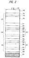
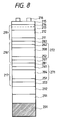
- Suitable for the photovoltaic element of the present invention include two types, for example, the single cell type shown in Fig. 1 or Fig. 5 and the stack cell type shown in Fig. 2 or Fig. 8.
- the structures of photovoltaic element and fabrication processes thereof according to the present invention will be explained in detail with reference to Fig. 1 and Fig. 2.
- Fig. 1 is an example of a schematic sectional view to show a single cell type photovoltaic element according to the present invention. It is noted that the present invention is by no means intended to be limited to the photovoltaic element in the structure of Fig. 1.
- reference numeral 101 designates a substrate, 102 a back electrode, 103 a first conduction type (n-type) semiconductor layer, 104 an i-type semiconductor layer, 105 a layer A forming a second conduction type (p-type) semiconductor layer, 106 a layer B also forming the second conduction type (p-type) semiconductor layer, 107 a transparent electrode, and 108 a collector electrode.
- Fig. 1 reference numeral 101 designates a substrate, 102 a back electrode, 103 a first conduction type (n-type) semiconductor layer, 104 an i-type semiconductor layer, 105 a layer A forming a second conduction type (p-type) semiconductor layer, 106 a layer B also forming the second conduction type (p-type) semiconductor layer, 107 a transparent electrode, and 108 a collector electrode.
- reference numeral 103 will be the first conduction type (p-type) semiconductor layer, 105 the layer A forming the second conduction type (n-type) semiconductor layer, and 106 the layer B forming the second conduction type (n-type) semiconductor layer.
- Fig. 1 shows the structure in which the light is made incident from the opposite side to the substrate, but, in the case of the photovoltaic element in the structure in which the light is incident from the substrate side, the element will be arranged in such a manner that the substrate 101 is transparent, the positions of the transparent electrode and the back electrode are switched, reference numeral 102 becomes the transparent electrode, 103 the first conduction type (p-type/n-type) semiconductor layer, 105 the layer A forming the second conduction type (n-type/p-type) semiconductor layer, 106 the layer B forming the second conduction type (n-type/p-type) semiconductor layer, and 107 the back electrode.
- Fig. 2 is an example of a schematic sectional view to show a stack cell type photovoltaic element according to the present invention. It is, however, noted that the present invention is by no means intended to be limited to the photovoltaic element in the structure of Fig. 2.
- the stack cell type photovoltaic element shown in Fig. 2 is of the laminate structure of three pin junctions, in which 219 is a first pin junction when counted from the light incidence side, 218 is a second pin junction, and 217 a third pin junction. These three pin junctions are stacked on a back electrode 202 formed on a substrate 201, and a transparent electrode 215 and a collector electrode 216 are formed on the top of the three pin junctions, thus forming the stack cell type photovoltaic element.
- Each of the pin junctions 217, 218, and 219 shown in Fig. 2 has a first conduction type (n-type/p-type) semiconductor layer 203, 207, or 211, an i-type semiconductor layer 271, 272, or 212, a layer A 205, 209, or 213 forming a second conduction type (p-type/n-type) semiconductor layer, and a layer B 206, 210, or 214 forming the second conduction type (p-type/n-type) semiconductor layer.
- Fig. 2 illustrates the example of the pin junctions 217 and 218 in each of which the i-layer 271 or 272 is composed of three regions.
- Each i-layer 271 or 272 has RF i-layers 251, 261 or 252, 262 formed utilizing the RF (radio frequency) band as discharge frequency and a ⁇ w i-layer 204 or 208 formed utilizing the microwave ( ⁇ wave) band as discharge frequency.
- the i-layer 271 or 272 may be formed as a single region, if desired characteristics are attained thereby.
- the locations of the doping layer and electrode will be switched depending upon the direction of incidence of light.
- Fig. 5 is a schematic sectional view to show a suitable example of structure of another photovoltaic element.
- portions denoted by the same reference numerals as those in Fig. 1 represent the same portions.
- the element shown in Fig. 5 is an example in which the substrate 101 also serves as a back electrode.
- Fig. 8 is a schematic sectional view to show an example of structure of still another preferred photovoltaic element.
- portions denoted by the same reference numerals as those in Fig. 2 represent the same portions.
- the element shown in Fig. 8 is formed in the same triple cell arrangement as the element shown in Fig. 2, but it is mainly different from the element shown in Fig. 2 in that only the cell closest to the light incidence side (the top cell) has the layer A and in that the semiconductor layers are formed through a buffer layer 292 after a reflective and conductive layer 291 is formed on the substrate 201.
- reference numerals 281 and 282 each denote second conduction type semiconductor layers.
- the substrate applied in the present invention can be properly selected with necessity, but it needs to be one at least permitting the semiconductor layers etc. to be formed thereon, as described above.
- crystal form of such a substrate for example, it may be either of single crystal or of non-single-crystal.
- Its electric property may be either conductive or insulating and may be properly selected depending upon the total structure of photovoltaic apparatus or upon procedures and steps of fabrication thereof.
- Its optical property may be either transparent or non-transparent.
- a preferably used substrate is one having less deformation or distortion but having desired strength.
- the material for the substrate include thin plates of metals such as Fe, Ni, Cr, Al, Mo, Au, Nb, Ta, V, Ti, Pt, or Pb or alloys such as brass or stainless steel, and composites thereof; films or sheets of heat-resistant synthetic resins such as polyester, polyethylene, polycarbonate, cellulose acetate, polypropylene, polyvinyl chloride, polyvinylidene chloride, polystyrene, polyamide, polyimide, or epoxy, or composites thereof with glass fibers, carbon fibers, boron fibers, or metal fibers; thin plates of the aforementioned metals or resin sheets of the aforementioned resins coated with a metal thin film of a different material and/or an insulating thin film such as SiO 2 , Si 3 N 4 , Al 2 O 3 , or AlN by sputtering, vapor deposition, plating, or the like; glass, ceramics, and so on.
- metals such as Fe, Ni, Cr, Al, Mo, Au, Nb
- the substrate When the substrate is a metal or the like being electrically conductive, it may be used also as an electrode for directly taking an electric current out. Further, if the substrate is a synthetic resin or the like being electrically insulative, the electrode for taking the electric current out is desirably formed by a preliminary surface treatment in a process of plating, vapor deposition, sputtering, or the like of a so-called metal itself or an alloy, such as Al, Ag, Pt, Au, Ni, Ti, Mo, W, Fe, V, Cr, Cu, stainless steel, brass, nichrome, SnO 2 , In 2 O 3 , ZnO, or ITO, and a transparent and conductive oxide (TCO) on the surface on which the deposit films are to be formed.
- a so-called metal itself or an alloy such as Al, Ag, Pt, Au, Ni, Ti, Mo, W, Fe, V, Cr, Cu, stainless steel, brass, nichrome, SnO 2 , In 2 O 3 , Zn
- the substrate is an electrically conductive one such as the metals or not
- a different metal layer or the like may be provided on the side where the deposit films are to be formed on the substrate for the purposes of improving the reflectivity of the light having passed through the semiconductor layers (for example, long-wavelength light) on the substrate surface, preventing mutual diffusion of constituent elements between the substrate material and the deposit films, and so on.
- the substrate is relatively transparent and the photovoltaic element is constructed in the layer structure in which the light is incident from the substrate side, it is desirable to preliminarily deposit the transparent and conductive oxide or a conductive thin film such as a metal thin film on the substrate.
- the surface of the substrate may be either a so-called smooth surface or a finely roughened surface.
- the roughness may be of a desired configuration including a sphere, a cone, a pyramid, or the like, but reflection of light on the surface becomes diffused reflection when the maximum height (Rmax) is preferably in the range of 0.05 ⁇ m to 2 ⁇ m. This can increase the optical pathlength of reflected light from the surface and can further improve the utilization factor of incident light.
- the configuration of the substrate may be a plate, an elongate belt (band), a cylinder, or the like with a smooth surface or a roughened surface depending upon applications, and the thickness thereof is properly determined so as to be capable of forming the photovoltaic element as desired. If the photovoltaic element is desired to be provided with flexibility or if the light is incident from the substrate side, the substrate may be formed as thin as possible within the range to sufficiently demonstrate the function as a substrate. However, the thickness of the substrate is normally 10 or more ⁇ m in view of fabrication of substrate, handling thereof, mechanical strength, and so on.
- a preferred material for the belt substrate suitably applicable is one having less deformation or distortion at temperatures necessary for fabrication of the semiconductor films, having desired strength, and having electrical conduction
- specific examples of the material include thin plates of metals such as stainless steel, aluminum and alloys thereof, iron and alloys thereof, or copper and alloys thereof, and composites thereof; the foregoing coated with a metal thin film of a different material and/or an electrically insulating thin film such as SiO 2 , Si 3 N 4 , Al 2 O 3 , or AlN by sputtering, vapor deposition, plating, or the like; sheets of heat-resistant resins such as polyimide, polyamide, polyethylene terephthalate, or epoxy or composites thereof with glass fibers, carbon fibers, boron fibers, or metal fibers the surface of which is treated to become electrically conductive by a method of plating, vapor deposition, sputtering, or coating of a metal alone or an alloy thereof, and
- a desired thickness of the belt substrate is as thin as possible within the range to demonstrate the strength enough to maintain a curved shape formed when carried by a carrying means in view of the cost, storage space, and so on.
- the thickness is preferably in the range of 0.01 mm to 5 mm, more preferably in the range of 0.02 mm to 2 mm, and most preferably in the range of 0.05 mm to 1 mm.
- the thickness can be determined to be relatively thin while maintaining the desired strength.
- a preferred width of the belt substrate is determined in the range to maintain uniformity of the plasma formed in each film-forming chamber and to suit module arrangement of photovoltaic element formed, and specifically, it is determined preferably in the range of 5 cm to 100 cm, and more preferably in the range of 10 cm to 80 cm.
- the length of the belt substrate may be of a length enough to be rolled up in a roll form or it may be formed in an elongated shape formed by welding or the like of elongate strips.
- a reflective and conductive film for improving the reflectivity on the substrate surface is formed on the substrate, as described above, specific examples of suitable materials for the reflective and conductive film include Ag, Al, Cr, Au, Cu, and so on.
- a transparent and conductive oxide film is preferably formed on the side of fabrication between the substrate and the semiconductor films.
- a suitable example of a material for the transparent and conductive oxide layer is ZnO.
- the back electrode in the present invention is an electrode disposed on the surface of the semiconductor layer opposite to the light incidence side.
- the back electrode is placed on the substrate, or at a position on the opposite side to the substrate through the semiconductor layers when the substrate is transparent and the light is incident from the substrate side.
- the material for the back electrode include metals such as gold, silver, copper, aluminum, nickel, iron, chromium, molybdenum, tungsten, titanium, cobalt, tantalum, niobium, zirconium, or the like or alloys such as stainless steel.
- metals with high reflectivity such as aluminum, copper, silver, or gold, are particularly preferred.
- the back electrode can also serve as a light reflecting layer for reflecting light not absorbed by the semiconductor layers back toward the semiconductor layers.
- the back electrode may be flat, but is more preferably roughened for scattering light.
- the back electrode When the back electrode is roughened for scattering the light, it scatters the long-wavelength light not absorbed by the semiconductor layers so as to extend the optical pathlength in the semiconductor layers, to enhance long-wavelength sensitivity of photovoltaic element and to increase the short-circuit current, whereby the photoelectric conversion efficiency can be increased. It is desired to determine the roughened configuration for scattering the light so that differences between peaks and bottoms of the roughened configuration drop in the range of Rmax being 0.05 ⁇ m to 2.0 ⁇ m, and more preferably in the range of 0.2 ⁇ m to 2.0 ⁇ m.
- the back electrode does not always have to be formed.
- the back electrode is formed using vapor deposition, sputtering, plating, printing, or the like. If the back electrode is formed in the roughened configuration for scattering the light, it is formed by subjecting a film of a metal or an alloy formed to dry etching, wet etching, sandblasting, heating, or the like.
- the roughened configuration for scattering the light can also be formed by vapor-depositing the aforementioned metal or alloy while heating the substrate.
- An anti-diffusion layer such as conductive zinc oxide may be further provided, though not shown, between the back electrode 102 and the first conduction type (n-type) semiconductor layer 103. Effects of the anti-diffusion layer are to prevent metal elements constituting the back electrode 102 from diffusing into the n-type semiconductor layer, to prevent short circuit from occurring at a defect such as a pinhole between the back electrode 102 and the transparent electrode 107 provided on either side of the semiconductor layers by provision of a little resistance, to cause multiple interference by a thin film to confine the light incident in the photovoltaic element, and so on.
- examples of semiconductor materials especially suitably used for the photovoltaic apparatus of the present invention include a-Si : H (hydrogenated amorphous silicon), a-Si : F (fluorinated amorphous silicon), a-Si : H : F (hydrogenated and fluorinated amorphous silicon), a-SiGe : H (hydrogenated amorphous silicon germanium), a-SiGe : F (fluorinated amorphous silicon germanium), a-SiGe : H : F (hydrogenated and fluorinated amorphous silicon germanium), a-SiC : H (hydrogenated amorphous silicon carbide), a-SiC : F (fluorinated amorphous silicon carbide), a-SiC : H : F (hydrogenated and fluorinated amorphous silicon carbide), or IV-group element based and IV-group alloy based non-sing
- the semiconductor layers can be modified by valence electron control and bandgap control. Specifically, it is realized by introducing a stock compound containing an element to become a valence electron controlling agent or a bandgap controlling agent into a film-forming space singly or in a mixture form with the stock gas for forming the deposit film or with the dilute gas, described previously, upon formation of semiconductor layer.
- the valence electron control makes at least some parts of the semiconductor layers doped in the first conduction type (the p-type or the n-type) and in the second conduction type (the n-type or the p-type opposite to the first conduction type), thereby forming at least one pin junction.
- the first conduction type the p-type or the n-type
- the second conduction type the n-type or the p-type opposite to the first conduction type
- Methods for forming the semiconductor layers may be selected from various CVD processes such as the microwave plasma CVD process, the RF plasma CVD process, the photo-assisted CVD process, the thermal CVD process, and the MOCVD process, various vapor deposition processes such as the EB vapor deposition, MBE, ion plating, and ion beam process, sputtering, spraying, printing, and so on.
- the plasma CVD process for decomposing the stock gas by plasma and depositing a film on the substrate is favorably used as a method industrially employed.
- a batch type apparatus or a continuous film-forming apparatus can be used as a reaction apparatus as occasion demands.
- the i-type layer used in the pin junction is an important layer for generating and transporting carriers with reception of irradiation light.
- the i-type layer may be a layer including a small p-type part or a small n-type part as long as it can function substantially as an i-type layer.
- the IV-group element based and IV-group alloy based non-single-crystal semiconductor materials may contain hydrogen atoms (H, D) or halogen atoms (X), as described above.
- the hydrogen atoms (H, D) or halogen atoms (X) contained in the i-type layer function to compensate for uncoupled bonds (dangling bonds) in the i-type layer and to improve a product of mobility and life of carriers in the i-type layer. They also function to compensate for the interface levels in each interface between the p-type layer and the i-type layer or between the n-type layer and the i-type layer, so as to present the effect to improve the photoelectromotive force, photocurrent, and optical response of the photovoltaic element.
- An optimum content of the hydrogen atoms or/and halogen atoms contained in the i-type layer is 1 to 40 atomic %. Especially, it is preferred that the hydrogen atoms or/and halogen atoms be distributed at higher contents on the side of each interface between the p-type layer and the i-type layer or between the n-type layer and the i-type layer.
- a preferably range of the contents of the hydrogen atoms or/and halogen atoms near the interfaces is 1.1 to 2 times greater than the content thereof in the bulk (at a position apart from the interfaces, for example, in a region near the center in the thickness direction). Further, a preferable arrangement is such that the content of the hydrogen atoms or/and halogen atoms changes according to the content of silicon atoms.
- a desired arrangement is such that a material for the i-type semiconductor layer in a pin junction close to the light incidence side is a material with a wide bandgap while a material for the i-type semiconductor layer in a pin junction apart from the light incidence side is a material with a narrow bandgap.
- An amorphous semiconductor material is preferably used as a material for the i-type semiconductor layer.
- amorphous silicon and amorphous silicon germanium are expressed with an element or elements for compensating for the dangling bonds, as a-Si : H, a-Si : F, a-Si : H : F, a-SiGe : H, a-SiGe : F, a-SiGe : H : F, or the like.
- Preferable characteristics of the i-type semiconductor layer suitably applicable for the photovoltaic element of the present invention are as follows: the content of hydrogen atoms (C H ) is 1.0 to 25.0 %; photoconductivity ( ⁇ p ) under irradiation with pseudo sunlight of AM 1.5 and 100 mW/cm 2 is 1.0 ⁇ 10 -7 or more S/cm; dark conductivity ( ⁇ d ) is 1.0 ⁇ 10 -9 or less S/cm; Urback energy by the constant photocurrent method (CPM) is 55 or less meV; localized level density is 10 or less /cm.
- C H hydrogen atoms
- ⁇ p photoconductivity
- ⁇ d dark conductivity
- Urback energy by the constant photocurrent method (CPM) is 55 or less meV
- localized level density is 10 or less /cm.
- the semiconductor layers By the valence electron control the semiconductor layers, at least some parts thereof, are doped in the first conduction type (the p-type or the n-type) and in the second conduction type (the n-type or the p-type opposite to the first conduction type), thereby forming at least one pin junction.
- the first conduction type the p-type or the n-type
- the second conduction type the n-type or the p-type opposite to the first conduction type
- the p-type semiconductor layer or the n-type semiconductor layer in the present invention is a layer for constituting the first conduction type semiconductor layer and the second conduction type semiconductor layer (layer A, layer B), characterizing the photovoltaic element of the present invention, and it is an important layer for influencing the characteristics thereof.
- a non-single-crystal material is suitably applicable for the material for the p-type semiconductor layer or the n-type semiconductor layer.
- the "non-single-crystal material" in the present invention means an amorphous material (expressed by a-), a microcrystalline material (expressed by ⁇ c-), and a polycrystalline material (expressed by poly-).
- the amorphous material or the microcrystalline material include materials obtained by adding a high concentration of a p-type valence electron controlling agent (the III-group atoms such as B, Al, Ga, In, and Tl in the Periodic Table) or an n-type valence electron controlling agent (the V-group atoms such as P, As, Sb, and Bi in the Periodic Table) to a-Si : H, a-Si : HX, a-SiC : H, a-SiC : HX, a-SiGe : H, a-SiGe : HX, a-SiGeC : H, a-SiGeC : HX, a-SiO : H, a-SiO : HX, a-SiN : H, a-SiN : HX, a-SiON : H, a-SiON : HX, a-Si
- polycrystal material examples include materials obtained by adding a high concentration of a p-type valence electron controlling agent (the III-group atoms such as B, Al, Ga, In, and Tl in the Periodic Table) or an n-type valence electron controlling agent (the V-group atoms such as P, As, Sb, and Bi in the Periodic Table) to poly-Si : H, poly-Si : HX, poly-SiC : H, poly-SiC : HX, poly-SiO : H, poly-SiO : HX, poly-SiN : H, poly-SiN : HX, poly-SiN : HX, poly-SiGeC : H, poly-SiGeC : HX, poly-SiON : H, poly-SiON : HX, poly-SiON : HX, poly-SiOCN : H, poly-SiOCN : H, poly-SiOC
- a crystalline semiconductor layer of less absorption of light or an amorphous semiconductor layer with a wide bandgap is suitable for the p-type layer or the n-type layer on the light incidence side.
- a desirable additive amount of the III-group atoms in the Periodic Table into the p-type layer and a desired additive amount of the V-group atoms in the Periodic Table into the n-type layer are 0.1 to 50 atomic %.
- the hydrogen atoms (H, D) or halogen atoms contained in the p-type layer or in the n-type layer function to compensate for the uncoupled bonds in the p-type layer or in the n-type layer to increase the doping efficiency of the p-type layer or the n-type layer.
- the hydrogen atoms or halogen atoms are added preferably in the range of 0.1 to 40 atomic % into the p-type layer or into the n-type layer.
- the hydrogen atoms or the halogen atoms are added preferably in the range of 0.1 to 8 atomic %.
- a preferred distribution form is a distribution of contents in which the hydrogen atoms or/and halogen atoms are distributed more on the side of each interface between the p-type layer and the i-type layer or between the n-type layer and the i-type layer, and a preferable range of the contents of the hydrogen atoms or/and halogen atoms near the interfaces is a range 1.1 to 2 times greater than the contents in the bulk.
- Defect level density or mechanical distortion near the interfaces can be decreased by the arrangement in which the content of the hydrogen atoms or halogen atoms is increased near each interface between the p-type layer and the i-type layer or between the n-type layer and the i-type layer, whereby the photoelectromotive force and photocurrent of photovoltaic element of the present invention can be increased.
- the activation energy is preferably 0.2 or less eV and more preferably 0.1 or less eV.
- the resistivity is preferably 100 or less ⁇ cm and more preferably 1 or less ⁇ cm.
- the film thickness of the p-type layer and the n-type layer is preferably in the range of 1 to 50 nm and more preferably in the range of 3 to 10 nm.
- fabrication processes suitable for forming the IV-group element based and IV-group alloy based amorphous semiconductor layers suitable for the semiconductor layers in the photovoltaic apparatus of the present invention include the plasma CVD processes using an alternating current or high frequency waves, such as the RF plasma CVD process or the microwave plasma CVD process.
- the microwave plasma CVD process is a method for forming a desired deposit film on a substrate placed in a deposition chamber, in which a material gas including a stock gas, a dilute gas, etc. is introduced into the deposition chamber (vacuum chamber), which can be set into a reduced-pressure state, the internal pressure in the deposition chamber is set at a desired pressure as evacuating the inside by a vacuum exhaust pump, microwaves oscillated by a microwave power supply are guided through a waveguide tube and through a dielectric window (alumina ceramics or the like) into the deposition chamber, and the material gas is decomposed to produce plasma thereof, thereby forming a desired deposit film on the substrate set in the deposition chamber.
- the microwave plasma CVD process can form deposit films applicable for the photovoltaic apparatus, under wide deposition conditions.
- the substrate temperature in the deposition chamber is between 100 and 450 °C; the internal pressure is between 0.5 and 30 mTorr; the microwave power is between 0.01 and 1 W/cm 3 ; the frequency of microwave is between 0.1 and 10 GHz.
- the substrate temperature in the deposition chamber is between 100 and 350 °C; the internal pressure is between 0.1 and 10 Torr; the RF power is between 0.001 and 5.0 W/cm 3 ; the deposition rate is between 0.01 and 3 nm/sec.
- stock gas suitable for deposition of the IV-group element based and IV-group alloy based amorphous semiconductor layers suitable for the photovoltaic apparatus of the present invention include gasifiable compounds containing the silicon atom, gasifiable compounds containing the germanium atom, gasifiable compounds containing the carbon atom, and mixture gases of the foregoing compounds.
- gasifiable compounds containing the silicon atom include chain or cyclic silane compounds, and more specifically, gas states or readily gasifiable states of SiH 4 , Si 2 H 6 , SiF 4 , SiFH 3 , SiF 2 H 2 , SiF 3 H, Si 3 H 8 , SiD 4 , SiHD 3 , SiH 2 D 2 , SiH 3 D, SiFD 3 , SiF 2 D 2 , Si 2 D 3 H 3 , (SiF 2 ) 5 , (SiF 2 ) 6 , (SiF 2 ) 4 , Si 2 F 6 , Si 3 F 8 , Si 2 H 2 F 4 , Si 2 H 3 F 3 , SiCl 4 , (SiCl 2 ) 5 , SiBr 4 , (SiBr 2 ) 5 , Si 2 Cl 6 , SiHCl 3 , SiH 2 Br 2 , SiH 2 Cl 2 , Si 2 Cl 3 F 3 , and so on.
- gasifiable compounds containing the germanium atom include GeH 4 , GeD 4 , GeF 4 , GeFH 3 , GeF 2 H 2 , GeF 3 H, GeHD 3 , GeH 2 D 2 , GeH 3 D, Ge 2 H 6 , Ge 2 D 6 , and so on.
- Examples of elements for expanding the bandgap of the i-type semiconductor layer used in forming the first p-type semiconductor layer in the photovoltaic element of the present invention include carbon, oxygen, nitrogen, and so on.
- Specific examples of the gasifiable compounds containing the carbon atom include CH 4 , CD 4 , C n H 2n+2 (n is an integer), C n H 2n (n is an integer), C 2 H 2 , C 6 H 6 , CO 2 , CO, and so on.
- gases containing nitrogen include N 2 , NH 3 , ND 3 , NO, NO 2 , N 2 O, and so on.
- gases containing oxygen include O 2 , CO, CO 2 , NO, NO 2 , N 2 O, CH 3 CH 2 OH, CH 3 OH, and so on.
- Examples of the substance introduced for valence electron control into the p-type layer or into the n-type layer are the III-group atoms and the V-group atoms in the Periodic Table.
- starting materials effectively used for introducing the III-group atoms are as follows.
- Specific examples of the starting materials for introducing boron atoms include boron hydrides such as B 2 H 6 , B 4 H 10 , B 5 H 9 , B 5 H 11 , B 6 H 10 , B 6 H 12 or B 6 H 14 and boron halides such as BF 3 or BCl 3 .
- further starting materials applicable include AlCl 3 , GaCl 3 , InCl 3 , TlCl 3 , and so on.
- B 2 H 6 and BF 3 are suitable.
- Examples of starting materials effectively used for introducing the V-group atoms are as follows.
- Specific examples of the starting materials for introducing phosphorus atoms include phosphorus hydrides such as PH 3 or P 2 H 4 and phosphorus halides such as PH 4 I, PF 3 , PH 5 , PCl 3 , PCl 5 , PBr 3 , PBr 5 , or PI 3 .
- further materials applicable include AsH 3 , AsF 3 , AsCl 3 , AsBr 3 , AsF 5 , SbH 3 , SbF 3 , SbF 5 , SbCl 3 , SbCl 5 , BiH 3 , BiCl 3 , and BiBr 3 .
- PH 3 and PF 3 are suitable.
- the gasifiable compound may be introduced into the deposition chamber as properly diluted with a gas of H 2 , He, Ne, Ar, Xe, Kr, or the like, or a gas selected from these may be separately introduced into the deposition chamber.
- preferred conditions are such that the stock gas is diluted at a dilution ratio of 2 to 100 with hydrogen gas and that the microwave power, or relatively high power as the RF power is applied.
- the layer A constituting the second conduction type (p-type or n-type) semiconductor layer is formed in such a manner that, after formation of the i-type semiconductor layer, the surface of the i-type semiconductor layer is exposed to plasma containing the p-type or n-type valence electron controlling agent whereby the i-type semiconductor layer near the surface is converted into the p-type or n-type region, or that the bandgap is further expanded.
- the plasma containing the p-type or n-type valence electron controlling agent means glow discharge plasma produced by application of DC, AC, or high frequency wave.
- the frequency applicable may be selected from various frequencies ranging DC to microwaves of approximately 10 GHz.
- the material gas for forming the plasma is selected from stock gases suitable for deposition of the IV-group element based and IV-group alloy based amorphous semiconductor layers as described previously, gases containing substances suitable for the valence electron control as described previously, and mixtures thereof with the dilute gas as described previously.
- the stock gases suitable for deposition of the IV-group element based and IV-group alloy based amorphous semiconductor layers stated above do not always have to be used.
- the forming conditions are selected so as to mainly cause the reaction for converting the i-type semiconductor layer near the surface into the p-type or n-type region or further to mainly cause injection of the element for expanding the bandgap of the i-type semiconductor layer, rather than the deposition reaction.
- the p-type or n-type valence electron controlling agent and the element for expanding the bandgap of the i-type semiconductor layer are injected from the surface of the i-type semiconductor layer into a very shallow region, thereby converting the i-type semiconductor layer near the surface into the p-type or n-type region.
- the depth of the p-type or n-type region differs depending upon the conditions of plasma, but it is desirably between 1.0 nm and 10 nm.
- This injection of the valence electron controlling agent and the element for expanding the bandgap of the i-type semiconductor layer into the i-type semiconductor layer by glow discharge plasma is utterly different from the conventional ion implantation used in crystal silicon or the like.
- ions are accelerated in a beam form and the energy of ions is high; whereas, in the injection by glow discharge plasma energy of the substances injected is low and they are injected from the surface of the i-type semiconductor layer only into a very shallow region. Fine control of depth of injection is also easy and uniform injection is readily effected across a large area.
- the doping layer with less local levels can be formed without deteriorating film quality of the i-type semiconductor layer. Accordingly, the layer A constituting the second conduction type (p-type or n-type) semiconductor layer can be formed uniformly across a large area and with good film quality.
- the pressure of gas low can raise the injection efficiency of the valence electron controlling agent or the element for expanding the bandgap of the i-type semiconductor layer.
- the details of this mechanism are not clarified yet, but it is conceivably because the self bias of electrode becomes higher with a decrease of the pressure of gas, which increases the energy of positive ions decomposed in the plasma state. Another possible cause is an increase in mean free path of positive ions.
- the valence electron controlling agent can be restricted from depositing on the surface of the i-type semiconductor layer, which can avoid the negative effect, such as an increase of light absorption coefficient, due to deposition of the valence electron controlling agent.
- a preferred range of the gas pressure differs depending upon a type of the mixture gas, the frequency of power applied to the plasma, or input power, but, for example in the case of use of the RF CVD process, it is desirably between 0.01 and 1 Torr.
- a preferred range of the DC voltage or AC power differs depending upon a type of the mixture gas, the frequency of the power applied to the plasma, or the gas pressure, but, for example in the case of use of the RF CVD process, desired power is 0.01 or more W/cm 3 .
- the plasma produces ions or radicals of hydrogen, which have etching effect, and therefore, even if the mixture gas contains a stock gas suitable for deposition of the aforementioned IV-group element based and IV-group alloy based amorphous semiconductor layers, an increase of the dilution ratio with hydrogen gas can control deposition of the stock gas, thus well injecting the valence electron controlling agent or the element for expanding the bandgap of the i-type semiconductor layer. It can also restrict the valence electron controlling agent from depositing on the surface of the i-type semiconductor layer.
- hydrogen atoms as well as the valence electron controlling agent, are injected into the region near the surface of the i-type semiconductor layer, which work to compensate for uncoupled bonds (dangling bonds) in the i-type semiconductor layer, occurring due to injection of the valence electron controlling agent, and which can enhance an activation rate of acceptors or donors.
- the bandgap of the i-type semiconductor layer is further expanded near the surface, light absorption is decreased in the first p-type semiconductor layer or n-type semiconductor layer to increase the short-circuit current (J sc ) of photovoltaic element, and the built-in potential is increased so as to raise the open-circuit voltage (V oc ), whereby the photoelectric conversion efficiency can be improved.
- a preferred range of the dilution ratio with hydrogen gas differs depending upon a type of the mixture gas, the frequency of power applied to the plasma, the power, or the gas pressure, but, for example in the case of use of the RF CVD process, a desired flow rate of hydrogen is 100 or more where 1 is taken as a flow rate of a sum of the stock gas suitable for deposition of the IV-group element based and IV-group alloy based amorphous semiconductor layers and the stock gas of the valence electron controlling agent.
- the layer B constituting the second conduction type (p-type or n-type) semiconductor layer is desirably to be more heavily doped than the ordinary doping layers are and to have a smaller film thickness.
- a preferable range of the film thickness of the layer B constituting the second conduction type (p-type or n-type) semiconductor layer is between 1 nm and 10 nm.
- the frequency of the power used in forming the layer A is preferably set lower than the frequency of the power used in forming the layer B.
- the frequency upon forming the layer A is desirably selected from the range of 5 to 500 kHz while the frequency upon forming the layer B is desirably selected from the range of 1 to 100 MHz.
- Preferred discharge power this time is between 0.01 and 5 W/cm 2 for the layer A and between 0.0001 and 1 W/cm 2 for the layer B.
- the first p-type (n-type) semiconductor layer (which is the layer A constituting the second conduction type semiconductor layer) is formed by plasma doping using the discharge power of a lower frequency than the frequency of the high-frequency power used in the step for forming the second p-type (n-type) semiconductor layer (which is the layer B constituting the second conduction type semiconductor layer), whereby impurity ions are first injected with efficiency into the surface of the i-type semiconductor layer, thereby forming the first p-type (n-type) semiconductor layer containing crystalline substance.
- the second p-type (n-type) semiconductor layer consisting of only amorphous substance is formed on the first p-type (n-type) semiconductor layer by the RF plasma CVD process, whereby the stacked semiconductor films for the photovoltaic element with a high photoelectric conversion efficiency can be formed across a large area and without dispersion or unevenness of characteristics.
- the impurity ions are first injected into the surface of the i-type semiconductor layer and the outermost surface of the layer A is greatly damaged.
- the surface levels become interface levels between the transparent electrode and the p-type (or n-type) semiconductor layer, which increases the activation energy at the outermost surface of the p-type (or n-type) semiconductor layer or which distorts the internal potential in the photovoltaic element as trapping the carriers.
- the surface levels negatively affect movement of carriers between the transparent electrode and the p-type (or n-type) semiconductor layer.
- the amorphous semiconductor can uniformly cover the surface levels existing in the outermost surface of the layer A greatly damaged, when the layer B consisting of only the amorphous substance is formed on the layer A by the RF plasma CVD process, which can decrease the surface levels.
- the surface levels are prevented from negatively affecting the movement of carriers between the transparent electrode and the p-type (or n-type) semiconductor layer, whereby the stacked semiconductor layers for photovoltaic element with high photoelectric conversion efficiency can be formed across a large area and without dispersion or unevenness of characteristics, presumably.
- the transparent electrode 107 in the present invention serves as an electrode on the light incidence side to transmit the light and also serves as an anti-reflection film in the optimum thickness.
- Requirements for the transparent electrode 107 are high transmittance in the wavelength region which the semiconductor layers can absorb, and low resistivity.
- the transmittance at 550 nm is 80 or more % and more preferably 85 or more %.
- the resistivity is preferably 5 ⁇ 10 -3 or less ⁇ cm and more preferably 1 ⁇ 10 -3 or less ⁇ cm.
- Examples of materials preferably applicable for the transparent electrode include conductive oxides, such as In 2 O 3 , SnO 2 , ITO (In 2 O 3 + SnO 2 ), ZnO, CdO, Cd 2 SnO 4 , TiO 2 , Ta 2 O 5 , Bi 2 O 3 , MoO 3 , or Na x WO 3 , or mixtures thereof.
- An element (dopant) for changing the electric conductivity may be added to these compounds.
- the element (dopant) for changing the electric conductivity examples include Al, In, B, Ga, Si, and F; in the case of In 2 O 3 , they include Sn, F, Te, Ti, Sb, and Pb; and in the case of SnO 2 , they include F, Sb, P, As, In, Tl, Te, W, Cl, Br, and I.
- a method for forming the transparent electrode 107 suitably applicable is the vapor deposition process, the CVD process, the spraying process, the spin-on process, the dipping process, or the like.
- the collector electrode 108 in the present invention is formed on a part of the transparent electrode 107 with necessity, where the resistivity of the transparent electrode 107 is not sufficiently low. It works to decrease the resistivity of the electrode so as to lower series resistance of photovoltaic element.
- a material for the collector electrode include metals such as gold, silver, copper, aluminum, nickel, iron, chromium, molybdenum, tungsten, titanium, cobalt, tantalum, niobium, or zirconium, alloys such as stainless steel, and conductive pastes using a powdered metal. It is formed in a branched pattern so as not to interrupt the incident light into the semiconductor layer.
- Fig. 3 is a schematic plan view of the photovoltaic element, observed from the light incidence side. As shown in Fig. 3, the branched configuration of the collector electrode 108 can decrease the substantial resistance with efficiency and without impeding the incident light from entering the element.
- a more reduction of substantial resistance can be expected by increasing the width of strips horizontally extending in the branched pattern.
- output efficiency can be further improved by increasing the widths of the strips as the distance to the output decreases.
- an area occupied by the collector electrode is preferably 15 or less %, more preferably 10 or less %, and most preferably 5 or less %.
- a mask is used for forming the pattern of the collector electrode, and a method for forming it may be the vapor deposition process, the sputtering process, the plating process, the printing process, or the like.
- the photovoltaic elements of the present invention are connected in series or in parallel, protection layers are formed on the top and bottom surfaces, and take-out electrodes of output etc. are attached.
- a diode for preventing a reverse current is sometimes incorporated.
- Examples of the fabricating apparatus of the photovoltaic element according to the present invention include the continuous forming apparatus of stacked semiconductor films as shown in Fig. 4 or Fig. 6.
- the apparatus of Fig. 4 is used when the form of the substrate is a plate (single plate type), while the apparatus of Fig. 6 is used when the form of the substrate is a belt (continuous type).
- reference numeral 401 designates a load lock chamber (input room), 402 a carrying room (chamber) for the n-type layer (or the p-type layer), 403 a carrying room (chamber) for the i-layer, 404 a carrying room (chamber) for the p-type layer (or the n-type layer), and 405 an unload chamber (take-out room).
- Numerals 406, 407, 408, and 409 each denote gate valves, which are provided for communication between adjacent rooms or for establishing independence of each room.
- Numerals 410, 411, and 412 each denote heaters for heating the substrate, and numeral 413 denotes substrate carrying rails as a substrate carrying means.
- Numeral 417 represents a deposition chamber for formation of the n-type layer (or the p-type layer), 418 a deposition chamber for formation of the i-layer, and 419 a deposition chamber for formation of the p-type layer (or the n-type layer).
- Each deposition chamber 417, 419 has an RF introducing cup 420 or 421 connected to an RF power supply 422 or 423, inside thereof.
- a gas supply pipe 429, 449, 469 is connected to each deposition chamber, whereby a desired gas can be supplied into each deposition chamber.
- a microwave introducing pipe 426 is connected through a microwave introducing window 425 to the deposition chamber 418, so that microwaves generated by a microwave generating means not shown can be guided through the microwave introducing pipe 426 and the microwave introducing window 425 into the deposition space.
- Numeral 424 designates a bias applying power supply for generating a bias voltage applied to the deposition chamber (or to the substrate in the chamber).
- An enlarged view of the deposition chamber for forming the i-layer is shown in a circle in the drawing, and, as shown inside the circle, the bias power supply is electrically connected to a bias electrode set inside the deposition space.
- Numeral 427 is a shutter, which is opened or closed with necessity.
- the heating heaters 410, 411, and 412 are movable in the directions of arrows. Each heater is moved with necessity from the side of carrying rails 413 to the deposition chamber 417, 418, 419 together with the substrate 490, and the substrate 490 can be moved from the side of the deposition chamber 417, 418, 419 to the carrying rails 413.
- an exhaust means such as a vacuum pump, not shown, is connected through a conductance valve not shown to each chamber.
- Fig. 6 is a schematic explanatory drawing to show a basic example of the continuous forming apparatus for continuously forming the stacked semiconductor films according to the present invention.
- the continuous forming apparatus of stacked semiconductor films according to the present invention is basically composed of a feeding chamber 601 of belt substrate, a film-forming chamber 602 for forming the n-type semiconductor layer (i.e., the first conduction type semiconductor layer) by the RF plasma CVD process, an i-type semiconductor layer forming chamber 603 for forming the i-type semiconductor layer by the RF plasma CVD process, a film-forming chamber 604 for forming the first p-type semiconductor layer (i.e., the layer A constituting the second conduction type semiconductor layer) by plasma doping, a film-forming chamber 611 for forming the second p-type semiconductor layer (i.e., the layer B constituting the second conduction type semiconductor layer) by the RF plasma CVD process, and a winding chamber 605 for winding up the belt substrate.
- the belt substrate 607 is fed out from a bobbin 608 in the feeding chamber 601 of belt substrate and is carried through the four film-forming chambers connected by the gas gates before rolled up on a bobbin 609 in the belt substrate winding chamber 605. While the substrate is carried through the four film-forming chambers, the stacked films of non-single-crystal semiconductors are formed in the nip structure on the surface thereof.
- Fig. 7 is a schematic sectional view for explaining an example of the film-forming chambers in the apparatus shown in Fig. 6.
- reference numeral 701 designates a belt substrate, 702 a vacuum container, 703, 704 gas gates, 705 a discharge chamber, 706 a discharge electrode, 707 a stock gas introducing pipe, 708 an exhaust pipe, 709 a block heater, 710 a discharge chamber-to-outside exhaust port, 711 a forming region aperture adjusting plate, 712 a film-forming chamber lid, 713, 714 heaters, 715, 716 thermocouples, 717 a reflector, 718 support rollers, 719 a separation passage, and 720 a gate gas introducing pipe.
- the belt substrate 701 is guided into or out of the film-forming space through the gas gate 703 or 704.
- a gas giving no negative effect on the film formation such as He gas or H 2 gas
- the pressure inside the vacuum container 702 can be decreased by the exhaust means such as a vacuum pump through the exhaust pipe 708.
- the exhaust means such as a vacuum pump through the exhaust pipe 708.
- the belt substrate 701, supplied through the separation passage 719, is carried into the film-forming space while the position thereof is regulated by the support rollers 718.
- the substrate 701 can be heated at a desired temperature by the heaters 713, 714 utilizing lamp heaters such as halogen lamps.
- the reflector 717 is provided on the opposite side of the heaters 713, 714 to the substrate 701, so that heat from the heaters 713, 714 such as lamp heaters can be reflected toward the substrate with efficiency.
- the discharge electrode 706 is disposed as facing to the film-forming surface of the substrate 701, and the block heater 709 is disposed on the opposite side of the discharge electrode 706 to the substrate 701.
- the stock gas is supplied through the stock gas introducing pipe 707 to the back face of the block heater 709 and is emitted from here into the film-forming space.
- the substrate 701 having passed through the film-forming space, is carried through the gas gate 704 as supported by the supporting rollers 718 in the same manner as when entering the film-forming space.
- Fig. 9 is a schematic, sectional, structural drawing to explain an example of the film-forming apparatus having a triple cell structure.
- reference numeral 901 designates a feeding chamber for the belt substrate, A a film-forming chamber set for forming a bottom cell in the lowest part, B a film-forming chamber set for forming a middle cell in a middle part, C a film-forming chamber set for forming a top cell in the outermost part, 902A, 902B, 902C film-forming chambers each for forming the first conduction type semiconductor layer utilizing the RF plasma, 903A, 903B, 903C, 911A, 911B film-forming chambers for forming the i-type semiconductor layer utilizing the RF plasma, 910A, 910B film-forming chambers for forming the i-type semiconductor layer utilizing the microwave plasma, 904A, 904B, 911C film-forming chambers for forming the second conduction type semiconductor layer utilizing the RF plasma, 904C a film-forming chamber for forming the second conduction type semiconductor layer (the layer A) by plasma doping, 905 a winding chamber for the belt
- the belt substrate 907 is fed out from the feeding bobbin 908, is carried through the gas gates 906 and the respective film-forming rooms (chambers) continuously arranged as the films are formed thereon, and is again wound up on the winding bobbin on the opposite side.
- Fig. 9 shows the arrangement of film-forming chambers along the arcuate configuration of the belt substrate 907, which is employed because deflection of the substrate 907 due to its own weight is taken into account in order to carry the substrate more smoothly.
- Fig. 10 is a schematic sectional view for explaining a suitable example of the film-forming chamber utilizing the microwave, applicable to the film-forming chambers shown in Fig. 9 (or Fig. 6).
- portions denoted by the same reference numerals as those shown in Fig. 7 represent the same members.
- Numeral 1002 represents a discharge chamber unit, 1009 a conductance valve, 1010 an exhaust pipe for primary evacuation, 1014 a bias electrode, 1021 a microwave introducing window, 1022 a perforated partition plate, 1023 a pressure measuring pipe, 1024 a forming chamber temperature adjuster, and 1025 a substrate temperature adjuster (a heater or the like).
- the photovoltaic element having the non-single-crystal silicon based semiconductor material will be explained in detail, but it is noted that the present invention is by no means limited by the description in the following.
- Examples 1 to 10 were carried out to investigate the cases where the second conduction type semiconductor layer had the layer A formed by exposing the surface of the i-type semiconductor layer to the plasma containing the valence electron controlling agent and the layer B deposited on the layer A by the CVD process using at least the valence electron controlling agent and the main constituent element of the i-type semiconductor layer.
- Examples 11 to 20 were carried out to investigate the cases where the layer A further contained the element for expanding the bandgap.
- Examples 21 to 28 were carried out to investigate the cases where the layer B further contained the element for expanding the bandgap.
- Examples 29 to 38 were carried out to investigate the cases where the layer A and the layer B each further contained the element for expanding the bandgap.
- Examples 39 to 41 were carried out to investigate the discharge power and the frequency thereof used in forming the layer A and the layer B.
- the single cell type photovoltaic element shown in Fig. 1 was fabricated using the deposition apparatus of Fig. 4.
- the p-type semiconductor layer being the second conduction type semiconductor layer, was comprised of the layer A formed by exposing the surface of the i-type semiconductor layer to the plasma containing the p-type valence electron controlling agent and the layer B formed on the surface of the layer A by depositing the p-type valence electron controlling agent and the main constituent element of the i-type semiconductor layer thereon.
- Example 2 This example is different from Example 1 in that the first p-type semiconductor layer or p1 layer (layer A) was not formed. Further, the film thickness of the second p-type semiconductor layer or p2 layer (layer B) of a-Si was 8 nm.
- the photovoltaic element fabricated in this example will be called as SC Comp Ex 1-1.
- Example 2 This example is different from Example 1 in that the following conditions were employed instead of those in Example 1 in forming the second p-type semiconductor layer or p2 layer (layer B).
- the photovoltaic element fabricated in this example will be called as SC Ex 2.
- Example 2 This example is different from Example 2 in that the first p-type semiconductor layer or p1 layer (layer A) was not formed.
- the film thickness of the second p-type semiconductor layer or p2 layer (layer B) of ⁇ c-Si was 8 nm.
- the photovoltaic element fabricated in this example will be called as SC Comp Ex 2-1.
- This example is different from Example 2 in that a-SiGe was used as a material for forming an MW i-type layer (an i-type semiconductor layer formed by the microwave CVD process) instead of a-Si.
- the photovoltaic element fabricated in this example will be called as SC Ex 3.
- Example 3 This example is different from Example 3 in that the first p-type semiconductor layer or p1 layer (layer A) was not formed.
- the film thickness of the second p-type semiconductor layer or p2 layer (layer B) of ⁇ c-Si was 8 nm.
- the photovoltaic element fabricated in this example will be called as SC Comp Ex 3-1.
- This example is different from Example 2 in that a-SiC was used as a material for forming an MW i-type layer (an i-type semiconductor layer formed by the microwave CVD process) instead of a-Si.
- the photovoltaic element fabricated in this example will be called as SC Ex 4.
- Example 4 This example is different from Example 4 in that the first p-type semiconductor layer or p1 layer (layer A) was not formed.
- the film thickness of the second p-type semiconductor layer or p2 layer (layer B) of ⁇ c-Si was 8 nm.
- the photovoltaic element fabricated in this example will be called as SC Comp Ex 4-1.
- Example 2 had the p layer on the light incidence side in the layer structure of substrate / n layer / i layer / p1 layer (layer A) / p2 layer (layer B) whereas this example had the n layer on the light incidence side in the layer structure of substrate / p layer / i layer / n1 layer (layer A) / n2 layer (layer B).
- the photovoltaic element fabricated in this example will be called as SC Ex 5.
- Example 5 This example is different from Example 5 in that the first n-type semiconductor layer or n1 layer (layer A) was not formed. Further, the film thickness of the second n-type semiconductor layer or n2 layer (layer B) of ⁇ c-Si was 8 nm.
- the photovoltaic element fabricated in this example will be called as SC Comp Ex 5-1.
- Table 9 shows results of the photoelectric conversion efficiency ( ⁇ ), open-circuit voltage (V oc ), short-circuit current (J sc ), and fill factor (F. F.) measured for such samples. Each value in the table indicates a numerical value normalized with a corresponding measured value of (SC Comp Ex 5-1) being 1.0. TABLE 9 P-E conversion efficiency ( ⁇ ) Open-ckt volt (Voc) Short-ckt current (Jsc) Fill factor (F. F) (SC Ex 5) 1.09 1.03 1.01 1.05
- Example 1 produced the photovoltaic element of the single cell type shown in Fig. 1 whereas this example produced a photovoltaic element of the triple cell type (the stack cell type of the structure in which three pin-type semiconductor junctions are stacked) shown in Fig. 2.
- the deposition apparatus used was such a modification of the apparatus of Fig. 4 that the number of deposition chambers as shown in Fig. 4 was increased as they were connected through plural gate valves.
- the layer structure of the photovoltaic element of this example was of substrate 201 / back electrode 202 / first pin junction / second pin junction / third pin junction / transparent electrode 215 / collector electrode 216.
- Each pin junction was of the following layer structure from the substrate side.
- the first pin junction 217 has the layer structure of, in order from the side of the back electrode 202, RF n-type layer (n1 layer) 203 of a-Si / RF i-type layer 251 of a-Si / MW i-type layer (i1 layer) 204 of a-SiGe / RF i-type layer 261 of a-Si / first p-type semiconductor layer (p11 layer, or the layer A) 205 formed by exposing the surface of the i-type semiconductor layer (RF i-type layer) 261 to the plasma containing the p-type valence electron controlling agent / second p-type semiconductor layer (p12 layer, or the layer B) 206 formed by depositing the p-type valence electron controlling agent and main constituent element of the i-type semiconductor layer.
- the second pin junction 218 has the layer structure of, in order from the side of the first pin junction 217, RF n-type layer (n2 layer) 207 of a-Si / RF i-type layer 252 of a-Si / MW i-type layer (i2 layer) 208 of a-SiGe / RF i-type layer 262 of a-Si / first p-type semiconductor layer (p21 layer, or the layer A) 209 formed by exposing the surface of the i-type semiconductor layer (RF i-type layer 262) to the plasma containing the p-type valence electron controlling agent / second p-type semiconductor layer (p22 layer, or the layer B) 210 formed by depositing the p-type valence electron controlling agent.
- the third pin junction 219 has the layer structure of, in order from the side of the second pin junction 218, RF n-type layer (n3 layer) 211 of a-Si / RF i-type layer (i3 layer) 212 of a-Si / first p-type semiconductor layer (p31 layer, or the layer A) 213 formed by exposing the surface of the i-type semiconductor layer (i3 layer 212) to the plasma containing the p-type valence electron controlling agent / second p-type semiconductor layer (p32 layer, or the layer B) 214 formed by depositing the p-type valence electron controlling agent.
- a process for fabricating the photovoltaic element of this example will be explained according to its procedures.
- Numerals in parentheses represent steps, wherein (1) and (2) are preparation steps, (3) - (6) forming steps for forming the first pin junction 217, (7) - (10) forming steps for forming the second pin junction 218, and (11) - (14) forming steps for forming the third pin junction 219.
- ITO was deposited as a transparent and conductive layer 215 in the thickness of 70 nm on the RF p-type layer 214 by the vacuum vapor deposition process.
- a mask with a comb-shaped aperture was mounted on the transparent and conductive layer 212, and the comb-shaped collector electrode 216 was deposited in the structure of Cr (400 nm)/Ag (1000 nm)/Cr (40 nm) in this order by the vacuum vapor deposition process.
- the photovoltaic element fabricated in this example will be called as SC Ex 6.
- Example 6 This example is different from Example 6 in that the first p-type semiconductor layers (p11 layer, p21 layer, p31 layer, or the layers A) were not formed. Further, the film thickness of the second p-type semiconductor layers (p12 layer, p22 layer, p32 layer, or the layers B) of ⁇ c-Si was 8 nm.
- the photovoltaic element fabricated in this example will be called as SC Comp Ex 6-1.
- Example 6 formed the photovoltaic element of the triple cell type with the p layers on the light incidence side whereas this example formed a photovoltaic element of the triple cell type with the n layers on the light incidence side, similar to Example 5.
- the photovoltaic element fabricated in this example will be called as SC Ex 7.
- Example 7 This example is different from Example 7 in that the first n-type semiconductor layers (n11 layer, n21 layer, n31 layer, or the layers A) were not formed. Further, the film thickness of the second n-type semiconductor layers (n12 layer, n22 layer, n32 layer, or the layers B) of ⁇ c-Si was 8 nm.
- the photovoltaic element fabricated in this example will be called as SC Comp Ex 7-1.
- Example 6 This example is different from Example 6 in that the following conditions were employed instead of those in Example 6 in forming the first p-type semiconductor layers (P11 layer, p21 layer, p31 layer, or the layers A).
- the photovoltaic element fabricated in this example will be called as SC Ex 8.
- This solar cell was evaluated by SIMS, which showed that the first p-type semiconductor layer had a hydrogen content larger than that of the i-type semiconductor layer.
- Example 2 This example is different from Example 2 in that the following conditions were employed instead of those in Example 2 in forming the first p-type semiconductor layer (p1 layer, or the layer A) 105 and the second p-type semiconductor layer (p2 layer, or the layer B) 106.
- the photovoltaic element fabricated in this example will be called as SC Ex 9.
- Example 2 This example is different from Example 2 in that the following conditions were employed instead of those in Example 2 in forming the first p-type semiconductor layer (p1 layer, or the layer A) 105 and the second p-type semiconductor layer (p2 layer, or the layer B) 106.
- the photovoltaic element fabricated in this example will be called as SC Ex 10.
- This example is different from Example 1 in that the layer A was formed by exposing the surface of the i-type semiconductor layer to the plasma containing the p-type valence electron controlling agent and the element for expanding the bandgap of the i-type semiconductor layer.
- the single cell type photovoltaic element shown in Fig. 1 was fabricated using the deposition apparatus of Fig. 4.
- the p-type semiconductor layer being the second conduction type semiconductor layer, was comprised of the layer A formed by exposing the surface of the i-type semiconductor layer to the plasma containing the p-type valence electron controlling agent and the element for expanding the bandgap of the i-type semiconductor layer, and the layer B formed on the surface of the layer A by depositing the p-type valence electron controlling agent and the main constituent element of the i-type semiconductor layer thereon.
- Example 11 This example is different from Example 11 in that the first p-type semiconductor layer or p1 layer (layer A) was not formed. Further, the film thickness of the second p-type semiconductor layer or p2 layer (layer B) of a-Si was 8 nm.
- the photovoltaic element fabricated in this example will be called as SC Comp Ex 11-1.
- Example 11 This example is different from Example 11 in that the following conditions were employed instead of those in Example 11 in forming the second p-type semiconductor layer or p2 layer (layer B).
- the photovoltaic element fabricated in this example will be called as SC Ex 12.
- Example 12 This example is different from Example 12 in that the first p-type semiconductor layer or p1 layer (layer A) was not formed.
- the film thickness of the second p-type semiconductor layer or p2 layer (layer B) of ⁇ c-Si was 8 nm.
- the photovoltaic element fabricated in this example will be called as SC Comp Ex 12-1.
- This example is different from Example 12 in that a-SiGe was used as a material for forming an MW i-type layer (an i-type semiconductor layer formed by the microwave CVD process) instead of a-Si.
- the RF power was set to 0.15 W/cm 3 to cause glow discharge, and formation of the first p-type semiconductor layer or p1 layer (layer A) was started by exposing the surface of the i-type semiconductor layer to the plasma containing the p-type valence electron controlling agent and the element for expanding the bandgap of the i-type semiconductor layer, thereby converting the i-type semiconductor layer near the surface into the p-type region and expanding the bandgap thereof. After the layer was formed in the thickness of 3 nm, the RF power supply was turned off to stop the glow discharge, thus completing the formation of the first p-type semiconductor layer or p1 layer (layer A) 105.
- the photovoltaic element fabricated in this example will be called as SC Ex 13.
- Example 13 This example is different from Example 13 in that the first p-type semiconductor layer or p1 layer (layer A) was not formed.
- the film thickness of the second p-type semiconductor layer or p2 layer (layer B) of ⁇ c-Si was 8 nm.
- the photovoltaic element fabricated in this example will be called as SC Comp Ex 13-1.
- This example is different from Example 12 in that a-SiC was used as a material for forming an MW i-type layer (an i-type semiconductor layer formed by the microwave CVD process) instead of a-Si.
- the RF power was set to 0.15 W/cm 3 to cause glow discharge, and formation of the first p-type semiconductor layer or p1 layer (layer A) was started by exposing the surface of the i-type semiconductor layer to the plasma containing the p-type valence electron controlling agent and the element for expanding the bandgap of the i-type semiconductor layer, thereby converting the i-type semiconductor layer near the surface into the p-type region and expanding the bandgap thereof. After the layer was formed in the thickness of 3 nm, the RF power supply was turned off to stop the glow discharge, thus completing the formation of the first p-type semiconductor layer or p1 layer (layer A) 105.
- the photovoltaic element fabricated in this example will be called as SC Ex 14.
- Example 14 This example is different from Example 14 in that the first p-type semiconductor layer or p1 layer (layer A) was not formed.
- the film thickness of the second p-type semiconductor layer or p2 layer (layer B) of ⁇ c-Si was 8 nm.
- the photovoltaic element fabricated in this example will be called as SC Comp Ex 14-1.
- Example 11 had the p layer on the light incidence side in the layer structure of substrate / n layer / i layer / p1 layer (layer A) / p2 layer (layer B) whereas this example had the n layer on the light incidence side in the layer structure of substrate / p layer / i layer / n1 layer (layer A) / n2 layer (layer B).
- the photovoltaic element fabricated in this example will be called as SC Ex 15.
- Example 15 This example is different from Example 15 in that the first n-type semiconductor layer or n1 layer (layer A) was not formed. Further, the film thickness of the second n-type semiconductor layer or n2 layer (layer B) of ⁇ c-Si was 8 nm.
- the photovoltaic element fabricated in this example will be called as SC Comp Ex 15-1.
- Table 25 shows results of the photoelectric conversion efficiency ( ⁇ ), open-circuit voltage (V oc ), short-circuit current (J sc ), and fill factor (F. F.) measured for such samples. Each value in the table indicates a numerical value normalized with a corresponding measured value of (SC Comp Ex 15-1) being 1.0. TABLE 25 P-E conversion efficiency ( ⁇ ) Open-ckt volt (Voc) Short-ckt current (Jsc) Fill factor (F. F) (SC Ex 15) 1.12 1.05 1.02 1.05
- This example produced a photovoltaic element of the triple cell type (the stack cell type of the structure in which three pin-type semiconductor junctions are stacked) shown in Fig. 2 in the same manner as in Example 6.
- the layer structure of the photovoltaic element of this example was of substrate 201 / back electrode 202 / first pin junction / second pin junction / third pin junction / transparent electrode 215 / collector electrode 216.
- Each pin junction was of the following layer structure from the substrate side.
- the first pin junction 217 has the layer structure of, in order from the side of the back electrode 202, RF n-type layer (n1 layer) 203 of a-Si / RF i-type layer 251 of a-Si / MW i-type layer (i1 layer) 204 of a-SiGe / RF i-type layer 261 of a-Si / first p-type semiconductor layer (p11 layer, or the layer A) 205 formed by exposing the surface of the i-type semiconductor layer (RF i-type layer 261) to the plasma containing the p-type valence electron controlling agent and the element for expanding the bandgap of the i-type semiconductor layer / second p-type semiconductor layer (p12 layer, or the layer B) 206 formed by depositing the p-type valence electron controlling agent and main constituent element of the i-type semiconductor layer.
- the second pin junction 218 has the layer structure of, in order from the side of the first pin junction 217, RF n-type layer (n2 layer) 207 of a-Si / RF i-type layer 252 of a-Si / MW i-type layer (i2 layer) 208 of a-SiGe / RF i-type layer 262 of a-Si / first p-type semiconductor layer (p21 layer, or the layer A) 209 formed by exposing the surface of the i-type semiconductor layer (RF i-type layer 262) to the plasma containing the p-type valence electron controlling agent and the element for expanding the bandgap of the i-type semiconductor layer / second p-type semiconductor layer (p22 layer, or the layer B) 210 formed by depositing the p-type valence electron controlling agent.
- the third pin junction 219 has the layer structure of, in order from the side of the second pin junction 218, RF n-type layer (n3 layer) 211 of a-Si / RF i-type layer (i3 layer) 212 of a-Si / first p-type semiconductor layer (p31 layer, or the layer A) 213 formed by exposing the surface of the i-type semiconductor layer (i3 layer 212) to the plasma containing the p-type valence electron controlling agent and the element for expanding the bandgap of the i-type semiconductor layer / second p-type semiconductor layer (p32 layer, or the layer B) 214 formed by depositing the p-type valence electron controlling agent.
- a process for fabricating the photovoltaic element of this example will be explained according to its procedures.
- Numerals in parentheses represent steps, wherein (1) and (2) are preparation steps, (3) - (6) forming steps for forming the first pin junction 217, (7) - (10) forming steps for forming the second pin junction 218, and (11) - (14) forming steps for forming the third pin junction 219.
- ITO was deposited as a transparent and conductive layer 215 in the thickness of 70 nm on the RF p-type layer 214 by the vacuum vapor deposition process.
- a mask with a comb-shaped aperture was mounted on the transparent and conductive layer 212, and the comb-shaped collector electrode 216 was deposited in the structure of Cr (40 nm)/Ag (1000 nm)/Cr (40 nm) in this order by the vacuum vapor deposition process.
- the photovoltaic element fabricated in this example will be called as SC Ex 16.
- Example 6 This example is different from Example 6 in that the first p-type semiconductor layers (p11 layer, p21 layer, p31 layer, or the layers A) were not formed. Further, the film thickness of the second p-type semiconductor layers (p12 layer, p22 layer, p32 layer, or the layers B) of ⁇ c-Si was 8 nm.
- the photovoltaic element fabricated in this example will be called as SC Comp Ex 16-1.
- Example 16 formed the photovoltaic element of the triple cell type with the p layers on the light incidence side whereas this example formed a photovoltaic element of the triple cell type with the n layers on the light incidence side, similar to Example 15.
- the photovoltaic element fabricated in this example will be called as SC Ex 17.
- Example 17 This example is different from Example 17 in that the first n-type semiconductor layers (n11 layer, n21 layer, n31 layer, or the layers A) were not formed. Further, the film thickness of the second n-type semiconductor layers (n12 layer, n22 layer, n32 layer, or the layers B) of ⁇ c-Si was 8 nm.
- the photovoltaic element fabricated in this example will be called as SC Comp Ex 17-1.
- Example 16 This example is different from Example 16 in that the following conditions were employed instead of those in Example 16 in forming the first p-type semiconductor layers (p11 layer, p21 layer, p31 layer, or the layers A).
- the photovoltaic element fabricated in this example will be called as SC Ex 18.
- This solar cell was evaluated by SIMS, which showed that the first p-type semiconductor layer had a hydrogen content larger than that of the i-type semiconductor layer.
- Example 12 This example is different from Example 12 in that the following conditions were employed instead of those in Example 12 in forming the first p-type semiconductor layer (p1 layer, or the layer A) 105 and the second p-type semiconductor layer (p2 layer, or the layer B) 106.
- the photovoltaic element fabricated in this example will be called as SC Ex 19.
- Example 12 This example is different from Example 12 in that the following conditions were employed instead of those in Example 12 in forming the first p-type semiconductor layer (p1 layer, or the layer A) 105 and the second p-type semiconductor layer (p2 layer, or the layer B) 106.
- the photovoltaic element fabricated in this example will be called as SC Ex 20.
- This example is different from Example 1 in that the layer B was formed by depositing the p-type valence electron controlling agent, the element for expanding the bandgap of the i-type semiconductor layer, and the main constituent element of the i-type semiconductor layer.
- the p-type semiconductor layer being the second conduction type semiconductor layer
- the p-type semiconductor layer was comprised of the layer A formed by exposing the surface of the i-type semiconductor layer to the plasma containing the p-type valence electron controlling agent and the layer B formed on the surface of the layer A by depositing the p-type valence electron controlling agent, the element for expanding the bandgap of the i-type semiconductor layer, and the main constituent element of the i-type semiconductor layer thereon.
- Example 21 This example is different from Example 21 in that the first p-type semiconductor layer or p1 layer (layer A) was not formed. Further, the film thickness of the second p-type semiconductor layer or p2 layer (layer B) of a-SiC was 8 nm.
- the photovoltaic element fabricated in this example will be called as SC Comp Ex 21-1.
- Example 21 This example is different from Example 21 in that the following conditions were employed instead of those in Example 21 in forming the second p-type semiconductor layer or p2 layer (layer B).
- the photovoltaic element fabricated in this example will be called as SC Ex 22.
- Example 22 This example is different from Example 22 in that the first p-type semiconductor layer or p1 layer (layer A) was not formed.
- the film thickness of the second p-type semiconductor layer or p2 layer (layer B) of ⁇ c-SiC was 8 nm.
- the photovoltaic element fabricated in this example will be called as SC Comp Ex 22-1.
- This example is different from Example 21 in that a-SiGe was used as a material for forming an MW i-type layer (an i-type semiconductor layer formed by the microwave CVD process) instead of a-Si.
- the photovoltaic element fabricated in this example will be called as SC Ex 23.
- This example is different from Example 23 in that the first p-type semiconductor layer or p1 layer (layer A) was not formed.
- the film thickness of the second p-type semiconductor layer or p2 layer (layer B) of a-SiO was 8 nm.
- H 2 gas was let to flow at 50 sccm, SiH 4 /H 2 gas at 0.25 sccm, BF 3 /H 2 gas at 1 sccm, and O 2 /He gas at 0.25 sccm.
- the photovoltaic element fabricated in this example will be called as SC Comp Ex 23-1.
- This example is different from Example 21 in that a-SiC was used as a material for forming an Mw i-type layer (an i-type semiconductor layer formed by the microwave CVD process) instead of a-Si.
- the photovoltaic element fabricated in this example will be called as SC Ex 24.
- Example 24 This example is different from Example 24 in that the first p-type semiconductor layer or p1 layer (layer A) was not formed.
- the film thickness of the second p-type semiconductor layer or p2 layer (layer B) of a-SiN was 8 nm.
- the photovoltaic element fabricated in this example will be called as SC Comp Ex 24-1.
- Example 21 This example is different from Example 21 in that Example 21 had the p layer on the light incidence side in the layer structure of substrate / n layer / i layer / p1 layer (layer A) / p2 layer (layer B) whereas this example had the n layer on the light incidence side in the layer structure of substrate / p layer / i layer / n1 layer (layer A) / n2 layer (layer B).
- the photovoltaic element fabricated in this example will be called as SC Ex 25.
- Example 25 This example is different from Example 25 in that the first n-type semiconductor layer or n1 layer (layer A) was not formed. Further, the film thickness of the second n-type semiconductor layer or n2 layer (layer B) of a-SiO was 8 nm.
- the photovoltaic element fabricated in this example will be called as SC Comp Ex 25-1.
- Table 41 shows results of the photoelectric conversion efficiency ( ⁇ ), open-circuit voltage (V oc ), short-circuit current (J sc ), and fill factor (F. F.) measured for such samples. Each value in the table indicates a numerical value normalized with a corresponding measured value of (SC Comp Ex 25-1) being 1.0. TABLE 41 P-E conversion efficiency ( ⁇ ) Open-ckt volt (Voc) Short-ckt current (Jsc) Fill factor (F. F) (SC Ex 25) 1.10 1.03 1.00 1.07
- This example produced a photovoltaic element of the triple cell type (the stack cell type of the structure in which three pin-type semiconductor junctions are stacked) shown in Fig. 2.
- the layer structure of the photovoltaic element of this example was of substrate 201 / back electrode 202 / first pin junction / second pin junction / third pin junction / transparent electrode 215 / collector electrode 216.
- Each pin junction was of the following layer structure from the substrate side.
- the first pin junction 217 has the layer structure of, in order from the side of the back electrode 202, RF n-type layer (n1 layer) 203 of a-Si / RF i-type layer 251 of a-Si / MW i-type layer (i1 layer) 204 of a-SiGe / RF i-type layer 261 of a-Si / first p-type semiconductor layer (p11 layer, or the layer A) 205 formed by exposing the surface of the i-type semiconductor layer (RF i-type layer) 261 to the plasma containing the p-type valence electron controlling agent / second p-type semiconductor layer (p12 layer, or the layer B) 206 formed by depositing the p-type valence electron controlling agent, the element for expanding the bandgap of the i-type semiconductor layer, and the main constituent element of the i-type semiconductor layer.
- the second pin junction 218 has the layer structure of, in order from the side of the first pin junction 217, RF n-type layer (n2 layer) 207 of a-Si / RF i-type layer 252 of a-Si / MW i-type layer (i2 layer) 208 of a-SiGe / RF i-type layer 262 of a-Si / first p-type semiconductor layer (p21 layer, or the layer A) 209 formed by exposing the surface of the i-type semiconductor layer (RF i-type layer 262) to the plasma containing the p-type valence electron controlling agent / second p-type semiconductor layer (p22 layer, or the layer B) 210 formed by depositing the p-type valence electron controlling agent, the element for expanding the bandgap of the i-type semiconductor layer, and the main constituent element of the i-type semiconductor layer.
- the third pin junction 219 has the layer structure of, in order from the side of the second pin junction 218, RF n-type layer (n3 layer) 211 of a-Si / RF i-type layer (i3 layer) 212 of a-Si / first p-type semiconductor layer (p31 layer, or the layer A) 213 formed by exposing the surface of the i-type semiconductor layer (i3 layer 212) to the plasma containing the p-type valence electron controlling agent / second p-type semiconductor layer (p32 layer, or the layer B) 214 formed by depositing the p-type valence electron controlling agent, the element for expanding the bandgap of the i-type semiconductor layer, and the main constituent element of the i-type semiconductor layer.
- a process for fabricating the photovoltaic element of this example will be explained according to its procedures.
- Numerals in parentheses represent steps, wherein (1) and (2) are preparation steps, (3) - (6) forming steps for forming the first pin junction 217, (7) - (10) forming steps for forming the second pin junction 218, and (11) - (14) forming steps for forming the third pin junction 219.
- ITO was deposited as a transparent and conductive layer 215 in the thickness of 70 nm on the RF p-type layer 214 by the vacuum vapor deposition process.
- a mask with a comb-shaped aperture was mounted on the transparent and conductive layer 212, and the comb-shaped collector electrode 216 was deposited in the structure of Cr (400 nm)/Ag (1000 nm)/Cr (40 nm) in this order by the vacuum vapor deposition process.
- the photovoltaic element fabricated in this example will be called as SC Ex 26.
- Example 26 This example is different from Example 26 in that the first p-type semiconductor layers (p11 layer, p21 layer, p31 layer, or the layers A) were not formed. Further, the film thickness of the second p-type semiconductor layers (p12 layer, p22 layer, p32 layer, or the layers B) of ⁇ c-SiC was 8 nm.
- the photovoltaic element fabricated in this example will be called as SC Comp Ex 26-1.
- Example 26 formed the photovoltaic element of the triple cell type with the p layers on the light incidence side whereas this example formed a photovoltaic element of the triple cell type with the n layers on the light incidence side, similar to Example 25.
- the photovoltaic element fabricated in this example will be called as SC Ex 27.
- Example 27 This example is different from Example 27 in that the first n-type semiconductor layers (n11 layer, n21 layer, n31 layer, or the layers A) were not formed. Further, the film thickness of the second n-type semiconductor layers (n12 layer, n22 layer, n32 layer, or the layers B) of a-SiO was 8 nm.
- the photovoltaic element fabricated in this example will be called as SC Comp Ex 27-1.
- Example 26 This example is different from Example 26 in that the following conditions were employed instead of those in Example 26 in forming the first p-type semiconductor layers (p11 layer, p21 layer, p31 layer, or the layers A).
- the photovoltaic element fabricated in this example will be called as SC Ex 28.
- This solar cell was evaluated by SIMS, which showed that the first p-type semiconductor layer had a hydrogen content larger than that of the i-type semiconductor layer.
- This example is different from Example 1 in that the layer A was formed by exposing the surface of the i-type semiconductor layer to the plasma containing the p-type valence electron controlling agent and the element for expanding the bandgap of the i-type semiconductor layer and the layer B was formed by depositing the p-type valence electron controlling agent, the element for expanding the bandgap of the i-type semiconductor layer, and the main constituent element of the i-type semiconductor layer.
- the p-type semiconductor layer being the second conduction type semiconductor layer
- the p-type semiconductor layer was comprised of the layer A formed by exposing the surface of the i-type semiconductor layer to the plasma containing the p-type valence electron controlling agent and the element for expanding the bandgap of the i-type semiconductor layer, and the layer B formed on the surface of the layer A by depositing the p-type valence electron controlling agent, the element for expanding the bandgap of the i-type semiconductor layer, and the main constituent element of the i-type semiconductor layer thereon.
- Example 29 This example is different from Example 29 in that the first p-type semiconductor layer or p1 layer (layer A) was not formed. Further, the film thickness of the second p-type semiconductor layer or p2 layer (layer B) of a-SiC was 8 nm.
- the photovoltaic element fabricated in this example will be called as SC Comp Ex 29-1.
- Table 49 shows results of the photoelectric conversion efficiency ( ⁇ ), open-circuit voltage (V oc ), short-circuit current (J sc ), and fill factor (F. F.) measured for such samples. Each value in the table indicates a numerical value normalized with a corresponding measured value of (SC Comp Ex 29-1) being 1.0. TABLE 49 P-E conversion efficiency ( ⁇ ) Open-ckt volt (Voc) Short-ckt current (Jsc) Fill factor (F. F) (SC Ex 29) 1.12 1.05 1.02 1.05
- Example 29 This example is different from Example 29 in that the following conditions were employed instead of those in Example 29 in forming the second p-type semiconductor layer or p2 layer (layer B).
- the photovoltaic element fabricated in this example will be called as SC Ex 30.
- Example 30 This example is different from Example 30 in that the first p-type semiconductor layer or p1 layer (layer A) was not formed.
- the film thickness of the second p-type semiconductor layer or p2 layer (layer B) of ⁇ c-SiC was 8 nm.
- the photovoltaic element fabricated in this example will be called as SC Comp Ex 30-1.
- This example is different from Example 29 in that a-SiGe was used as a material for forming an MW i-type layer (an i-type semiconductor layer formed by the microwave CVD process) instead of a-Si.
- the photovoltaic element fabricated in this example will be called as SC Ex 31.
- Example 31 This example is different from Example 31 in that the first p-type semiconductor layer or p1 layer (layer A) was not formed.
- the film thickness of the second p-type semiconductor layer or p2 layer (layer B) of a-SiO was 8 nm.
- the photovoltaic element fabricated in this example will be called as SC Comp Ex 31-1.
- Example 29 This example is different from Example 29 in that a-SiC was used as a material for forming an MW i-type layer (an i-type semiconductor layer formed by the microwave CVD process) instead of a-Si.
- the photovoltaic element fabricated in this example will be called as SC Ex 32.
- Example 32 This example is different from Example 32 in that the first p-type semiconductor layer or p1 layer (layer A) was not formed.
- the film thickness of the second p-type semiconductor layer or p2 layer (layer B) of a-SiN was 8 nm.
- the photovoltaic element fabricated in this example will be called as SC Comp Ex 32-1.
- Example 29 had the p layer on the light incidence side in the layer structure of substrate / n layer / i layer / p1 layer (layer A) / p2 layer (layer B) whereas this example had the n layer on the light incidence side in the layer structure of substrate / p layer / i layer / n1 layer (layer A) / n2 layer (layer B).
- the photovoltaic element fabricated in this example will be called as SC Ex 33.
- Example 33 This example is different from Example 33 in that the first n-type semiconductor layer or n1 layer (layer A) was not formed. Further, the film thickness of the second n-type semiconductor layer or n2 layer (layer B) of a-SiO was 8 nm.
- the photovoltaic element fabricated in this example will be called as SC Comp Ex 33-1.
- Table 55 shows results of the photoelectric conversion efficiency ( ⁇ ), open-circuit voltage (V oc ), short-circuit current (J sc ), and fill factor (F. F.) measured for such samples. Each value in the table indicates a numerical value normalized with a corresponding measured value of (SC Comp Ex 33-1) being 1.0. TABLE 55 P-E conversion efficiency ( ⁇ ) Open-ckt volt (Voc) Short-ckt current (Jsc) Fill factor (F. F) (SC Ex 33) 1.10 1.05 1.00 1.05
- This example produced a photovoltaic element of the triple cell type (the stack cell type of the structure in which three pin-type semiconductor junctions are stacked) shown in Fig. 2.
- the layer structure of the photovoltaic element of this example was of substrate 201 / back electrode 202 / first pin junction / second pin junction / third pin junction / transparent electrode 215 / collector electrode 216.
- Each pin junction was of the following layer structure from the substrate side.
- the first pin junction 217 has the layer structure of, in order from the side of the back electrode 202, RF n-type layer (n1 layer) 203 of a-Si / RF i-type layer 251 of a-Si / MW i-type layer (i1 layer) 204 of a-SiGe / RF i-type layer 261 of a-Si / first p-type semiconductor layer (p11 layer, or the layer A) 205 formed by exposing the surface of the i-type semiconductor layer (RF i-type layer 261) to the plasma containing the p-type valence electron controlling agent and the element for expanding the bandgap of the i-type semiconductor layer / second p-type semiconductor layer (p12 layer, or the layer B) 206 formed by depositing the p-type valence electron controlling agent ⁇ , the element ⁇ for expanding the bandgap of the i-type semiconductor layer, and the main constituent element of the i-type semiconductor layer.
- the second pin junction 218 has the layer structure of, in order from the side of the first pin junction 217, RF n-type layer (n2 layer) 207 of a-Si / RF i-type layer 252 of a-Si / MW i-type layer (i2 layer) 208 of a-SiGe / RF i-type layer 262 of a-Si / first p-type semiconductor layer (p21 layer, or the layer A) 209 formed by exposing the surface of the i-type semiconductor layer (RF i-type layer 262) to the plasma containing the p-type valence electron controlling agent and the element for expanding the bandgap of the i-type semiconductor layer / second p-type semiconductor layer (p22 layer, or the layer B) 210 formed by depositing the p-type valence electron controlling agent ⁇ , the element ⁇ for expanding the bandgap of the i-type semiconductor layer, and the main constituent element of the i-type semiconductor layer.
- the third pin junction 219 has the layer structure of, in order from the side of the second pin junction 218, RF n-type layer (n3 layer) 211 of a-Si / RF i-type layer (i3 layer) 212 of a-Si / first p-type semiconductor layer (p31 layer, or the layer A) 213 formed by exposing the surface of the i-type semiconductor layer (i3 layer 212) to the plasma containing the p-type valence electron controlling agent and the element for expanding the bandgap of the i-type semiconductor layer / second p-type semiconductor layer (p32 layer, or the layer B) 214 formed by depositing the p-type valence electron controlling agent ⁇ , the element ⁇ for expanding the bandgap of the i-type semiconductor layer, and the main constituent element of the i-type semiconductor layer.
- a process for fabricating the photovoltaic element of this example will be explained according to its procedures.
- Numerals in parentheses represent steps, wherein (1) and (2) are preparation steps, (3) - (6) forming steps for forming the first pin junction 217, (7) - (10) forming steps for forming the second pin junction 218, and (11) - (14) forming steps for forming the third pin junction 219.
- ITO was deposited as a transparent and conductive layer 215 in the thickness of 70 nm on the RF p-type layer 214 by the vacuum vapor deposition process.
- a mask with a comb-shaped aperture was mounted on the transparent and conductive layer 212, and the comb-shaped collector electrode 216 was deposited in the structure of Cr (40 nm)/Ag (1000 nm)/Cr (40 nm) in this order by the vacuum vapor deposition process.
- the photovoltaic element fabricated in this example will be called as SC Ex 34.
- Example 34 This example is different from Example 34 in that the first p-type semiconductor layers (p11 layer, p21 layer, p31 layer, or the layers A) were not formed. Further, the film thickness of the second p-type semiconductor layers (p12 layer, p22 layer, p32 layer, or the layers B) of ⁇ c-SiC was 8 nm.
- the photovoltaic element fabricated in this example will be called as SC Comp Ex 34-1.
- Example 34 formed the photovoltaic element of the triple cell type with the p layers on the light incidence side whereas this example formed a photovoltaic element of the triple cell type with the n layers on the light incidence side, similar to Example 33.
- the photovoltaic element fabricated in this example will be called as SC Ex 35.
- Example 35 This example is different from Example 35 in that the first n-type semiconductor layers (n11 layer, n21 layer, n31 layer, or the layers A) were not formed. Further, the film thickness of the second n-type semiconductor layers (n12 layer, n22 layer, n32 layer, or the layers B) of a-SiO was 8 nm.
- the photovoltaic element fabricated in this example will be called as SC Comp Ex 35-1.
- Example 34 This example is different from Example 34 in that the following conditions were employed instead of those in Example 34 in forming the first p-type semiconductor layers (P11 layer, p21 layer, p31 layer, or the layers A).
- the photovoltaic element fabricated in this example will be called as SC Ex 36.
- This solar cell was evaluated by SIMS, which showed that the first p-type semiconductor layer (layer A) had a hydrogen content larger than that of the i-type semiconductor layer.
- Example 30 This example is different from Example 30 in that the following conditions were employed instead of those in Example 30 in forming the first p-type semiconductor layer or p1 layer (layer A) 105 and the second p-type semiconductor layer or p2 layer (layer B) 106.
- the photovoltaic element fabricated in this example will be called as SC Ex 37.
- Example 30 This example is different from Example 30 in that the following conditions were employed instead of those in Example 30 in forming the first p-type semiconductor layer or p1 layer (layer A) 105 and the second p-type semiconductor layer or p2 layer (layer B) 106.
- the photovoltaic element fabricated in this example will be called as SC Ex 38.
- the discharge power and the frequency thereof used in forming the layer A and the layer B were investigated in fabrication of the photovoltaic element shown in Fig. 5.
- the photovoltaic element of this example was fabricated using the plasma CVD apparatus (not shown) of the ordinary parallel plate capacitive coupled type.
- Table 63 shows the film-forming conditions in above steps (1) to (4).
- Table 63 shows the film-forming conditions in above steps (1) to (4).
- Table 63 Semicon. layer 103 104 105 106 Forming method RF plasma CVD RF plasma CVD LF plasma CVD RF plasma CVD Forming layer (nm) n-type a-Si layer 20 i-type a-Si layer 100 p-type ⁇ c-Si layer 10 p-type a-Si layer 5 Stock Gas (sccm) SiH 4 :150 PH 3 :300 H 2 :1500 SiH 4 :160 H 2 :2000 SiH 4 :0 BF 3 :0.1 H 2 :1000 SiH 4 :10 BF 3 :5 H 2 :200 Pressure in chamber (Pa) 130 135 130 130 130 Substrate Temp.
- the substrate thus formed up to the stacked semiconductor layers was cut in the area 50 cm 2 , and the vacuum vapor deposition process was carried out to form fifty parts of transparent conductive layer 107 in the thickness 87 nm and the area 0.25 cm 2 of ITO (In 2 O 3 + SnO 2 ) as upper electrodes, thus fabricating fifty small area cells as (Ex 39 elements).
- the photoelectric conversion efficiency of Ex 39 elements was 1.20 when normalized with the value of Comp Ex 39-1 elements being 1.0.
- the photoelectric conversion efficiency of Ex 39 elements was 1.16 when normalized with the value of Comp Ex 39-2 elements being 1.0. It was confirmed that Ex 39 elements had good characteristics.
- Example 39 This example is different from Example 39 in that the photovoltaic element was formed using the apparatus of the roll-to-roll type, which was able to consecutively form stacked semiconductor layers on the belt substrate, as shown in Fig. 6.
- the layer structure of the photovoltaic element was the same as in Example 39.
- the process will be explained according to its fabrication procedures.
- the substrate used was a belt stainless steel plate (12 cm wide ⁇ 200 m long ⁇ 0.15 mm thick) of SUS 430BA.
- a ZnO transparent conductive layer of about 1 ⁇ m was stacked on the surface of the belt substrate by sputtering, thereby forming the belt substrate having a microscopically roughened surface.
- the substrate thus produced in above step (1) was set in a rolled state around a bobbin in the feeding chamber of belt substrate.
- the belt substrate was guided in the film-forming chambers in order through the respective gas gates up to the winding chamber of belt substrate, and a tractive tension was exerted so as to prevent the substrate from becoming loose.
- each chamber was evacuated to a vacuum.
- He gas was introduced and the inside of each film-forming chamber was heat-baked at approximately 350 °C in an atmosphere of He at about 200 Pa.
- H 2 was introduced as a gate gas at 500 sccm into each gas gate and the stock gas was introduced at a predetermined flow rate into each film-forming chamber to set the internal pressure of each chamber at a predetermined pressure.
- the winding bobbin in the winding chamber of belt substrate was rotated to continuously move the belt substrate at a constant velocity of 100 cm/min in the direction to travel through each film-forming chamber.
- a temperature controller (not shown) provided in each film-forming chamber, temperature control was carried out so that the belt substrate moving could be kept at a predetermined temperature in a film-forming space of each film-forming chamber.
- the high frequency power of 13.56 MHz was supplied via parallel plate electrodes to the film-forming chambers 602, 603, 611 and the low frequency power of 75 kHz via a parallel plate electrode to the film-forming chamber 604 from their respective power supplies not shown through matching apparatus.
- the discharge power was supplied to change the stock gas in each film-forming chamber into plasma and semiconductor films were formed on the surface of the belt substrate continuously moving in the film-forming chambers.
- the film-forming chambers 604, 611 were constructed in the structure as shown in Fig.
- a semiconductor film was formed through gas-exhaust-side plasma and gas-supply-side plasma in this order on the surface of the belt substrate continuously moving.
- the film-forming chambers 602, 603 were arranged so that their discharge chamber had the gas supply side and the gas exhaust side reversed from those in Fig. 7.
- formation of microcrystalline silicon was checked by RHEED pattern.
- the n-type semiconductor layer of an n-type a-Si:H film was formed in the thickness of 10 nm on the surface of the belt substrate by the RF plasma CVD process in the film-forming chamber 602.
- the i-type semiconductor layer of a substantially intrinsic a-Si:H film was formed in the thickness of 120 nm on the n-type semiconductor layer by the RF plasma CVD process in the film-forming chamber 603.
- Impurities were implanted onto the i-type semiconductor layer by plasma doping in the film-forming chamber 604, thus forming the first p-type semiconductor layer (layer A) of p-type ⁇ c-Si:H in the thickness of 10 nm.
- the second p-type semiconductor layer (layer B) of a p-type a-Si:H film was formed in the thickness of 5 nm on the first p-type semiconductor layer (layer A) by the RF plasma CVD process in the film-forming chamber 611.
- Table 64 shows the film-forming conditions in above steps (7-1) to (7-4).
- the belt substrate thus taken out was continuously processed by a continuous module forming apparatus.
- An ITO (In 2 O 3 + SnO 2 ) thin film of 70 nm was formed as a transparent electrode over the entire surface on the stacked semiconductor films formed by the apparatus of the present invention.
- Ag electrodes were formed in fine line patterns at constant intervals as collector electrodes.
- modules of unit elements for example, by series connection, solar cell modules (Ex 40 elements) of 35 cm ⁇ 35 cm composed of single type solar cells were continuously fabricated.
- solar cell modules (Comp Ex 40-1) were also fabricated with stopping application of the high frequency power in the film-forming chamber 611 so as not to stack the second p-type semiconductor layer (layer B), and the same measurements were carried out therefor.
- solar cell modules (Comp Ex 40-2) were fabricated in such a manner that the semiconductor forming method in the film-forming chamber 604 was changed from the low frequency plasma CVD process to the high frequency plasma CVD process, the film-forming conditions in the film-forming chamber 604 were set to be the same as in the film-forming chamber 611, and the second p-type semiconductor layer (layer B) was deposited thicker without stacking the first p-type semiconductor layer (layer A), and the same measurements were carried out therefor.
- an average value of photoelectric conversion efficiencies of Ex 40 elements was as good as 1.20 when normalized with a value of Comp Ex 40-1 elements. Further, an average value of photoelectric conversion efficiencies of Ex 40 elements was as good as 1.16 when normalized with a value of Comp Ex 40-2 elements.
- the dispersion in photoelectric conversion efficiencies between modules was also improved to be within ⁇ 2 to 3 % for Ex 40 elements whereas it was ⁇ 5 to 7 % for Comp Ex 40-1 elements and Comp Ex 40-2 elements.
- the elements were obtained with better characteristics.
- Example 40 is different form Example 40 in that the layer structure of photovoltaic element was of the triple cell arrangement consisting of three pin unit cells, as shown in Fig. 8.
- the p-type layer in the top cell in contact with the upper electrode was comprised of the first p-type semiconductor layer (layer A) and the second p-type semiconductor layer (layer B).
- the film-forming apparatus employed was the one shown in Fig. 9, of the roll-to-roll type, which was able to continuously form the stacked semiconductor layers on the belt substrate.
- the process will be explained according to its fabrication procedures.
- the substrate used was a belt stainless steel plate (12 cm wide ⁇ 200 m long ⁇ 0.15 mm thick) of SUS 430BA.
- Ag of 400 nm was deposited as a reflective and conductive layer and ZnO of 1 ⁇ m was further deposited as a buffer layer, thus forming the belt substrate having a microscopically roughened surface.
- the substrate thus produced in above step (1) was set in a rolled state around the bobbin in the feeding chamber of belt substrate.
- Fig. 10 shows an example of the structure of the film-forming chambers 910A and 910B.
- the microwave power of 2.45 GHz was supplied through a microwave introducing window provided in a side wall on one side of film-forming chamber in each of the film-forming chambers 910A, 910B, and the high frequency power of 13.56 MHz was supplied from the rod bias electrode arranged in parallel with the belt substrate and before the microwave introducing window, each from an unrepresented power supply through a matching device.
- the discharge power was supplied to change the stock gas in each film-forming chamber into plasma, and semiconductor films were formed on the surface of the belt substrate continuously moving in the film-forming chambers.
- the film-forming chambers 904A, 904B, 904C, 911C were constructed in the structure as shown in Fig.
- the film-forming chambers 902A, 902B, 902C, 903A, 903B, 903C, 911A, 911B, were arranged so that their discharge chamber had the gas supply side and the gas exhaust side reversed from those in Fig. 7.
- a bottom cell was formed by successively stacking an n-type layer (in the film-forming chamber 902A), an i-type layer (in the film-forming chamber 903A), an i-type layer (in the film-forming chamber 910A), an i-type layer (in the film-forming chamber 911A), and a p-type layer (in the film-forming chamber 904A) on the surface of the belt substrate.
- a middle cell was formed by successively stacking an n-type layer (in the film-forming chamber 902B), an i-type layer (in the film-forming chamber 903B), an i-type layer (in the film-forming chamber 910B), an i-type layer (in the film-forming chamber 911B), and a p-type layer (in the film-forming chamber 904B).
- a top cell was formed by successively stacking an n-type layer (in the film-forming chamber 902C), an i-type layer (in the film-forming chamber 903C), a first p-type layer (the layer A) (in the film-forming chamber 904C), and a second p-type layer (the layer B) (in the film-forming chamber 911C).
- steps (7-1) to (7-3) the stacked semiconductor films were formed in the nipnipnip structure.
- Table 65 shows the film-forming conditions in the film-forming chambers 902A-904A in which above step (7-1) was performed.
- Table 66 shows the film-forming conditions in the film-forming chambers 902B-904B in which above step (7-2) was performed.
- Table 67 shows the film-forming conditions in the film-forming chambers 902C-911C in which above step (7-3) was performed.
- Example 41 elements solar cell modules (Ex 41 elements) of 35 cm ⁇ 35 cm were continuously fabricated as each was composed of three-layer tandem solar cells in which the photovoltaic elements of different bandgaps were stacked.
- solar cell modules (Comp Ex 41-1) were also fabricated with stopping application of the high frequency power in the film-forming chamber 911C so as not to stack the second p-type semiconductor layer (layer B) 817, and the same measurements were carried out therefor.
- solar cell modules (Comp Ex 41-2) were fabricated in such a manner that the semiconductor forming method in the film-forming chamber 904C was changed from the low frequency plasma CVD process to the high frequency plasma CVD process, the film-forming conditions in the film-forming chamber 904C were set to be the same as in the film-forming chamber 911C, and the second p-type semiconductor layer (layer B) 817 was deposited thicker without stacking the first p-type semiconductor layer (layer A) 816, and the same measurements were carried out therefor.
- an average value of photoelectric conversion efficiencies of Ex 41 elements was as good as 1.06 when normalized with a value of Comp Ex 41-1 elements. Further, an average value of photoelectric conversion efficiencies of Ex 41 elements was as good as 1.04 when normalized with a value of Comp Ex 41-2 elements.
- the dispersion in photoelectric conversion efficiencies between modules was also improved to be within ⁇ 1 to 2 % for Ex 41 elements whereas it was ⁇ 4 to 6 % for Comp Ex 41-1 elements and Comp Ex 41-2 elements.
- the photovoltaic element having the stacked layers of non-single-crystal semiconductors, in which at least the i-type semiconductor layer and the second conduction type semiconductor layer are formed on the first conduction type semiconductor layer and in which the second conduction type semiconductor layer has the layer A formed by exposing the surface of the i-type semiconductor layer to the plasma containing the valence electron controlling agent and the layer B deposited on the layer A by the CVD process using at least the valence electron controlling agent and the main constituent element of the i-type semiconductor layer. Therefore, the doping layer can be formed in a high density of activated acceptors or donors as satisfying both the low activation energy and small absorption coefficient.
- the interface between the i-type semiconductor layer and the layer A is separated from the interface upon deposition of the layer B, so that the open-circuit voltage (V oc ) and fill factor (F. F.) of photovoltaic element are increased, thereby obtaining the photovoltaic element with an improved photoelectric conversion efficiency.
- the built-in potential is enhanced and at the same time, light absorption is decreased in the layer A so as to increase the short-circuit current (J sc ) of photovoltaic element, thereby obtaining the photovoltaic element with a further improved photoelectric conversion efficiency.
- the layer B when the layer B further contains the element for expanding the bandgap, light absorption is decreased in the layer B so as to increase the short-circuit current (J sc ) of photovoltaic element, thereby obtaining the photovoltaic element with a further improved photoelectric conversion efficiency.
- the photovoltaic element is obtained in the structure where the light is incident from the p-type semiconductor layer side.
- the photovoltaic element is obtained in the structure where the light is incident from the n-type semiconductor layer side.
- the layer A when the hydrogen content of the layer A, formed by converting the i-type semiconductor layer near the surface of the photovoltaic element into the p-type or n-type region, is larger than the hydrogen content of the i-type semiconductor layer, the layer A comes to have a widened bandgap, an increased built-in potential, and a decreased absorption coefficient, which increases the open-circuit voltage (V oc ) and the short-circuit current (J sc ) of photovoltaic element, thereby obtaining the photovoltaic element with an improved photoelectric conversion efficiency.
- V oc open-circuit voltage
- J sc short-circuit current
- the activation energy and absorption coefficient of the doping layer are decreased and the open-circuit voltage (V oc ) and short-circuit current (J sc ) are increased, thereby obtaining the photovoltaic element with an improved photoelectric conversion efficiency.
- the i-type semiconductor layer near the surface is converted in a desired depth into the p-type or n-type region and the bandgap thereof is expanded, and upon formation of the layer B the deposition reaction is mainly effected, thereby obtaining a simple fabrication process of photovoltaic element with excellent repeatability.
- the p-type semiconductor layer or the n-type semiconductor layer can be formed uniformly across a large area, so that the photovoltaic element can be formed uniformly across a large area.
- the invention can also improve adhesion of the p-type semiconductor layer or the n-type semiconductor layer to the i-type semiconductor layer, which can improve the yield of fabrication of photovoltaic element.
- a photovoltaic element suitable for practical use, low in cost, high in reliability, and high in photoelectric conversion efficiency, and a fabrication process thereof.
- the photovoltaic element having stacked layers of non-single-crystal semiconductors, at least an i-type semiconductor layer and a second conduction type semiconductor layer are stacked on a first conduction type semiconductor layer, and the second conduction type semiconductor layer has a layer A formed by exposing a surface of the i-type semiconductor layer to plasma containing a valence electron controlling agent and a layer B deposited on the layer A by a CVD process using at least a valence electron controlling agent and the main constituent element of the i-type semiconductor layer.
Landscapes
- Photovoltaic Devices (AREA)
Applications Claiming Priority (15)
| Application Number | Priority Date | Filing Date | Title |
|---|---|---|---|
| JP13243395 | 1995-05-30 | ||
| JP13243495 | 1995-05-30 | ||
| JP13243395 | 1995-05-30 | ||
| JP132433/95 | 1995-05-30 | ||
| JP13243195 | 1995-05-30 | ||
| JP132431/95 | 1995-05-30 | ||
| JP132434/95 | 1995-05-30 | ||
| JP13243195 | 1995-05-30 | ||
| JP13243295 | 1995-05-30 | ||
| JP13243495 | 1995-05-30 | ||
| JP132432/95 | 1995-05-30 | ||
| JP13243295 | 1995-05-30 | ||
| JP124757/96 | 1996-05-20 | ||
| JP12475796A JP3169337B2 (ja) | 1995-05-30 | 1996-05-20 | 光起電力素子及びその製造方法 |
| JP12475796 | 1996-05-20 |
Publications (2)
| Publication Number | Publication Date |
|---|---|
| EP0747974A2 true EP0747974A2 (de) | 1996-12-11 |
| EP0747974A3 EP0747974A3 (de) | 1999-06-30 |
Family
ID=27527042
Family Applications (1)
| Application Number | Title | Priority Date | Filing Date |
|---|---|---|---|
| EP96108498A Withdrawn EP0747974A3 (de) | 1995-05-30 | 1996-05-29 | Photovoltaisches Bauelement und Herstellungsverfahren |
Country Status (3)
| Country | Link |
|---|---|
| US (1) | US5720826A (de) |
| EP (1) | EP0747974A3 (de) |
| JP (1) | JP3169337B2 (de) |
Cited By (15)
| Publication number | Priority date | Publication date | Assignee | Title |
|---|---|---|---|---|
| EP0969523A3 (de) * | 1998-06-12 | 2000-07-05 | Sharp Kabushiki Kaisha | Photovoltaische Vorrichtung und ihr Herstellungsverfahren |
| EP0880163A3 (de) * | 1997-05-22 | 2000-12-20 | Canon Kabushiki Kaisha | Plasmabearbeitungs-Verfahren und -Gerät |
| WO2002064853A3 (en) * | 2001-02-12 | 2003-11-20 | Asm Inc | Thin films and methods of making them using trisilane |
| EP1113505A3 (de) * | 1999-12-28 | 2004-01-21 | SANYO ELECTRIC Co., Ltd. | Halbleitervorrichtung und Herstellungsverfahren |
| US7294582B2 (en) | 2002-07-19 | 2007-11-13 | Asm International, N.V. | Low temperature silicon compound deposition |
| US7629256B2 (en) | 2007-05-14 | 2009-12-08 | Asm International N.V. | In situ silicon and titanium nitride deposition |
| US7629270B2 (en) | 2004-08-27 | 2009-12-08 | Asm America, Inc. | Remote plasma activated nitridation |
| US7629267B2 (en) | 2005-03-07 | 2009-12-08 | Asm International N.V. | High stress nitride film and method for formation thereof |
| US7651953B2 (en) | 2002-07-19 | 2010-01-26 | Asm America, Inc. | Method to form ultra high quality silicon-containing compound layers |
| US7691757B2 (en) | 2006-06-22 | 2010-04-06 | Asm International N.V. | Deposition of complex nitride films |
| US7718518B2 (en) | 2005-12-16 | 2010-05-18 | Asm International N.V. | Low temperature doped silicon layer formation |
| US7732350B2 (en) | 2004-09-22 | 2010-06-08 | Asm International N.V. | Chemical vapor deposition of TiN films in a batch reactor |
| US7790556B2 (en) | 2001-02-12 | 2010-09-07 | Asm America, Inc. | Integration of high k gate dielectric |
| US7833906B2 (en) | 2008-12-11 | 2010-11-16 | Asm International N.V. | Titanium silicon nitride deposition |
| US8921205B2 (en) | 2002-08-14 | 2014-12-30 | Asm America, Inc. | Deposition of amorphous silicon-containing films |
Families Citing this family (69)
| Publication number | Priority date | Publication date | Assignee | Title |
|---|---|---|---|---|
| KR910003742B1 (ko) * | 1986-09-09 | 1991-06-10 | 세미콘덕터 에너지 라보라터리 캄파니 리미티드 | Cvd장치 |
| US6121541A (en) * | 1997-07-28 | 2000-09-19 | Bp Solarex | Monolithic multi-junction solar cells with amorphous silicon and CIS and their alloys |
| JPH1154773A (ja) * | 1997-08-01 | 1999-02-26 | Canon Inc | 光起電力素子及びその製造方法 |
| JPH11246971A (ja) * | 1998-03-03 | 1999-09-14 | Canon Inc | 微結晶シリコン系薄膜の作製方法及び作製装置 |
| US6667240B2 (en) | 2000-03-09 | 2003-12-23 | Canon Kabushiki Kaisha | Method and apparatus for forming deposited film |
| US7030335B2 (en) * | 2000-03-17 | 2006-04-18 | Applied Materials, Inc. | Plasma reactor with overhead RF electrode tuned to the plasma with arcing suppression |
| US20070048882A1 (en) * | 2000-03-17 | 2007-03-01 | Applied Materials, Inc. | Method to reduce plasma-induced charging damage |
| US6894245B2 (en) * | 2000-03-17 | 2005-05-17 | Applied Materials, Inc. | Merie plasma reactor with overhead RF electrode tuned to the plasma with arcing suppression |
| US7220937B2 (en) * | 2000-03-17 | 2007-05-22 | Applied Materials, Inc. | Plasma reactor with overhead RF source power electrode with low loss, low arcing tendency and low contamination |
| US8048806B2 (en) * | 2000-03-17 | 2011-11-01 | Applied Materials, Inc. | Methods to avoid unstable plasma states during a process transition |
| US7196283B2 (en) | 2000-03-17 | 2007-03-27 | Applied Materials, Inc. | Plasma reactor overhead source power electrode with low arcing tendency, cylindrical gas outlets and shaped surface |
| US7141757B2 (en) * | 2000-03-17 | 2006-11-28 | Applied Materials, Inc. | Plasma reactor with overhead RF source power electrode having a resonance that is virtually pressure independent |
| US8617351B2 (en) * | 2002-07-09 | 2013-12-31 | Applied Materials, Inc. | Plasma reactor with minimal D.C. coils for cusp, solenoid and mirror fields for plasma uniformity and device damage reduction |
| US6528751B1 (en) | 2000-03-17 | 2003-03-04 | Applied Materials, Inc. | Plasma reactor with overhead RF electrode tuned to the plasma |
| US6900596B2 (en) * | 2002-07-09 | 2005-05-31 | Applied Materials, Inc. | Capacitively coupled plasma reactor with uniform radial distribution of plasma |
| JP2002020863A (ja) | 2000-05-01 | 2002-01-23 | Canon Inc | 堆積膜の形成方法及び形成装置、及び基板処理方法 |
| US6434514B1 (en) * | 2000-10-13 | 2002-08-13 | Sbc Technology Resources, Inc. | Rule based capacity management system for an inter office facility |
| US20030044539A1 (en) * | 2001-02-06 | 2003-03-06 | Oswald Robert S. | Process for producing photovoltaic devices |
| ITRM20010751A1 (it) * | 2001-12-20 | 2003-06-20 | Ct Sviluppo Materiali Spa | Composito a bassa emissivita' nell'infrarosso medio e lontano ed a bassa riflettivita' nel visibile e infrarosso vicino. |
| EP1369931A1 (de) * | 2002-06-03 | 2003-12-10 | Hitachi, Ltd. | Solarzelle und ihr Herstellungsverfahren sowie Metallplatte dafür |
| JP3862615B2 (ja) * | 2002-06-10 | 2006-12-27 | キヤノン株式会社 | シリコン系薄膜形成装置およびシリコン系薄膜形成方法 |
| TWI283899B (en) * | 2002-07-09 | 2007-07-11 | Applied Materials Inc | Capacitively coupled plasma reactor with magnetic plasma control |
| JP2004095953A (ja) * | 2002-09-02 | 2004-03-25 | Canon Inc | 窒化シリコンの堆積膜形成方法 |
| JP2004335823A (ja) * | 2003-05-09 | 2004-11-25 | Canon Inc | 光起電力素子及び光起電力素子の形成方法 |
| US7452824B2 (en) * | 2003-05-16 | 2008-11-18 | Applied Materials, Inc. | Method of characterizing a chamber based upon concurrent behavior of selected plasma parameters as a function of plural chamber parameters |
| US7795153B2 (en) * | 2003-05-16 | 2010-09-14 | Applied Materials, Inc. | Method of controlling a chamber based upon predetermined concurrent behavior of selected plasma parameters as a function of selected chamber parameters |
| US7910013B2 (en) | 2003-05-16 | 2011-03-22 | Applied Materials, Inc. | Method of controlling a chamber based upon predetermined concurrent behavior of selected plasma parameters as a function of source power, bias power and chamber pressure |
| US7470626B2 (en) * | 2003-05-16 | 2008-12-30 | Applied Materials, Inc. | Method of characterizing a chamber based upon concurrent behavior of selected plasma parameters as a function of source power, bias power and chamber pressure |
| US7247218B2 (en) * | 2003-05-16 | 2007-07-24 | Applied Materials, Inc. | Plasma density, energy and etch rate measurements at bias power input and real time feedback control of plasma source and bias power |
| US7901952B2 (en) * | 2003-05-16 | 2011-03-08 | Applied Materials, Inc. | Plasma reactor control by translating desired values of M plasma parameters to values of N chamber parameters |
| US7667133B2 (en) * | 2003-10-29 | 2010-02-23 | The University Of Toledo | Hybrid window layer for photovoltaic cells |
| US9214590B2 (en) | 2003-12-19 | 2015-12-15 | The University Of North Carolina At Chapel Hill | High fidelity nano-structures and arrays for photovoltaics and methods of making the same |
| EP1643564B1 (de) * | 2004-09-29 | 2019-01-16 | Panasonic Intellectual Property Management Co., Ltd. | Photovoltaisches Bauelement |
| US7359177B2 (en) * | 2005-05-10 | 2008-04-15 | Applied Materials, Inc. | Dual bias frequency plasma reactor with feedback control of E.S.C. voltage using wafer voltage measurement at the bias supply output |
| US20070261951A1 (en) * | 2006-04-06 | 2007-11-15 | Yan Ye | Reactive sputtering zinc oxide transparent conductive oxides onto large area substrates |
| US8829336B2 (en) * | 2006-05-03 | 2014-09-09 | Rochester Institute Of Technology | Nanostructured quantum dots or dashes in photovoltaic devices and methods thereof |
| CN101573802B (zh) * | 2006-05-09 | 2012-08-08 | 北卡罗来纳-查佩尔山大学 | 光伏器件用的高保真纳米结构体和阵列及其制造方法 |
| WO2008011051A1 (en) * | 2006-07-17 | 2008-01-24 | Liquidia Technologies, Inc. | Nanoparticle fabrication methods, systems, and materials |
| US7674662B2 (en) * | 2006-07-19 | 2010-03-09 | Applied Materials, Inc. | Process for making thin film field effect transistors using zinc oxide |
| US7501305B2 (en) * | 2006-10-23 | 2009-03-10 | Canon Kabushiki Kaisha | Method for forming deposited film and photovoltaic element |
| US8203071B2 (en) | 2007-01-18 | 2012-06-19 | Applied Materials, Inc. | Multi-junction solar cells and methods and apparatuses for forming the same |
| US20080254613A1 (en) * | 2007-04-10 | 2008-10-16 | Applied Materials, Inc. | Methods for forming metal interconnect structure for thin film transistor applications |
| US7927713B2 (en) * | 2007-04-27 | 2011-04-19 | Applied Materials, Inc. | Thin film semiconductor material produced through reactive sputtering of zinc target using nitrogen gases |
| WO2009018509A1 (en) * | 2007-08-02 | 2009-02-05 | Applied Materials, Inc. | Thin film transistors using thin film semiconductor materials |
| US20090104733A1 (en) * | 2007-10-22 | 2009-04-23 | Yong Kee Chae | Microcrystalline silicon deposition for thin film solar applications |
| WO2009059238A1 (en) * | 2007-11-02 | 2009-05-07 | Applied Materials, Inc. | Plasma treatment between deposition processes |
| US20090130827A1 (en) * | 2007-11-02 | 2009-05-21 | Soo Young Choi | Intrinsic amorphous silicon layer |
| US8980066B2 (en) * | 2008-03-14 | 2015-03-17 | Applied Materials, Inc. | Thin film metal oxynitride semiconductors |
| WO2009117438A2 (en) * | 2008-03-20 | 2009-09-24 | Applied Materials, Inc. | Process to make metal oxide thin film transistor array with etch stopping layer |
| US7879698B2 (en) * | 2008-03-24 | 2011-02-01 | Applied Materials, Inc. | Integrated process system and process sequence for production of thin film transistor arrays using doped or compounded metal oxide semiconductor |
| US8258511B2 (en) | 2008-07-02 | 2012-09-04 | Applied Materials, Inc. | Thin film transistors using multiple active channel layers |
| US7927986B2 (en) * | 2008-07-22 | 2011-04-19 | Varian Semiconductor Equipment Associates, Inc. | Ion implantation with heavy halogenide compounds |
| DE102008054288A1 (de) * | 2008-11-03 | 2010-05-06 | Osram Gesellschaft mit beschränkter Haftung | Verfahren zum Herstellen eines flexiblen Leuchtbands |
| JP2010129785A (ja) | 2008-11-27 | 2010-06-10 | Mitsubishi Heavy Ind Ltd | 光電変換装置の製造方法 |
| US20100133094A1 (en) * | 2008-12-02 | 2010-06-03 | Applied Materials, Inc. | Transparent conductive film with high transmittance formed by a reactive sputter deposition |
| US20100163406A1 (en) * | 2008-12-30 | 2010-07-01 | Applied Materials, Inc. | Substrate support in a reactive sputter chamber |
| JP2011018857A (ja) * | 2009-07-10 | 2011-01-27 | Mitsubishi Heavy Ind Ltd | 光電変換装置の製造方法 |
| KR101733718B1 (ko) | 2009-09-24 | 2017-05-10 | 어플라이드 머티어리얼스, 인코포레이티드 | 소스 및 드레인 금속 식각을 위해 습식 프로세스를 이용하여 금속 산화물 또는 금속 산질화물 tft들을 제조하는 방법들 |
| US8840763B2 (en) * | 2009-09-28 | 2014-09-23 | Applied Materials, Inc. | Methods for stable process in a reactive sputtering process using zinc or doped zinc target |
| US20110088760A1 (en) * | 2009-10-20 | 2011-04-21 | Applied Materials, Inc. | Methods of forming an amorphous silicon layer for thin film solar cell application |
| KR101296684B1 (ko) * | 2009-11-18 | 2013-08-19 | 한국전자통신연구원 | 상 분리 현상을 이용한 유기 발광 다이오드 및 그 제조 방법 |
| US8298887B2 (en) * | 2009-12-03 | 2012-10-30 | Applied Materials, Inc. | High mobility monolithic p-i-n diodes |
| TWI395338B (zh) * | 2009-12-16 | 2013-05-01 | Nexpower Technology Corp | 具有特殊背電極結構之薄膜太陽能電池及其製作方法 |
| KR101688523B1 (ko) * | 2010-02-24 | 2016-12-21 | 삼성전자주식회사 | 적층형 이미지 센서 |
| JP2012043983A (ja) * | 2010-08-19 | 2012-03-01 | Fuji Electric Co Ltd | 多層膜形成方法およびそれに用いる成膜装置 |
| TWI453295B (zh) * | 2012-10-12 | 2014-09-21 | Iner Aec Executive Yuan | 氣體隔離腔及其電漿鍍膜裝置 |
| TWI593739B (zh) | 2013-02-04 | 2017-08-01 | Arakawa Chemical Industries Ltd | An active energy ray-curable resin composition, an active energy ray-curable resin composition, a cured film and an antistatic treated optical film |
| WO2016170961A1 (ja) * | 2015-04-21 | 2016-10-27 | オリンパス株式会社 | 超音波振動子、超音波プローブおよび超音波振動子の製造方法 |
| JP7775685B2 (ja) | 2020-12-18 | 2025-11-26 | 荒川化学工業株式会社 | 活性エネルギー線硬化性樹脂組成物、硬化膜及びフィルム |
Family Cites Families (15)
| Publication number | Priority date | Publication date | Assignee | Title |
|---|---|---|---|---|
| US2949498A (en) * | 1955-10-31 | 1960-08-16 | Texas Instruments Inc | Solar energy converter |
| US4254429A (en) * | 1978-07-08 | 1981-03-03 | Shunpei Yamazaki | Hetero junction semiconductor device |
| US4377723A (en) * | 1980-05-02 | 1983-03-22 | The University Of Delaware | High efficiency thin-film multiple-gap photovoltaic device |
| US4400409A (en) * | 1980-05-19 | 1983-08-23 | Energy Conversion Devices, Inc. | Method of making p-doped silicon films |
| GB2137810B (en) * | 1983-03-08 | 1986-10-22 | Agency Ind Science Techn | A solar cell of amorphous silicon |
| US4680607A (en) * | 1984-05-11 | 1987-07-14 | Sanyo Electric Co., Ltd. | Photovoltaic cell |
| US4816082A (en) * | 1987-08-19 | 1989-03-28 | Energy Conversion Devices, Inc. | Thin film solar cell including a spatially modulated intrinsic layer |
| JP2722114B2 (ja) * | 1989-06-28 | 1998-03-04 | キヤノン株式会社 | マイクロ波プラズマcvd法により大面積の機能性堆積膜を連続的に形成する方法及び装置 |
| JPH04299576A (ja) * | 1991-03-27 | 1992-10-22 | Sanyo Electric Co Ltd | 光起電力素子及びその製造方法 |
| JP3100668B2 (ja) * | 1991-05-08 | 2000-10-16 | キヤノン株式会社 | 光起電力素子の製造方法 |
| CA2102948C (en) * | 1992-11-16 | 1998-10-27 | Keishi Saito | Photoelectric conversion element and power generation system using the same |
| JP3093502B2 (ja) * | 1993-01-29 | 2000-10-03 | キヤノン株式会社 | 光起電力素子及びその形成方法及びその形成装置 |
| JP3093504B2 (ja) * | 1993-01-29 | 2000-10-03 | キヤノン株式会社 | 光起電力素子及びその形成方法及びその形成装置 |
| DE69410301T2 (de) * | 1993-01-29 | 1998-09-24 | Canon Kk | Verfahren zur Herstellung funktioneller niedergeschlagener Schichten |
| JP3030419U (ja) | 1996-04-19 | 1996-11-01 | 芳史 西 | 緊急連絡ホン |
-
1996
- 1996-05-20 JP JP12475796A patent/JP3169337B2/ja not_active Expired - Fee Related
- 1996-05-29 EP EP96108498A patent/EP0747974A3/de not_active Withdrawn
- 1996-05-29 US US08/657,066 patent/US5720826A/en not_active Expired - Lifetime
Cited By (29)
| Publication number | Priority date | Publication date | Assignee | Title |
|---|---|---|---|---|
| EP0880163A3 (de) * | 1997-05-22 | 2000-12-20 | Canon Kabushiki Kaisha | Plasmabearbeitungs-Verfahren und -Gerät |
| US6242686B1 (en) | 1998-06-12 | 2001-06-05 | Sharp Kabushiki Kaisha | Photovoltaic device and process for producing the same |
| EP0969523A3 (de) * | 1998-06-12 | 2000-07-05 | Sharp Kabushiki Kaisha | Photovoltaische Vorrichtung und ihr Herstellungsverfahren |
| EP1113505A3 (de) * | 1999-12-28 | 2004-01-21 | SANYO ELECTRIC Co., Ltd. | Halbleitervorrichtung und Herstellungsverfahren |
| US7585752B2 (en) | 2001-02-12 | 2009-09-08 | Asm America, Inc. | Process for deposition of semiconductor films |
| US7547615B2 (en) | 2001-02-12 | 2009-06-16 | Asm America, Inc. | Deposition over mixed substrates using trisilane |
| US6900115B2 (en) | 2001-02-12 | 2005-05-31 | Asm America, Inc. | Deposition over mixed substrates |
| US6958253B2 (en) | 2001-02-12 | 2005-10-25 | Asm America, Inc. | Process for deposition of semiconductor films |
| US6962859B2 (en) | 2001-02-12 | 2005-11-08 | Asm America, Inc. | Thin films and method of making them |
| US7186582B2 (en) | 2001-02-12 | 2007-03-06 | Asm America, Inc. | Process for deposition of semiconductor films |
| US7273799B2 (en) | 2001-02-12 | 2007-09-25 | Asm America, Inc. | Deposition over mixed substrates |
| US7285500B2 (en) | 2001-02-12 | 2007-10-23 | Asm America, Inc. | Thin films and methods of making them |
| US7790556B2 (en) | 2001-02-12 | 2010-09-07 | Asm America, Inc. | Integration of high k gate dielectric |
| US7893433B2 (en) | 2001-02-12 | 2011-02-22 | Asm America, Inc. | Thin films and methods of making them |
| WO2002064853A3 (en) * | 2001-02-12 | 2003-11-20 | Asm Inc | Thin films and methods of making them using trisilane |
| US8067297B2 (en) | 2001-02-12 | 2011-11-29 | Asm America, Inc. | Process for deposition of semiconductor films |
| US6821825B2 (en) | 2001-02-12 | 2004-11-23 | Asm America, Inc. | Process for deposition of semiconductor films |
| US7651953B2 (en) | 2002-07-19 | 2010-01-26 | Asm America, Inc. | Method to form ultra high quality silicon-containing compound layers |
| US7294582B2 (en) | 2002-07-19 | 2007-11-13 | Asm International, N.V. | Low temperature silicon compound deposition |
| US7964513B2 (en) | 2002-07-19 | 2011-06-21 | Asm America, Inc. | Method to form ultra high quality silicon-containing compound layers |
| US8921205B2 (en) | 2002-08-14 | 2014-12-30 | Asm America, Inc. | Deposition of amorphous silicon-containing films |
| US7629270B2 (en) | 2004-08-27 | 2009-12-08 | Asm America, Inc. | Remote plasma activated nitridation |
| US7966969B2 (en) | 2004-09-22 | 2011-06-28 | Asm International N.V. | Deposition of TiN films in a batch reactor |
| US7732350B2 (en) | 2004-09-22 | 2010-06-08 | Asm International N.V. | Chemical vapor deposition of TiN films in a batch reactor |
| US7629267B2 (en) | 2005-03-07 | 2009-12-08 | Asm International N.V. | High stress nitride film and method for formation thereof |
| US7718518B2 (en) | 2005-12-16 | 2010-05-18 | Asm International N.V. | Low temperature doped silicon layer formation |
| US7691757B2 (en) | 2006-06-22 | 2010-04-06 | Asm International N.V. | Deposition of complex nitride films |
| US7629256B2 (en) | 2007-05-14 | 2009-12-08 | Asm International N.V. | In situ silicon and titanium nitride deposition |
| US7833906B2 (en) | 2008-12-11 | 2010-11-16 | Asm International N.V. | Titanium silicon nitride deposition |
Also Published As
| Publication number | Publication date |
|---|---|
| JP3169337B2 (ja) | 2001-05-21 |
| US5720826A (en) | 1998-02-24 |
| EP0747974A3 (de) | 1999-06-30 |
| JPH0951116A (ja) | 1997-02-18 |
Similar Documents
| Publication | Publication Date | Title |
|---|---|---|
| US5720826A (en) | Photovoltaic element and fabrication process thereof | |
| US7064263B2 (en) | Stacked photovoltaic device | |
| KR100251070B1 (ko) | 광기전력 소자 | |
| US6166319A (en) | Multi-junction photovoltaic device with microcrystalline I-layer | |
| US5913986A (en) | Photovoltaic element having a specific doped layer | |
| JP3684041B2 (ja) | 光起電力素子 | |
| JPH11261087A (ja) | 光起電力素子 | |
| JP2918814B2 (ja) | 光起電力素子及びその製造方法 | |
| JP2918813B2 (ja) | 光起電力素子及びその製造方法 | |
| JP2918815B2 (ja) | 光起電力素子及びその製造方法 | |
| JPH10229209A (ja) | 光起電力素子 | |
| JP3659511B2 (ja) | 光起電力素子 | |
| AU756834B2 (en) | Method of producing a microcrystal semiconductor thin film | |
| JP2937815B2 (ja) | 光起電力素子及びその製造方法 | |
| JP2958255B2 (ja) | 光起電力素子及びその製造方法 | |
| JP2007189266A (ja) | 積層型光起電力素子 | |
| JPH09191119A (ja) | 光起電力素子の製造方法 | |
| JP2000150939A (ja) | 光起電力素子の製造方法 |
Legal Events
| Date | Code | Title | Description |
|---|---|---|---|
| PUAI | Public reference made under article 153(3) epc to a published international application that has entered the european phase |
Free format text: ORIGINAL CODE: 0009012 |
|
| AK | Designated contracting states |
Kind code of ref document: A2 Designated state(s): DE FR IT |
|
| PUAL | Search report despatched |
Free format text: ORIGINAL CODE: 0009013 |
|
| AK | Designated contracting states |
Kind code of ref document: A3 Designated state(s): DE FR IT |
|
| 17P | Request for examination filed |
Effective date: 19991116 |
|
| 17Q | First examination report despatched |
Effective date: 20040315 |
|
| RTI1 | Title (correction) |
Free format text: FABRICATION PROCESS OF A PHOTOVOLTAIC ELEMENT |
|
| GRAP | Despatch of communication of intention to grant a patent |
Free format text: ORIGINAL CODE: EPIDOSNIGR1 |
|
| STAA | Information on the status of an ep patent application or granted ep patent |
Free format text: STATUS: THE APPLICATION IS DEEMED TO BE WITHDRAWN |
|
| 18D | Application deemed to be withdrawn |
Effective date: 20050929 |