EP0776150B1 - Gedruckte schaltungsplatte - Google Patents
Gedruckte schaltungsplatte Download PDFInfo
- Publication number
- EP0776150B1 EP0776150B1 EP96916328A EP96916328A EP0776150B1 EP 0776150 B1 EP0776150 B1 EP 0776150B1 EP 96916328 A EP96916328 A EP 96916328A EP 96916328 A EP96916328 A EP 96916328A EP 0776150 B1 EP0776150 B1 EP 0776150B1
- Authority
- EP
- European Patent Office
- Prior art keywords
- solder
- solder resist
- viahole
- printed circuit
- circuit board
- Prior art date
- Legal status (The legal status is an assumption and is not a legal conclusion. Google has not performed a legal analysis and makes no representation as to the accuracy of the status listed.)
- Expired - Lifetime
Links
Images


Classifications
-
- H—ELECTRICITY
- H05—ELECTRIC TECHNIQUES NOT OTHERWISE PROVIDED FOR
- H05K—PRINTED CIRCUITS; CASINGS OR CONSTRUCTIONAL DETAILS OF ELECTRIC APPARATUS; MANUFACTURE OF ASSEMBLAGES OF ELECTRICAL COMPONENTS
- H05K3/00—Apparatus or processes for manufacturing printed circuits
- H05K3/22—Secondary treatment of printed circuits
- H05K3/28—Applying non-metallic protective coatings
-
- H—ELECTRICITY
- H05—ELECTRIC TECHNIQUES NOT OTHERWISE PROVIDED FOR
- H05K—PRINTED CIRCUITS; CASINGS OR CONSTRUCTIONAL DETAILS OF ELECTRIC APPARATUS; MANUFACTURE OF ASSEMBLAGES OF ELECTRICAL COMPONENTS
- H05K3/00—Apparatus or processes for manufacturing printed circuits
- H05K3/30—Assembling printed circuits with electric components, e.g. with resistors
- H05K3/32—Assembling printed circuits with electric components, e.g. with resistors electrically connecting electric components or wires to printed circuits
- H05K3/34—Assembling printed circuits with electric components, e.g. with resistors electrically connecting electric components or wires to printed circuits by soldering
- H05K3/3465—Application of solder
-
- H—ELECTRICITY
- H05—ELECTRIC TECHNIQUES NOT OTHERWISE PROVIDED FOR
- H05K—PRINTED CIRCUITS; CASINGS OR CONSTRUCTIONAL DETAILS OF ELECTRIC APPARATUS; MANUFACTURE OF ASSEMBLAGES OF ELECTRICAL COMPONENTS
- H05K1/00—Printed circuits
- H05K1/02—Details
- H05K1/11—Printed elements for providing electric connections to or between printed circuits
- H05K1/111—Pads for surface mounting, e.g. lay-out
- H05K1/112—Pads for surface mounting, e.g. lay-out directly combined with via connections
-
- H—ELECTRICITY
- H05—ELECTRIC TECHNIQUES NOT OTHERWISE PROVIDED FOR
- H05K—PRINTED CIRCUITS; CASINGS OR CONSTRUCTIONAL DETAILS OF ELECTRIC APPARATUS; MANUFACTURE OF ASSEMBLAGES OF ELECTRICAL COMPONENTS
- H05K3/00—Apparatus or processes for manufacturing printed circuits
- H05K3/30—Assembling printed circuits with electric components, e.g. with resistors
- H05K3/32—Assembling printed circuits with electric components, e.g. with resistors electrically connecting electric components or wires to printed circuits
- H05K3/34—Assembling printed circuits with electric components, e.g. with resistors electrically connecting electric components or wires to printed circuits by soldering
- H05K3/3452—Solder masks
-
- H—ELECTRICITY
- H05—ELECTRIC TECHNIQUES NOT OTHERWISE PROVIDED FOR
- H05K—PRINTED CIRCUITS; CASINGS OR CONSTRUCTIONAL DETAILS OF ELECTRIC APPARATUS; MANUFACTURE OF ASSEMBLAGES OF ELECTRICAL COMPONENTS
- H05K2201/00—Indexing scheme relating to printed circuits covered by H05K1/00
- H05K2201/09—Shape and layout
- H05K2201/09209—Shape and layout details of conductors
- H05K2201/09372—Pads and lands
- H05K2201/09472—Recessed pad for surface mounting; Recessed electrode of component
-
- H—ELECTRICITY
- H05—ELECTRIC TECHNIQUES NOT OTHERWISE PROVIDED FOR
- H05K—PRINTED CIRCUITS; CASINGS OR CONSTRUCTIONAL DETAILS OF ELECTRIC APPARATUS; MANUFACTURE OF ASSEMBLAGES OF ELECTRICAL COMPONENTS
- H05K2201/00—Indexing scheme relating to printed circuits covered by H05K1/00
- H05K2201/09—Shape and layout
- H05K2201/09209—Shape and layout details of conductors
- H05K2201/095—Conductive through-holes or vias
- H05K2201/09509—Blind vias, i.e. vias having one side closed
-
- H—ELECTRICITY
- H05—ELECTRIC TECHNIQUES NOT OTHERWISE PROVIDED FOR
- H05K—PRINTED CIRCUITS; CASINGS OR CONSTRUCTIONAL DETAILS OF ELECTRIC APPARATUS; MANUFACTURE OF ASSEMBLAGES OF ELECTRICAL COMPONENTS
- H05K2201/00—Indexing scheme relating to printed circuits covered by H05K1/00
- H05K2201/09—Shape and layout
- H05K2201/09818—Shape or layout details not covered by a single group of H05K2201/09009 - H05K2201/09809
- H05K2201/0989—Coating free areas, e.g. areas other than pads or lands free of solder resist
-
- H—ELECTRICITY
- H05—ELECTRIC TECHNIQUES NOT OTHERWISE PROVIDED FOR
- H05K—PRINTED CIRCUITS; CASINGS OR CONSTRUCTIONAL DETAILS OF ELECTRIC APPARATUS; MANUFACTURE OF ASSEMBLAGES OF ELECTRICAL COMPONENTS
- H05K2201/00—Indexing scheme relating to printed circuits covered by H05K1/00
- H05K2201/10—Details of components or other objects attached to or integrated in a printed circuit board
- H05K2201/10613—Details of electrical connections of non-printed components, e.g. special leads
- H05K2201/10621—Components characterised by their electrical contacts
- H05K2201/10734—Ball grid array [BGA]; Bump grid array
-
- H—ELECTRICITY
- H05—ELECTRIC TECHNIQUES NOT OTHERWISE PROVIDED FOR
- H05K—PRINTED CIRCUITS; CASINGS OR CONSTRUCTIONAL DETAILS OF ELECTRIC APPARATUS; MANUFACTURE OF ASSEMBLAGES OF ELECTRICAL COMPONENTS
- H05K2203/00—Indexing scheme relating to apparatus or processes for manufacturing printed circuits covered by H05K3/00
- H05K2203/05—Patterning and lithography; Masks; Details of resist
- H05K2203/0562—Details of resist
- H05K2203/0588—Second resist used as pattern over first resist
-
- H—ELECTRICITY
- H05—ELECTRIC TECHNIQUES NOT OTHERWISE PROVIDED FOR
- H05K—PRINTED CIRCUITS; CASINGS OR CONSTRUCTIONAL DETAILS OF ELECTRIC APPARATUS; MANUFACTURE OF ASSEMBLAGES OF ELECTRICAL COMPONENTS
- H05K3/00—Apparatus or processes for manufacturing printed circuits
- H05K3/10—Apparatus or processes for manufacturing printed circuits in which conductive material is applied to the insulating support in such a manner as to form the desired conductive pattern
- H05K3/18—Apparatus or processes for manufacturing printed circuits in which conductive material is applied to the insulating support in such a manner as to form the desired conductive pattern using precipitation techniques to apply the conductive material
- H05K3/181—Apparatus or processes for manufacturing printed circuits in which conductive material is applied to the insulating support in such a manner as to form the desired conductive pattern using precipitation techniques to apply the conductive material by electroless plating
- H05K3/182—Apparatus or processes for manufacturing printed circuits in which conductive material is applied to the insulating support in such a manner as to form the desired conductive pattern using precipitation techniques to apply the conductive material by electroless plating characterised by the patterning method
- H05K3/184—Apparatus or processes for manufacturing printed circuits in which conductive material is applied to the insulating support in such a manner as to form the desired conductive pattern using precipitation techniques to apply the conductive material by electroless plating characterised by the patterning method using masks
-
- H—ELECTRICITY
- H05—ELECTRIC TECHNIQUES NOT OTHERWISE PROVIDED FOR
- H05K—PRINTED CIRCUITS; CASINGS OR CONSTRUCTIONAL DETAILS OF ELECTRIC APPARATUS; MANUFACTURE OF ASSEMBLAGES OF ELECTRICAL COMPONENTS
- H05K3/00—Apparatus or processes for manufacturing printed circuits
- H05K3/46—Manufacturing multilayer circuits
- H05K3/4644—Manufacturing multilayer circuits by building the multilayer layer by layer, i.e. build-up multilayer circuits
Definitions
- This invention relates to a printed circuit board and more particularly to a printed circuit board suitable for the high densification of mounting parts using a solder bump and for the improvements of connection reliability and mounting reliability.
- Such a flip chip mounting is concretely a technique in which a conductor circuit including a mounting pad is formed on the mounting surface of the wiring substrate and then a solder is fed on the mounting pad through a solder resist to form a solder bump in an opening portion of the resist and thereafter the solder bump is subjected to a reflow treatment to conduct an electrical connection between the solder bump and an electronic part.
- a first object is to provide a printed circuit board having a new structure such that the resolution is excellent without causing the peeling of the solder resist and the solder bump for mounting the part can surely be fed to the pad surface.
- a second object is to provide a printed circuit board having a new structure that the solder bump for mounting the part can surely be fed to the pad surface without lowering the wiring density and the connection reliability.
- JP-A-4-337695 discloses a technique of electrically connecting the wiring layers provided on both sides of the insulating layer through the solder.
- the invention is concerned with a new structure of solder resist and solder bump suitable for mounting electronic parts onto a wiring substrate, which is clearly different from the technique of JP-A-4-337695.
- the technique disclosed in JP-A-4-337695 lies in a point that the solder is contacted with the insulating resin layer.
- a printed circuit board having the features according to the preamble of claim 1 is known from EP 0620 703 A1.
- the inventors have made various studies in order to achieve the above objects. As a result, the inventors found that it is effective to attain the first object by a structure that the opening portion of the solder resist is made larger than the size of the mounting pad so as not to overlap the resist with the pad.
- the inventors have found that it is effective to attain the second object by a structure that the solder bump is formed so as to match with the position of the viahole without wiring the pad for connecting the part.
- the objects of the invention are achieved with the printed circuit board according to the features of claim 1.
- Advantageous embodiments are according to the features of the dependent claims.
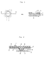
- numeral 1 is a solder bump, numeral 2 a mounting pad, numeral 3 a conductor (conductor circuit), numeral 4 a solder resist, numeral 5 a viahole, numeral 6 an insulating layer, numeral 7 a plated resist (permanent resist), symbol X an opening size of the solder resist, symbol Y an opening size of the viahole, symbol Z a land size of the viahole, symbol ⁇ X a clearance created between an opening edge of the solder resist and an outer peripheral edge of the mounting pad.
- the printed circuit board according to the first example not according to the invention lies in an opening shape of the solder resist so as not to leave the solder resist on the pad as shown in Fig. 3 or a structure that the size of the solder resist is made larger than the size of the mounting pad so as not to overlap the solder resist with the pad.
- Such a structure is not influenced by light scattering or the like produced on the pad surface in the light exposure, so that the curing degree at the boundary between the opening edge of the solder resist and the pad is improved as compared with the conventional structure and hence there can be solved a problem that the gap is created through the development.
- the plating solution sinks into the gap in the Ni/Au plating treatment and the precipitation of plated film proceeds in this portion to cause the peeling in the opening edge of the solder resist.
- the above structure widens the acceptable range of the resolution accompanied with the reduction of the pad size and is not influenced by the light scattering or the like produced on the pad surface in the light exposure, so that it is possible to cope with the mounting in a higher density.
- the printed circuit board is produced by the additive process in which an adhesive layer for electroless plating is formed on a substrate and the surface thereof is roughened and a plated resist and a conductor pattern including a mounting pad is formed on the roughened surface and then the plated resist, mounting pad and conductor pattern are covered with a solder resist, the solder does not contact with the solder resist and the crack hardly occurs.
- the plated resist permanent resist
- the plated resist remains as it is, so that even if the opening size of the solder resist is made large, the flowing of the solder is not caused owing to the step difference between the permanent resist and the mounting pad.
- the structure that the opening size of the solder resist is made larger than the size of the pad is advantageous in case of forming the solder bump through a solder transfer process.
- the solder transfer process is a process wherein a pattern of a solder foil is formed on places corresponding to positions of pads by etching the solder foil attached to a film of a resin such as polyethylene terephthalate or the like and the pattern of the solder foil is placed on the pad so as to contact therewith and heated and reflowed to transfer the solder to the pad.
- the area of the solder foil pattern formed on the film is generally larger than the pad. For this end, when the opening size of the solder resist is made larger than the size of the pad, the solder pattern just fits into the opening portion of the solder resist, which facilitates the positioning in the transfer.
- the clearance created between the opening edge of the solder resist and the outer peripheral edge of the mounting pad is 20-60 ⁇ m.
- the opening portion is formed in the solder resist so as not to overlap with the pad, so that when the clearance is less than 20 ⁇ m, the alignment between the opening portion of the solder resist and the pad portion is difficult.
- the plating solution is apt to remain on the edge of the solder resist.
- the clearance when the clearance is small, the residual plating solution is apt to be applied onto the pad and hence the wettability to the solder is poor in the formation of the solder bump and the connection reliability lowers.
- the clearance when the clearance is more than 60 ⁇ m, it is apt to cause the lowering of wiring density, shortcircuit due to exposure of adjoining pad and the like, and also drawbacks such as solder bridge and the like are apt to be caused due to the formation of enormous solder bump, lateral widening of bump in the mounting of the part and the like.
- the clearance created between the opening edge of the solder resist and the outer peripheral edge of the mounting pad means a gap produced between the opening edge of the solder resist and the outer peripheral edge of the mounting pad.
- the thickness of the solder resist is desirable to be 15-30 ⁇ m.
- the thickness is less than 15 ⁇ m, the effect of the solder resist as a solder dam is not obtained and the shieldability for the wiring circuit lowers. Further, the unevenness of the lower layer is easily affected and there is a fear of exposing the lower layer.
- the problem pointed out in the conventional technique that is, a problem that the curing degree of the lower layer of the solder resist becomes insufficient to cause the floating (peeling) of the solder resist is remarkable when the thickness of the solder resist is not less than 15 ⁇ m. Therefore, the structure according to the invention is particularly effective when the thickness of the solder resist is not less than 1.5 ⁇ m as restricted above.
- the thickness of the solder resist is not more than 30 ⁇ m. Because, in the additive process, the solder resist is formed on the plated (permanent) resist, so that the step difference (between pad surface and upper surface of solder bump) becomes large and the mounting is difficult.
- the printed circuit board according to the first embodiment lies in a point that the position of forming the solder bump is arranged so as to match with the position of the viahole as shown in Fig. 4, particularly a structure that the solder bump is filled in the viahole on the mounting surface and formed so as to cover a portion just above the viahole.
- the viahole is desirable to have a structure that an opening portion is formed so as to pass through the interlaminar insulating layer providing the insulation between the surface layer of conductor circuit and the inner layer of conductor circuit and covered with a metal coating electrically connecting the inner conductor layer to the surface conductor layer in the printed circuit board having a structure of alternately laminating the conductor circuits and the interlaminar insulating layers (second embodiment).
- the inside of the viahole is completely filled with the solder bump.
- the drawbacks such as bubble, unfilled portion and the like remain in the filling of the solder resist.
- the printed circuit board having the above structure according to the invention is also excellent in the electrical connection reliability because the inside of the viahole is completely filled.
- the solder bump is filled and formed in the concave portion of the viahole made from the metal coating.
- the solder bump does not directly contact with the resin of the insulating resin layer, so that there is no breakage of the insulation between the layers or between the patterns due to diffusion of lead even under high-temperature and high-humidity conditions.
- the solder does not close to the resin, so that the peeling is caused when the viahole is made from the solder.
- the solder bump according to the invention contacts with only the metal coating constituting the viahole, so that it is excellent in the adhesion property to the metal coating.
- the solder bump is formed by filling in the concave portion of the viahole, so that the amount of solder used may be made large and it is possible to conduct the accurate mounting of the part through self-alignment effect based on surface tension.
- the metal coatings of nickel and gold are formed on the surface of the viahole according to the invention from the surface side of the viahole. Nickel is excellent in the affinity with copper, while gold is excellent in the affinity with nickel and solder.
- the opening size of the viahole is 50-220 ⁇ m.
- the opening size of the viahole 5 is less than 50 ⁇ m, the size of the solder bump is restricted to a small level and hence the electrical connection reliability to the part is degraded and also the contact area between the viahole and the conductor layer located therebeneath becomes small to degrade the electrical connection reliability to the inner circuit layer.
- the opening size of the viahole exceeds 220 ⁇ m, the solder bump is too large and the drawback such as solder bridge or the like is apt to be caused on the side of the part to be connected, and also it hardly copes with the pitch of the flip chip so as not to obtain the effect of improving the wiring density.
- the land size of the viahole is 80-300 ⁇ m.
- the opening size of the viahole becomes small, the amount of the solder fed may be decreased, but when the land size is less than 80 ⁇ m, the solder bump can not completely be filled in the viahole and formed so as to make higher than the solder resist.
- the land size exceeds 300 ⁇ m, the solder bump is inversely too large and hence the drawbacks such as solder bridge and the like are apt to be caused on the side of the part to be connected and the mounting density and wiring density lower.
- the lowering of the mounting density is caused due to the fact that the mounting area is decreased by the increased portion of the solder bump though the necessary mounting number is unchangeable.
- the printed circuit boards according to the third and fourth embodiment lie in a point that the structure of the solder resist in the example is adopted in the printed circuit board according to the first or second embodiment. According to such a structure, the printed circuit board according to the third or fourth embodiment has the following effects.
- the adhesive for electroless plating is optimum to be obtained by dispersing heat-resistant resin particles soluble in acid or oxidizing agent into heat-resistant resin hardly soluble in acid or oxidizing agent. This is due to the fact that the heat-resistant resin particles soluble in acid or oxidizing agent are roughened and removed, whereby octopus trap-shaped anchors can be formed on the surface to improve the adhesion property to the conductor circuit.
- the adhesive it is desirable that a photosensitized thermosetting resin or a composite of a photosensitized thermosetting resin and a thermoplastic resin is used as the heat-resistant resin hardly soluble in acid or oxidizing agent. Because, the viahole can easily be formed by light exposure and development owing to the photosensitization. Furthermore, the toughness can be improved by compositing with the thermoplastic resin, whereby the improvement of peel strength in the conductor circuit and the prevention of the occurrence of cracks in the viahole portion by heat cycle can be attained.
- an epoxy acrylate obtained by reacting the epoxy resin with acrylic acid, methacrylic acid or the like, and a composite of epoxy acrylate and polyether sulphone.
- the epoxy acrylate it is desirable to react 20-80% of total epoxy group with acrylic acid, methacrylic acid or the like.
- the heat-resistant resin particles is desirable to be selected from 1 heat-resistant resin powder having an average particle size of not more than 10 ⁇ m, 2 agglomerate particles having an average particle size larger by 3 times or more than that of powder and obtained by agglomerating heat-resistant resin powder having an average particle size of not more than 2 ⁇ m, 3 a mixture of heat-resistant resin powder having an average particle size of not more than 10 ⁇ m and heat-resistant resin powder having an average particle size of not more than 1/5 of the particle size of the above powder but not more than 2 ⁇ m, and 4 false particles obtained by adhering at least one of heat-resistant resin powder having an average particle size of not more than 2 ⁇ m and inorganic powder to surfaces of heat-resistant resin powder having an average particle size of 2 ⁇ m - 10 ⁇ m.
- the heat-resistant resin epoxy resin, amino resin (melamine resin, urea resin, guanamine resin) are favorable.
- the solubility of the epoxy resin to acid or oxidizing agent can be changed by varying the kind of oligomer, kind of curing agent and crosslinking density.
- the resin obtained by treating bisphenol A-type epoxy resin oligomer with an amine type curing agent is easily dissolved in the oxidizing agent.
- the resin obtained by treating novolac epoxy resin oligomer with an imidazole type curing agent is hardly dissolved in the oxidizing agent.
- the acid used in the invention there are phosphoric acid, hydrochloric acid, sulfuric acid, and organic acids such as formic acid, acetic acid and so on.
- the organic acid is preferable. Because, when it is subjected to the roughening treatment, it hardly corrodes the metal conductor layer exposed from the viahole.
- the oxidizing agent it is preferable to use chromic acid, permanganate (potassium permanganate or the like). Especially, when the amino resin is dissolved and removed, it is desirable to alternately conduct the roughening treatment with acid and oxidizing agent.
- a plurality of interlaminar insulating layers may be used. For instance, there are the following forms in case of using the plural layers.
- a conductor pattern including a mounting pad 2 as a mounting surface for an electronic part by an additive process is formed on a substrate provided with an inner circuit layer.
- a size of the mounting pad 2 is 100 ⁇ m ⁇ .
- solder resist 4 has a film thickness of 20 ⁇ m and an opening size of 180 ⁇ m.
- a clearance ⁇ X created between an opening edge of the solder resist and an outer peripheral edge of the mounting pad 2 is within a range of 25-55 ⁇ m.
- a conductor pattern including a mounting pad 2 as a mounting surface for an electronic part by an additive process is formed on a substrate provided with an inner circuit layer.
- a size of the mounting pad 2 is 100 ⁇ m ⁇ .
- solder resist 4 has a film thickness of 20 ⁇ m and an opening size of 90 ⁇ m, in which the outer peripheral edge of the pad is overlapped with the opening edge of the solder resist.
- a conductor pattern including a mounting pad 2 as a mounting surface for an electronic part by an additive process is formed on a substrate provided with an inner circuit layer.
- a size of the mounting pad 2 is 100 ⁇ m ⁇ .
- solder resist 4 has a film thickness of 20 ⁇ m and an opening size of 120 ⁇ m.
- a clearance ⁇ X created between an opening edge of the solder resist and an outer peripheral edge of the mounting pad 2 is within a range of 0-20 ⁇ m.
- a conductor pattern including a mounting pad 2 as a mounting surface for an electronic part by an additive process is formed on a substrate provided with an inner circuit layer.
- a size of the mounting pad 2 is 100 ⁇ m ⁇ .
- solder resist 4 has a film thickness of 20 ⁇ m and an opening size of 300 ⁇ m.
- a clearance ⁇ X created between an opening edge of the solder resist and an outer peripheral edge of the mounting pad 2 is within a range of 80-120 ⁇ m.
- a conductor pattern including a mounting pad 2 as a mounting surface for an electronic part by an additive process is formed on a substrate provided with an inner circuit layer.
- a size of the mounting pad 2 is 100 ⁇ m ⁇ .
- solder resist 4 has a film thickness of 10 ⁇ m and an opening size of 180 ⁇ m.
- a clearance ⁇ X created between an opening edge of the solder resist and an outer peripheral edge of the mounting pad 2 is within a range of 25-55 ⁇ m.
- a conductor pattern including a mounting pad 2 as a mounting surface for an electronic part by an additive process is formed on a substrate provided with an inner circuit layer.
- a size of the mounting pad 2 is 100 ⁇ m ⁇ .
- solder resist 4 has a film thickness of 40 ⁇ m and an opening size of 180 ⁇ m.
- a clearance ⁇ X created between an opening edge of the solder resist and an outer peripheral edge of the mounting pad 2 is within a range of 25-55 ⁇ m.
- the mounting pad is subjected to Ni/Au plating of 3 ⁇ m and the solder is fed through screen printing process and then the appearance, resistance to cold-heat shock and insulation property based on the difference of the opening shape in the solder resist are evaluated.
- the results are shown in Table 1.
- Example 1 none more than 1000 cyc O Comparative Example 1 presence 500 cyc ⁇ Comparative Example 2 presence 500 cyc O Comparative Example 3 none more than 1000 cyc x Comparative Example 4 none more than 1000 cyc x Comparative Example 5 presence 500 cyc ⁇ *1 peeling of solder resist; presence or absence of peeling by visual inspection *2 test for resistance to cold-heat shock; time of creating cracks of solder resist in cycle test of -65°C ⁇ 125°C *3 insulation property; electrical insulation to adjacent conductor circuit (including adjacent pad), ⁇ is good and X is poor
- the clearance ⁇ X created between the outer peripheral edge of the pad and the opening edge of the solder resist is larger than the upper limit defined in the invention, so that the adjoining conductor circuit is exposed to cause the electrical shortcircuit in the formation of the solder bump.
- the mounting is possible in a higher density, and no occurrence of bubble is caused in the viahole, and the resistance to cold-heat shock and the connection reliability are excellent.
- Comparative Example 6 in the conventional printed circuit board forming the solder bump 1 by wiring the mounting pad 2 from the viahole 5, bubbles are existent in the resin filled in the viahole 5, so that cracks are apt to be caused in the test for the resistance to cold-heat shock to bring about the degradation of the connection reliability to the part. Further, the wiring density is lowered as compared with Examples 2 and 3 due to the wiring of the mounting pad 2 and hence the formation of higher mounting density (high mounting number) is not attained.
- the bump 1 filled in the viahole 5 can not be formed so as to make higher than the solder resist 4, so that the electrical connection reliability to the part can not be ensured.
- the opening size Y of the viahole 5 is small, the electrical connection reliability between the viahole 5 and the conductor 3 located therebeneath is also poor.
- the printed circuit board according to the invention can easily cope with reductions of weight, thickness and length of substrate and exhibits an excellent adaptability in many fields requiring high performances and high densification of electronic parts.
Landscapes
- Engineering & Computer Science (AREA)
- Microelectronics & Electronic Packaging (AREA)
- Manufacturing & Machinery (AREA)
- Electric Connection Of Electric Components To Printed Circuits (AREA)
- Production Of Multi-Layered Print Wiring Board (AREA)
Claims (5)
- Leiterplatte, die umfasst ein Leitermuster mit einer oberen Leiterschaltung und einer unteren Leiterschaltung und einer dazwischen befindlichen Isolierschicht, und einen Lot-Resist (4), der die obere Leiterschaltung bedeckt, wobei das Leitermuster Kontaktlöcher (5) umfasst, die an einer Montagefläche ausgebildet sind und die Kontaktlöcher (5) aus einem Metallfilm bestehen, der die obere Leiterschaltung elektrisch mit der unteren Leiterschaltung verbindet, dadurch gekennzeichnet, dass eine Größe eines Öffnungsabschnitts, der in dem Lot-Resist (4) ausgebildet ist, größer ist als die Größe der Anschlussfläche (Z) des Durchgangslochs (5), so dass der Lot-Resist (4) nicht von dem Kontaktloch (5) überlappt wird, wobei ein Zwischenraum, der zwischen dem Rand des Öffnungsabschnitts des Lot-Resists (4) und den Außenumfangsrand des Anschlussmaßes des Durchgangslochs (5) erzeugt wird, 20-60 µm beträgt.
- Leiterplatte nach Anspruch 1, wobei der Lot-Resist (4) eine Dicke von 15-30 µm hat.
- Leiterplatte nach Anspruch 1 oder 2, die des Weiteren eine Lötperle (1) umfasst, die in das Kontaktloch (5) gefüllt und darin ausgebildet ist.
- Leiterplatte nach einem der Ansprüche 1 bis 3, wobei die Leiterplatte abwechselnd geschichtete Leiterschaltungen (3) und Zwischen-Isolierschichten (6) aufweist.
- Leiterplatte nach einem der Ansprüche 1 bis 4, wobei das Kontaktloch (5) eine Struktur hat, bei der der Metallfilm, der die obere Leiterschaltung elektrisch mit der unteren Leiterschaltung verbindet, in einer konkaven Öffnung ausgebildet ist, die in der Zwischen-Isolierschicht (6) ausgebildet ist, so dass die Oberfläche der unteren Leiterschicht zu der Oberfläche der Isolierschicht hin frei liegt.
Applications Claiming Priority (5)
| Application Number | Priority Date | Filing Date | Title |
|---|---|---|---|
| JP139501/95 | 1995-06-06 | ||
| JP7139501A JPH08335781A (ja) | 1995-06-06 | 1995-06-06 | 多層プリント配線板 |
| JP14451695A JPH08340173A (ja) | 1995-06-12 | 1995-06-12 | プリント配線板 |
| JP144516/95 | 1995-06-12 | ||
| PCT/JP1996/001539 WO1996039796A1 (en) | 1995-06-06 | 1996-06-06 | Printed wiring board |
Publications (3)
| Publication Number | Publication Date |
|---|---|
| EP0776150A1 EP0776150A1 (de) | 1997-05-28 |
| EP0776150A4 EP0776150A4 (de) | 1999-03-31 |
| EP0776150B1 true EP0776150B1 (de) | 2006-06-07 |
Family
ID=26472294
Family Applications (1)
| Application Number | Title | Priority Date | Filing Date |
|---|---|---|---|
| EP96916328A Expired - Lifetime EP0776150B1 (de) | 1995-06-06 | 1996-06-06 | Gedruckte schaltungsplatte |
Country Status (7)
| Country | Link |
|---|---|
| US (2) | US6291778B1 (de) |
| EP (1) | EP0776150B1 (de) |
| KR (1) | KR100307776B1 (de) |
| CN (1) | CN1080981C (de) |
| DE (1) | DE69636212T2 (de) |
| SG (2) | SG65717A1 (de) |
| WO (1) | WO1996039796A1 (de) |
Families Citing this family (33)
| Publication number | Priority date | Publication date | Assignee | Title |
|---|---|---|---|---|
| JP3050807B2 (ja) | 1996-06-19 | 2000-06-12 | イビデン株式会社 | 多層プリント配線板 |
| JP3050812B2 (ja) | 1996-08-05 | 2000-06-12 | イビデン株式会社 | 多層プリント配線板 |
| US6242079B1 (en) * | 1997-07-08 | 2001-06-05 | Ibiden Co., Ltd. | Printed wiring board and method for manufacturing the same |
| US6141870A (en) | 1997-08-04 | 2000-11-07 | Peter K. Trzyna | Method for making electrical device |
| EP1895586A3 (de) * | 1997-10-17 | 2013-04-03 | Ibiden Co., Ltd. | Substrat für eine Halbleiterpackung |
| WO1999034654A1 (en) * | 1997-12-29 | 1999-07-08 | Ibiden Co., Ltd. | Multilayer printed wiring board |
| KR100906931B1 (ko) | 1998-02-26 | 2009-07-10 | 이비덴 가부시키가이샤 | 필드 바이어 구조를 갖는 다층프린트 배선판 |
| JPH11297889A (ja) | 1998-04-16 | 1999-10-29 | Sony Corp | 半導体パッケージおよび実装基板、ならびにこれらを用いた実装方法 |
| JP2001251040A (ja) * | 2000-03-06 | 2001-09-14 | Stanley Electric Co Ltd | 高周波用回路基板及びその製造方法 |
| JP2001274537A (ja) * | 2000-03-28 | 2001-10-05 | Ngk Spark Plug Co Ltd | 配線基板及び配線基板の製造方法 |
| KR100546695B1 (ko) * | 2000-08-24 | 2006-01-26 | 앰코 테크놀로지 코리아 주식회사 | 반도체 패키지 제조용 가요성 필름 구조 |
| US7759803B2 (en) * | 2001-07-25 | 2010-07-20 | Rohm Co., Ltd. | Semiconductor device and method of manufacturing the same |
| EP1392089A1 (de) * | 2002-08-21 | 2004-02-25 | Ultratera Corporation | Gedruckte Schaltungsplatte mit selbstausrichtenden Bondflächen darauf |
| WO2005086552A1 (ja) * | 2004-03-03 | 2005-09-15 | Shinko Electric Industries Co., Ltd. | 回路基板の製造方法および回路基板 |
| US7190157B2 (en) * | 2004-10-25 | 2007-03-13 | Agilent Technologies, Inc. | Method and apparatus for layout independent test point placement on a printed circuit board |
| JP5050384B2 (ja) * | 2006-03-31 | 2012-10-17 | 富士通セミコンダクター株式会社 | 半導体装置およびその製造方法 |
| US20080123335A1 (en) * | 2006-11-08 | 2008-05-29 | Jong Kun Yoo | Printed circuit board assembly and display having the same |
| JP2008147458A (ja) * | 2006-12-11 | 2008-06-26 | Nec Electronics Corp | プリント配線板およびその製造方法 |
| CN100531527C (zh) * | 2007-01-23 | 2009-08-19 | 李东明 | 印刷电路板掩膜露孔电镀成型工艺 |
| JP2008205132A (ja) * | 2007-02-19 | 2008-09-04 | Nec Corp | プリント配線板及びこれとフレキシブルプリント基板とのはんだ接続構造並びに方法 |
| JP2009246166A (ja) * | 2008-03-31 | 2009-10-22 | Fujitsu Ltd | 電子部品パッケージおよび基板ユニット並びにプリント配線板およびその製造方法 |
| KR101022942B1 (ko) * | 2008-11-12 | 2011-03-16 | 삼성전기주식회사 | 흐름 방지용 댐을 구비한 인쇄회로기판 및 그 제조방법 |
| US8388824B2 (en) * | 2008-11-26 | 2013-03-05 | Enthone Inc. | Method and composition for electrodeposition of copper in microelectronics with dipyridyl-based levelers |
| JP5269563B2 (ja) * | 2008-11-28 | 2013-08-21 | 新光電気工業株式会社 | 配線基板とその製造方法 |
| KR101038235B1 (ko) | 2009-08-31 | 2011-06-01 | 삼성전기주식회사 | 인쇄회로기판 |
| CN101754579B (zh) * | 2009-11-16 | 2012-02-22 | 华为终端有限公司 | 城堡式模块及终端设备 |
| TW201325338A (zh) * | 2011-12-14 | 2013-06-16 | Wistron Corp | 避免金手指結構沾錫之電路板 |
| KR20140086531A (ko) * | 2012-12-28 | 2014-07-08 | 삼성전기주식회사 | 패키지 기판 및 그 제조방법, 그리고 패키지 온 패키지 기판 |
| KR20160010960A (ko) * | 2014-07-21 | 2016-01-29 | 삼성전기주식회사 | 인쇄회로기판 및 그 제조방법 |
| US10515884B2 (en) * | 2015-02-17 | 2019-12-24 | Advanced Semiconductor Engineering, Inc. | Substrate having a conductive structure within photo-sensitive resin |
| US10204889B2 (en) | 2016-11-28 | 2019-02-12 | Taiwan Semiconductor Manufacturing Co., Ltd. | Package structure and method of forming thereof |
| US12069802B2 (en) | 2020-08-07 | 2024-08-20 | Infineon Technologies Ag | Pre-plating of solder layer on solderable elements for diffusion soldering |
| CN115394738A (zh) * | 2022-09-13 | 2022-11-25 | 广东省科学院半导体研究所 | 键合焊点制作方法 |
Family Cites Families (22)
| Publication number | Priority date | Publication date | Assignee | Title |
|---|---|---|---|---|
| US4118595A (en) * | 1977-06-06 | 1978-10-03 | Bell Telephone Laboratories, Incorporated | Crossovers and method of fabrication |
| FR2567709B1 (fr) * | 1984-07-11 | 1990-11-09 | Nec Corp | Ensemble a paillette comprenant un substrat de cablage multi-couche |
| AT389793B (de) | 1986-03-25 | 1990-01-25 | Philips Nv | Leiterplatte fuer gedruckte schaltungen und verfahren zur herstellung solcher leiterplatten |
| US4866507A (en) * | 1986-05-19 | 1989-09-12 | International Business Machines Corporation | Module for packaging semiconductor integrated circuit chips on a base substrate |
| JPH0311792A (ja) | 1989-06-09 | 1991-01-21 | Fujitsu Ltd | はんだバンプの形成方法 |
| JPH045844A (ja) | 1990-04-23 | 1992-01-09 | Nippon Mektron Ltd | Ic搭載用多層回路基板及びその製造法 |
| FR2666173A1 (fr) * | 1990-08-21 | 1992-02-28 | Thomson Csf | Structure hybride d'interconnexion de circuits integres et procede de fabrication. |
| JPH04337695A (ja) | 1991-05-15 | 1992-11-25 | Hitachi Cable Ltd | 多層配線構造体 |
| JPH04354398A (ja) | 1991-05-31 | 1992-12-08 | Internatl Business Mach Corp <Ibm> | 配線基板及びその製造方法 |
| JP2541063Y2 (ja) * | 1991-09-04 | 1997-07-09 | 日本電気株式会社 | プリント基板のパターン構造 |
| JP2658661B2 (ja) | 1991-09-18 | 1997-09-30 | 日本電気株式会社 | 多層印刷配線板の製造方法 |
| JPH0572177U (ja) * | 1992-03-05 | 1993-09-28 | ティーディーケイ株式会社 | 多層基板による回路モジュール |
| JPH05206622A (ja) | 1992-07-23 | 1993-08-13 | Ibiden Co Ltd | プリント配線板 |
| JP2713037B2 (ja) | 1992-07-30 | 1998-02-16 | 凸版印刷株式会社 | プリント配線板及びその製造方法 |
| JPH0669615A (ja) | 1992-08-21 | 1994-03-11 | Ibiden Co Ltd | プリント配線板 |
| JPH07112107B2 (ja) | 1992-12-21 | 1995-11-29 | 日本電気株式会社 | プリント配線板及びその製造方法 |
| JPH06204631A (ja) | 1993-01-08 | 1994-07-22 | Nec Toyama Ltd | 印刷配線板 |
| DE4310930A1 (de) | 1993-04-02 | 1994-10-06 | Siemens Ag | Leiterplattenanordnung und Verfahren zur Herstellung einer bestückten Leiterplatte |
| JPH06350230A (ja) | 1993-06-08 | 1994-12-22 | Fujitsu Ten Ltd | プリント配線基板及びその製造方法 |
| JPH0794885A (ja) | 1993-09-20 | 1995-04-07 | Fujitsu Ltd | 並設プラグイン実装用プリント板の前面板 |
| JP2550881B2 (ja) | 1993-09-27 | 1996-11-06 | 日本電気株式会社 | プリント配線板及びその検査方法 |
| KR0141952B1 (ko) * | 1994-12-19 | 1998-06-01 | 문정환 | 반도체 패키지 및 그 제조방법 |
-
1996
- 1996-06-06 CN CN96190598A patent/CN1080981C/zh not_active Expired - Lifetime
- 1996-06-06 KR KR1019970700629A patent/KR100307776B1/ko not_active Expired - Fee Related
- 1996-06-06 WO PCT/JP1996/001539 patent/WO1996039796A1/ja not_active Ceased
- 1996-06-06 SG SG1997004665A patent/SG65717A1/en unknown
- 1996-06-06 EP EP96916328A patent/EP0776150B1/de not_active Expired - Lifetime
- 1996-06-06 DE DE69636212T patent/DE69636212T2/de not_active Expired - Lifetime
- 1996-06-06 SG SG1998003654A patent/SG71838A1/en unknown
- 1996-06-06 US US08/765,451 patent/US6291778B1/en not_active Expired - Fee Related
-
1998
- 1998-09-11 US US09/152,250 patent/US6303880B1/en not_active Expired - Lifetime
Also Published As
| Publication number | Publication date |
|---|---|
| EP0776150A4 (de) | 1999-03-31 |
| DE69636212D1 (de) | 2006-07-20 |
| SG65717A1 (en) | 1999-06-22 |
| DE69636212T2 (de) | 2007-04-05 |
| CN1155968A (zh) | 1997-07-30 |
| KR970705331A (ko) | 1997-09-06 |
| SG71838A1 (en) | 2000-04-18 |
| US6303880B1 (en) | 2001-10-16 |
| WO1996039796A1 (en) | 1996-12-12 |
| EP0776150A1 (de) | 1997-05-28 |
| CN1080981C (zh) | 2002-03-13 |
| US6291778B1 (en) | 2001-09-18 |
| KR100307776B1 (ko) | 2001-11-22 |
Similar Documents
| Publication | Publication Date | Title |
|---|---|---|
| EP0776150B1 (de) | Gedruckte schaltungsplatte | |
| EP0814643B1 (de) | Mehrschichtige gedruckte Leiterplatte | |
| US6525275B1 (en) | Multilayer printed circuit boards | |
| KR100485628B1 (ko) | 프린트배선판및그의제조방법 | |
| KR100763692B1 (ko) | 다층 회로기판 및 반도체 장치 | |
| US8320135B2 (en) | Multilayer printed circuit board | |
| US8692132B2 (en) | Multilayered printed circuit board and method for manufacturing the same | |
| KR101199807B1 (ko) | 프린트 배선판의 제조 방법 및 프린트 배선판 | |
| US20090027864A1 (en) | Printed circuit board and manufacturing method thereof | |
| US20030168254A1 (en) | Semiconductor chip mounting wiring board, manufacturing method for same, and semiconductor module | |
| JPH10215060A (ja) | プリント配線板の半田バンプ形成方法、その形成方法において使用するプリント配線板および印刷用マスク |
Legal Events
| Date | Code | Title | Description |
|---|---|---|---|
| PUAI | Public reference made under article 153(3) epc to a published international application that has entered the european phase |
Free format text: ORIGINAL CODE: 0009012 |
|
| AK | Designated contracting states |
Kind code of ref document: A1 Designated state(s): DE FI GB NL |
|
| 17P | Request for examination filed |
Effective date: 19970417 |
|
| A4 | Supplementary search report drawn up and despatched | ||
| AK | Designated contracting states |
Kind code of ref document: A4 Designated state(s): DE FI GB NL |
|
| 17Q | First examination report despatched |
Effective date: 20040127 |
|
| GRAP | Despatch of communication of intention to grant a patent |
Free format text: ORIGINAL CODE: EPIDOSNIGR1 |
|
| GRAS | Grant fee paid |
Free format text: ORIGINAL CODE: EPIDOSNIGR3 |
|
| GRAA | (expected) grant |
Free format text: ORIGINAL CODE: 0009210 |
|
| AK | Designated contracting states |
Kind code of ref document: B1 Designated state(s): DE FI GB NL |
|
| REG | Reference to a national code |
Ref country code: GB Ref legal event code: FG4D |
|
| REF | Corresponds to: |
Ref document number: 69636212 Country of ref document: DE Date of ref document: 20060720 Kind code of ref document: P |
|
| PLBE | No opposition filed within time limit |
Free format text: ORIGINAL CODE: 0009261 |
|
| STAA | Information on the status of an ep patent application or granted ep patent |
Free format text: STATUS: NO OPPOSITION FILED WITHIN TIME LIMIT |
|
| 26N | No opposition filed |
Effective date: 20070308 |
|
| PGFP | Annual fee paid to national office [announced via postgrant information from national office to epo] |
Ref country code: DE Payment date: 20120530 Year of fee payment: 17 Ref country code: NL Payment date: 20120626 Year of fee payment: 17 |
|
| PGFP | Annual fee paid to national office [announced via postgrant information from national office to epo] |
Ref country code: GB Payment date: 20120606 Year of fee payment: 17 Ref country code: FI Payment date: 20120612 Year of fee payment: 17 |
|
| REG | Reference to a national code |
Ref country code: NL Ref legal event code: V1 Effective date: 20140101 |
|
| GBPC | Gb: european patent ceased through non-payment of renewal fee |
Effective date: 20130606 |
|
| PG25 | Lapsed in a contracting state [announced via postgrant information from national office to epo] |
Ref country code: FI Free format text: LAPSE BECAUSE OF NON-PAYMENT OF DUE FEES Effective date: 20130606 |
|
| REG | Reference to a national code |
Ref country code: DE Ref legal event code: R119 Ref document number: 69636212 Country of ref document: DE Effective date: 20140101 |
|
| PG25 | Lapsed in a contracting state [announced via postgrant information from national office to epo] |
Ref country code: NL Free format text: LAPSE BECAUSE OF NON-PAYMENT OF DUE FEES Effective date: 20140101 Ref country code: GB Free format text: LAPSE BECAUSE OF NON-PAYMENT OF DUE FEES Effective date: 20130606 Ref country code: DE Free format text: LAPSE BECAUSE OF NON-PAYMENT OF DUE FEES Effective date: 20140101 |