EP0806499A1 - Procédé et dispositif pour la fabrication de semi-conducteurs - Google Patents
Procédé et dispositif pour la fabrication de semi-conducteurs Download PDFInfo
- Publication number
- EP0806499A1 EP0806499A1 EP97303061A EP97303061A EP0806499A1 EP 0806499 A1 EP0806499 A1 EP 0806499A1 EP 97303061 A EP97303061 A EP 97303061A EP 97303061 A EP97303061 A EP 97303061A EP 0806499 A1 EP0806499 A1 EP 0806499A1
- Authority
- EP
- European Patent Office
- Prior art keywords
- evacuation system
- ultra
- liquid nitrogen
- evacuation
- high vacuum
- Prior art date
- Legal status (The legal status is an assumption and is not a legal conclusion. Google has not performed a legal analysis and makes no representation as to the accuracy of the status listed.)
- Granted
Links
- 239000004065 semiconductor Substances 0.000 title claims abstract description 71
- 238000000034 method Methods 0.000 title claims abstract description 67
- IJGRMHOSHXDMSA-UHFFFAOYSA-N Atomic nitrogen Chemical compound N#N IJGRMHOSHXDMSA-UHFFFAOYSA-N 0.000 claims abstract description 130
- 239000007788 liquid Substances 0.000 claims abstract description 69
- 229910052757 nitrogen Inorganic materials 0.000 claims abstract description 65
- 238000004519 manufacturing process Methods 0.000 claims abstract description 46
- 238000001451 molecular beam epitaxy Methods 0.000 claims abstract description 43
- 239000000463 material Substances 0.000 claims abstract description 35
- 238000001704 evaporation Methods 0.000 claims abstract description 7
- OAICVXFJPJFONN-UHFFFAOYSA-N Phosphorus Chemical compound [P] OAICVXFJPJFONN-UHFFFAOYSA-N 0.000 claims description 53
- 229910052698 phosphorus Inorganic materials 0.000 claims description 52
- 239000011574 phosphorus Substances 0.000 claims description 52
- 238000010926 purge Methods 0.000 claims description 31
- 230000008569 process Effects 0.000 claims description 30
- 238000009792 diffusion process Methods 0.000 claims description 5
- 239000000758 substrate Substances 0.000 description 14
- 239000013078 crystal Substances 0.000 description 12
- 229910001218 Gallium arsenide Inorganic materials 0.000 description 9
- 239000011669 selenium Substances 0.000 description 8
- 238000007796 conventional method Methods 0.000 description 7
- 108010083687 Ion Pumps Proteins 0.000 description 6
- BUGBHKTXTAQXES-UHFFFAOYSA-N Selenium Chemical compound [Se] BUGBHKTXTAQXES-UHFFFAOYSA-N 0.000 description 6
- 229910052711 selenium Inorganic materials 0.000 description 6
- XYFCBTPGUUZFHI-UHFFFAOYSA-N Phosphine Chemical compound P XYFCBTPGUUZFHI-UHFFFAOYSA-N 0.000 description 5
- 230000008901 benefit Effects 0.000 description 5
- NINIDFKCEFEMDL-UHFFFAOYSA-N Sulfur Chemical compound [S] NINIDFKCEFEMDL-UHFFFAOYSA-N 0.000 description 4
- 150000004767 nitrides Chemical class 0.000 description 4
- 229910052717 sulfur Inorganic materials 0.000 description 4
- 239000011593 sulfur Substances 0.000 description 4
- 102000006391 Ion Pumps Human genes 0.000 description 3
- 239000007789 gas Substances 0.000 description 3
- 230000010355 oscillation Effects 0.000 description 3
- 229920006395 saturated elastomer Polymers 0.000 description 3
- 238000010521 absorption reaction Methods 0.000 description 2
- 150000001875 compounds Chemical class 0.000 description 2
- 230000007423 decrease Effects 0.000 description 2
- 230000002542 deteriorative effect Effects 0.000 description 2
- 230000002349 favourable effect Effects 0.000 description 2
- 238000004943 liquid phase epitaxy Methods 0.000 description 2
- 229910000073 phosphorus hydride Inorganic materials 0.000 description 2
- 230000009467 reduction Effects 0.000 description 2
- 239000011343 solid material Substances 0.000 description 2
- 229910052799 carbon Inorganic materials 0.000 description 1
- 238000005229 chemical vapour deposition Methods 0.000 description 1
- 238000005253 cladding Methods 0.000 description 1
- 238000000354 decomposition reaction Methods 0.000 description 1
- 238000010438 heat treatment Methods 0.000 description 1
- 230000006872 improvement Effects 0.000 description 1
- 239000012535 impurity Substances 0.000 description 1
- 238000011065 in-situ storage Methods 0.000 description 1
- 238000012423 maintenance Methods 0.000 description 1
- 238000012986 modification Methods 0.000 description 1
- 230000004048 modification Effects 0.000 description 1
- 238000005457 optimization Methods 0.000 description 1
- 230000002093 peripheral effect Effects 0.000 description 1
- 230000000630 rising effect Effects 0.000 description 1
- 239000007787 solid Substances 0.000 description 1
- 239000010409 thin film Substances 0.000 description 1
- 231100000331 toxic Toxicity 0.000 description 1
- 230000002588 toxic effect Effects 0.000 description 1
Images


Classifications
-
- C—CHEMISTRY; METALLURGY
- C30—CRYSTAL GROWTH
- C30B—SINGLE-CRYSTAL GROWTH; UNIDIRECTIONAL SOLIDIFICATION OF EUTECTIC MATERIAL OR UNIDIRECTIONAL DEMIXING OF EUTECTOID MATERIAL; REFINING BY ZONE-MELTING OF MATERIAL; PRODUCTION OF A HOMOGENEOUS POLYCRYSTALLINE MATERIAL WITH DEFINED STRUCTURE; SINGLE CRYSTALS OR HOMOGENEOUS POLYCRYSTALLINE MATERIAL WITH DEFINED STRUCTURE; AFTER-TREATMENT OF SINGLE CRYSTALS OR A HOMOGENEOUS POLYCRYSTALLINE MATERIAL WITH DEFINED STRUCTURE; APPARATUS THEREFOR
- C30B23/00—Single-crystal growth by condensing evaporated or sublimed materials
- C30B23/02—Epitaxial-layer growth
-
- C—CHEMISTRY; METALLURGY
- C23—COATING METALLIC MATERIAL; COATING MATERIAL WITH METALLIC MATERIAL; CHEMICAL SURFACE TREATMENT; DIFFUSION TREATMENT OF METALLIC MATERIAL; COATING BY VACUUM EVAPORATION, BY SPUTTERING, BY ION IMPLANTATION OR BY CHEMICAL VAPOUR DEPOSITION, IN GENERAL; INHIBITING CORROSION OF METALLIC MATERIAL OR INCRUSTATION IN GENERAL
- C23C—COATING METALLIC MATERIAL; COATING MATERIAL WITH METALLIC MATERIAL; SURFACE TREATMENT OF METALLIC MATERIAL BY DIFFUSION INTO THE SURFACE, BY CHEMICAL CONVERSION OR SUBSTITUTION; COATING BY VACUUM EVAPORATION, BY SPUTTERING, BY ION IMPLANTATION OR BY CHEMICAL VAPOUR DEPOSITION, IN GENERAL
- C23C14/00—Coating by vacuum evaporation, by sputtering or by ion implantation of the coating forming material
- C23C14/22—Coating by vacuum evaporation, by sputtering or by ion implantation of the coating forming material characterised by the process of coating
- C23C14/56—Apparatus specially adapted for continuous coating; Arrangements for maintaining the vacuum, e.g. vacuum locks
- C23C14/564—Means for minimising impurities in the coating chamber such as dust, moisture, residual gases
- C23C14/566—Means for minimising impurities in the coating chamber such as dust, moisture, residual gases using a load-lock chamber
Definitions
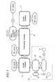
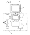
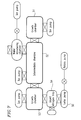
- selenium does not satisfy this condition, selenium deteriorates a degree of vacuum in the vacuum chamber to such an extent that it becomes difficult to evacuate the chamber using an ion pump during a pause in the growth process (specifically, a degree of vacuum deteriorates to 10 -5 torr or higher). Therefore, selenium should be considered to be included with the materials having a high vapor pressure.
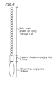
- time required for the step of purging the phosphorus molecules from the liquid nitrogen cold trap 28 can be reduced to about 3 hours from about 20 hours in the conventional technique.
- the operation time of the MBE apparatus required to perform the 20 cycles of the growth process can be reduced from about 100 hours to about 83 hours. Therefore, a productivity can be improved by about 20%.
Landscapes
- Chemical & Material Sciences (AREA)
- Engineering & Computer Science (AREA)
- Materials Engineering (AREA)
- Metallurgy (AREA)
- Organic Chemistry (AREA)
- Chemical Kinetics & Catalysis (AREA)
- Mechanical Engineering (AREA)
- Crystallography & Structural Chemistry (AREA)
- Physical Deposition Of Substances That Are Components Of Semiconductor Devices (AREA)
- Crystals, And After-Treatments Of Crystals (AREA)
- Semiconductor Lasers (AREA)
Applications Claiming Priority (3)
| Application Number | Priority Date | Filing Date | Title |
|---|---|---|---|
| JP11510896 | 1996-05-09 | ||
| JP115108/96 | 1996-05-09 | ||
| JP11510896A JP3555717B2 (ja) | 1996-05-09 | 1996-05-09 | 半導体製造方法 |
Publications (2)
| Publication Number | Publication Date |
|---|---|
| EP0806499A1 true EP0806499A1 (fr) | 1997-11-12 |
| EP0806499B1 EP0806499B1 (fr) | 2001-12-19 |
Family
ID=14654441
Family Applications (1)
| Application Number | Title | Priority Date | Filing Date |
|---|---|---|---|
| EP97303061A Expired - Lifetime EP0806499B1 (fr) | 1996-05-09 | 1997-05-06 | Procédé et dispositif pour la fabrication de semi-conducteurs |
Country Status (4)
| Country | Link |
|---|---|
| US (1) | US6206969B1 (fr) |
| EP (1) | EP0806499B1 (fr) |
| JP (1) | JP3555717B2 (fr) |
| DE (1) | DE69709230T2 (fr) |
Cited By (2)
| Publication number | Priority date | Publication date | Assignee | Title |
|---|---|---|---|---|
| GB2363129A (en) * | 2000-05-04 | 2001-12-12 | Boc Group Plc | Gas supply method and apparatus |
| EP2060662A2 (fr) | 2007-11-16 | 2009-05-20 | Forschungsverbund Berlin E.V. | Dispositif MBE et son procédé de fonctionnement |
Families Citing this family (11)
| Publication number | Priority date | Publication date | Assignee | Title |
|---|---|---|---|---|
| FR2807951B1 (fr) * | 2000-04-20 | 2003-05-16 | Cit Alcatel | Procede et systeme de pompage des chambres de transfert d'equipement de semi-conducteur |
| US6953740B2 (en) * | 2002-03-15 | 2005-10-11 | Cornell Research Foundation, Inc. | Highly doped III-nitride semiconductors |
| US6888170B2 (en) * | 2002-03-15 | 2005-05-03 | Cornell Research Foundation, Inc. | Highly doped III-nitride semiconductors |
| US8231728B2 (en) * | 2003-07-15 | 2012-07-31 | Nippon Mining & Metals Co., Ltd. | Epitaxial growth process |
| DE50309926D1 (de) * | 2003-10-16 | 2008-07-10 | Straumann Holding Ag | Verbessertes Übertragungsteil für ein Implantat |
| US7368368B2 (en) | 2004-08-18 | 2008-05-06 | Cree, Inc. | Multi-chamber MOCVD growth apparatus for high performance/high throughput |
| DE102012104013A1 (de) * | 2012-05-08 | 2013-11-14 | Schmid Vacuum Technology Gmbh | Hochvakuumanlage und Verfahren zum Evakuieren |
| JP6150716B2 (ja) * | 2013-12-02 | 2017-06-21 | 住友重機械工業株式会社 | コールドトラップ |
| US9994956B2 (en) * | 2014-08-11 | 2018-06-12 | University Of Kansas | Apparatus for in situ deposition of multilayer structures via atomic layer deposition and ultra-high vacuum physical or chemical vapor deposition |
| US10593871B2 (en) | 2017-07-10 | 2020-03-17 | University Of Kansas | Atomic layer deposition of ultrathin tunnel barriers |
| US12594619B2 (en) * | 2024-05-03 | 2026-04-07 | Kla Corporation | Systems and methods for ex-situ bakeout of differentially pumped vacuum chambers |
Citations (5)
| Publication number | Priority date | Publication date | Assignee | Title |
|---|---|---|---|---|
| JPS6130664A (ja) * | 1984-07-18 | 1986-02-12 | Rohm Co Ltd | 真空装置の駆動方法 |
| US4664062A (en) * | 1984-10-31 | 1987-05-12 | Hitachi, Ltd. | Apparatus for manufacturing semiconductors |
| JPS63224214A (ja) * | 1987-03-13 | 1988-09-19 | Hitachi Ltd | 分子線エピタキシ装置 |
| JPH03201426A (ja) * | 1989-12-28 | 1991-09-03 | Mitsui Mining & Smelting Co Ltd | 気相分子線エピタキシー装置 |
| EP0510656A2 (fr) * | 1991-04-25 | 1992-10-28 | Hitachi, Ltd. | Système et procédé d'évacuation |
Family Cites Families (3)
| Publication number | Priority date | Publication date | Assignee | Title |
|---|---|---|---|---|
| JP2607239B2 (ja) | 1985-03-29 | 1997-05-07 | シャープ株式会社 | 分子線エピタキシヤル装置 |
| JPS61223608A (ja) | 1985-03-29 | 1986-10-04 | Toshiba Corp | 走行軌跡記録装置 |
| US5447568A (en) * | 1991-12-26 | 1995-09-05 | Canon Kabushiki Kaisha | Chemical vapor deposition method and apparatus making use of liquid starting material |
-
1996
- 1996-05-09 JP JP11510896A patent/JP3555717B2/ja not_active Expired - Fee Related
-
1997
- 1997-05-06 EP EP97303061A patent/EP0806499B1/fr not_active Expired - Lifetime
- 1997-05-06 DE DE69709230T patent/DE69709230T2/de not_active Expired - Fee Related
- 1997-05-09 US US08/853,863 patent/US6206969B1/en not_active Expired - Fee Related
Patent Citations (5)
| Publication number | Priority date | Publication date | Assignee | Title |
|---|---|---|---|---|
| JPS6130664A (ja) * | 1984-07-18 | 1986-02-12 | Rohm Co Ltd | 真空装置の駆動方法 |
| US4664062A (en) * | 1984-10-31 | 1987-05-12 | Hitachi, Ltd. | Apparatus for manufacturing semiconductors |
| JPS63224214A (ja) * | 1987-03-13 | 1988-09-19 | Hitachi Ltd | 分子線エピタキシ装置 |
| JPH03201426A (ja) * | 1989-12-28 | 1991-09-03 | Mitsui Mining & Smelting Co Ltd | 気相分子線エピタキシー装置 |
| EP0510656A2 (fr) * | 1991-04-25 | 1992-10-28 | Hitachi, Ltd. | Système et procédé d'évacuation |
Non-Patent Citations (3)
| Title |
|---|
| PATENT ABSTRACTS OF JAPAN vol. 10, no. 182 (C - 356)<2238> 25 June 1986 (1986-06-25) * |
| PATENT ABSTRACTS OF JAPAN vol. 13, no. 18 (E - 704) 17 January 1989 (1989-01-17) * |
| PATENT ABSTRACTS OF JAPAN vol. 15, no. 465 (E - 1138) 26 November 1991 (1991-11-26) * |
Cited By (3)
| Publication number | Priority date | Publication date | Assignee | Title |
|---|---|---|---|---|
| GB2363129A (en) * | 2000-05-04 | 2001-12-12 | Boc Group Plc | Gas supply method and apparatus |
| EP2060662A2 (fr) | 2007-11-16 | 2009-05-20 | Forschungsverbund Berlin E.V. | Dispositif MBE et son procédé de fonctionnement |
| EP2060662A3 (fr) * | 2007-11-16 | 2010-05-19 | Forschungsverbund Berlin E.V. | Dispositif MBE et son procédé de fonctionnement |
Also Published As
| Publication number | Publication date |
|---|---|
| JP3555717B2 (ja) | 2004-08-18 |
| EP0806499B1 (fr) | 2001-12-19 |
| DE69709230T2 (de) | 2002-07-18 |
| US6206969B1 (en) | 2001-03-27 |
| JPH09298159A (ja) | 1997-11-18 |
| DE69709230D1 (de) | 2002-01-31 |
Similar Documents
| Publication | Publication Date | Title |
|---|---|---|
| US6206969B1 (en) | Method and apparatus for fabricating semiconductor | |
| US4477311A (en) | Process and apparatus for fabricating a semiconductor device | |
| USRE43045E1 (en) | Multi-chamber MOCVD growth apparatus for high performance/high throughput | |
| US5711813A (en) | Epitaxial crystal growth apparatus | |
| JP2009124156A (ja) | Mbe装置及び操作方法 | |
| EP0127200B1 (fr) | Procédé pour la fabrication d'un dispositif semi-conducteur utilisant la technique des faisceaux moléculaires | |
| JP3895410B2 (ja) | Iii−v族窒化物結晶膜を備えた素子、およびその製造方法 | |
| US4622083A (en) | Molecular beam epitaxial process | |
| JP4918221B2 (ja) | 差動真空ポンピングを行う材料蒸発室 | |
| EP0113983A1 (fr) | Fabrication d'un dispositif semi-conducteur au moyen d'épitaxie par faisceau moléculaire | |
| JPS58204899A (ja) | 分子線エピタキシ−装置 | |
| JP3952556B2 (ja) | 分子線エピタキシ装置 | |
| JP2817356B2 (ja) | 分子線結晶成長装置およびそれを用いる結晶成長方法 | |
| CN113710833B (zh) | 直接蒸发泵至冷板的分子束外延系统 | |
| US5741360A (en) | Method of growing a crystal of a compound semiconductor at a low temperature | |
| JP2626516B2 (ja) | 分子線結晶成長装置 | |
| JP4256698B2 (ja) | 多層薄膜製造装置及び製造方法 | |
| JPH0794409A (ja) | Iii−v族化合物半導体薄膜の形成方法 | |
| JPS63220515A (ja) | 半導体層の気相成長方法 | |
| JPS6183700A (ja) | 気相エピタキシヤル成長方法およびその装置 | |
| JPH04219391A (ja) | 分子線結晶成長装置 | |
| JP2005116636A (ja) | 薄膜形成装置 | |
| JPS63204718A (ja) | 有機金属気相成長装置 | |
| JPH033230A (ja) | 半導体気相成長方法 | |
| JPH0794571A (ja) | 半導体プロセス装置及びその使用方法 |
Legal Events
| Date | Code | Title | Description |
|---|---|---|---|
| PUAI | Public reference made under article 153(3) epc to a published international application that has entered the european phase |
Free format text: ORIGINAL CODE: 0009012 |
|
| AK | Designated contracting states |
Kind code of ref document: A1 Designated state(s): DE FR GB |
|
| 17P | Request for examination filed |
Effective date: 19980123 |
|
| 17Q | First examination report despatched |
Effective date: 19991207 |
|
| GRAG | Despatch of communication of intention to grant |
Free format text: ORIGINAL CODE: EPIDOS AGRA |
|
| GRAG | Despatch of communication of intention to grant |
Free format text: ORIGINAL CODE: EPIDOS AGRA |
|
| GRAG | Despatch of communication of intention to grant |
Free format text: ORIGINAL CODE: EPIDOS AGRA |
|
| GRAG | Despatch of communication of intention to grant |
Free format text: ORIGINAL CODE: EPIDOS AGRA |
|
| GRAG | Despatch of communication of intention to grant |
Free format text: ORIGINAL CODE: EPIDOS AGRA |
|
| GRAH | Despatch of communication of intention to grant a patent |
Free format text: ORIGINAL CODE: EPIDOS IGRA |
|
| GRAH | Despatch of communication of intention to grant a patent |
Free format text: ORIGINAL CODE: EPIDOS IGRA |
|
| GRAH | Despatch of communication of intention to grant a patent |
Free format text: ORIGINAL CODE: EPIDOS IGRA |
|
| GRAA | (expected) grant |
Free format text: ORIGINAL CODE: 0009210 |
|
| AK | Designated contracting states |
Kind code of ref document: B1 Designated state(s): DE FR GB |
|
| REG | Reference to a national code |
Ref country code: GB Ref legal event code: IF02 |
|
| REF | Corresponds to: |
Ref document number: 69709230 Country of ref document: DE Date of ref document: 20020131 |
|
| ET | Fr: translation filed | ||
| PLBE | No opposition filed within time limit |
Free format text: ORIGINAL CODE: 0009261 |
|
| STAA | Information on the status of an ep patent application or granted ep patent |
Free format text: STATUS: NO OPPOSITION FILED WITHIN TIME LIMIT |
|
| 26N | No opposition filed | ||
| PGFP | Annual fee paid to national office [announced via postgrant information from national office to epo] |
Ref country code: DE Payment date: 20080515 Year of fee payment: 12 |
|
| PGFP | Annual fee paid to national office [announced via postgrant information from national office to epo] |
Ref country code: GB Payment date: 20080507 Year of fee payment: 12 |
|
| GBPC | Gb: european patent ceased through non-payment of renewal fee |
Effective date: 20090506 |
|
| REG | Reference to a national code |
Ref country code: FR Ref legal event code: ST Effective date: 20100129 |
|
| PG25 | Lapsed in a contracting state [announced via postgrant information from national office to epo] |
Ref country code: FR Free format text: LAPSE BECAUSE OF NON-PAYMENT OF DUE FEES Effective date: 20090602 |
|
| PGFP | Annual fee paid to national office [announced via postgrant information from national office to epo] |
Ref country code: FR Payment date: 20080514 Year of fee payment: 12 |
|
| PG25 | Lapsed in a contracting state [announced via postgrant information from national office to epo] |
Ref country code: GB Free format text: LAPSE BECAUSE OF NON-PAYMENT OF DUE FEES Effective date: 20090506 |
|
| PG25 | Lapsed in a contracting state [announced via postgrant information from national office to epo] |
Ref country code: DE Free format text: LAPSE BECAUSE OF NON-PAYMENT OF DUE FEES Effective date: 20091201 |