EP0823833A2 - Gedruckte Vielschichtschaltungen - Google Patents
Gedruckte Vielschichtschaltungen Download PDFInfo
- Publication number
- EP0823833A2 EP0823833A2 EP97112872A EP97112872A EP0823833A2 EP 0823833 A2 EP0823833 A2 EP 0823833A2 EP 97112872 A EP97112872 A EP 97112872A EP 97112872 A EP97112872 A EP 97112872A EP 0823833 A2 EP0823833 A2 EP 0823833A2
- Authority
- EP
- European Patent Office
- Prior art keywords
- solder
- pads
- pad
- flat
- pad group
- Prior art date
- Legal status (The legal status is an assumption and is not a legal conclusion. Google has not performed a legal analysis and makes no representation as to the accuracy of the status listed.)
- Granted
Links
Images



Classifications
-
- H—ELECTRICITY
- H05—ELECTRIC TECHNIQUES NOT OTHERWISE PROVIDED FOR
- H05K—PRINTED CIRCUITS; CASINGS OR CONSTRUCTIONAL DETAILS OF ELECTRIC APPARATUS; MANUFACTURE OF ASSEMBLAGES OF ELECTRICAL COMPONENTS
- H05K1/00—Printed circuits
- H05K1/02—Details
- H05K1/11—Printed elements for providing electric connections to or between printed circuits
- H05K1/111—Pads for surface mounting, e.g. lay-out
- H05K1/112—Pads for surface mounting, e.g. lay-out directly combined with via connections
-
- H—ELECTRICITY
- H05—ELECTRIC TECHNIQUES NOT OTHERWISE PROVIDED FOR
- H05K—PRINTED CIRCUITS; CASINGS OR CONSTRUCTIONAL DETAILS OF ELECTRIC APPARATUS; MANUFACTURE OF ASSEMBLAGES OF ELECTRICAL COMPONENTS
- H05K3/00—Apparatus or processes for manufacturing printed circuits
- H05K3/30—Assembling printed circuits with electric components, e.g. with resistors
- H05K3/32—Assembling printed circuits with electric components, e.g. with resistors electrically connecting electric components or wires to printed circuits
- H05K3/34—Assembling printed circuits with electric components, e.g. with resistors electrically connecting electric components or wires to printed circuits by soldering
- H05K3/3465—Application of solder
-
- H—ELECTRICITY
- H05—ELECTRIC TECHNIQUES NOT OTHERWISE PROVIDED FOR
- H05K—PRINTED CIRCUITS; CASINGS OR CONSTRUCTIONAL DETAILS OF ELECTRIC APPARATUS; MANUFACTURE OF ASSEMBLAGES OF ELECTRICAL COMPONENTS
- H05K3/00—Apparatus or processes for manufacturing printed circuits
- H05K3/40—Forming printed elements for providing electric connections to or between printed circuits
- H05K3/42—Plated through-holes or plated via connections
- H05K3/429—Plated through-holes specially for multilayer circuits, e.g. having connections to inner circuit layers
-
- H—ELECTRICITY
- H10—SEMICONDUCTOR DEVICES; ELECTRIC SOLID-STATE DEVICES NOT OTHERWISE PROVIDED FOR
- H10W—GENERIC PACKAGES, INTERCONNECTIONS, CONNECTORS OR OTHER CONSTRUCTIONAL DETAILS OF DEVICES COVERED BY CLASS H10
- H10W70/00—Package substrates; Interposers; Redistribution layers [RDL]
- H10W70/60—Insulating or insulated package substrates; Interposers; Redistribution layers
- H10W70/62—Insulating or insulated package substrates; Interposers; Redistribution layers characterised by their interconnections
- H10W70/63—Vias, e.g. via plugs
- H10W70/635—Through-vias
-
- H—ELECTRICITY
- H10—SEMICONDUCTOR DEVICES; ELECTRIC SOLID-STATE DEVICES NOT OTHERWISE PROVIDED FOR
- H10W—GENERIC PACKAGES, INTERCONNECTIONS, CONNECTORS OR OTHER CONSTRUCTIONAL DETAILS OF DEVICES COVERED BY CLASS H10
- H10W70/00—Package substrates; Interposers; Redistribution layers [RDL]
- H10W70/60—Insulating or insulated package substrates; Interposers; Redistribution layers
- H10W70/62—Insulating or insulated package substrates; Interposers; Redistribution layers characterised by their interconnections
- H10W70/65—Shapes or dispositions of interconnections
-
- H—ELECTRICITY
- H10—SEMICONDUCTOR DEVICES; ELECTRIC SOLID-STATE DEVICES NOT OTHERWISE PROVIDED FOR
- H10W—GENERIC PACKAGES, INTERCONNECTIONS, CONNECTORS OR OTHER CONSTRUCTIONAL DETAILS OF DEVICES COVERED BY CLASS H10
- H10W90/00—Package configurations
- H10W90/701—Package configurations characterised by the relative positions of pads or connectors relative to package parts
-
- H—ELECTRICITY
- H05—ELECTRIC TECHNIQUES NOT OTHERWISE PROVIDED FOR
- H05K—PRINTED CIRCUITS; CASINGS OR CONSTRUCTIONAL DETAILS OF ELECTRIC APPARATUS; MANUFACTURE OF ASSEMBLAGES OF ELECTRICAL COMPONENTS
- H05K2201/00—Indexing scheme relating to printed circuits covered by H05K1/00
- H05K2201/09—Shape and layout
- H05K2201/09209—Shape and layout details of conductors
- H05K2201/09372—Pads and lands
- H05K2201/09472—Recessed pad for surface mounting; Recessed electrode of component
-
- H—ELECTRICITY
- H05—ELECTRIC TECHNIQUES NOT OTHERWISE PROVIDED FOR
- H05K—PRINTED CIRCUITS; CASINGS OR CONSTRUCTIONAL DETAILS OF ELECTRIC APPARATUS; MANUFACTURE OF ASSEMBLAGES OF ELECTRICAL COMPONENTS
- H05K2201/00—Indexing scheme relating to printed circuits covered by H05K1/00
- H05K2201/09—Shape and layout
- H05K2201/09209—Shape and layout details of conductors
- H05K2201/095—Conductive through-holes or vias
- H05K2201/09509—Blind vias, i.e. vias having one side closed
-
- H—ELECTRICITY
- H05—ELECTRIC TECHNIQUES NOT OTHERWISE PROVIDED FOR
- H05K—PRINTED CIRCUITS; CASINGS OR CONSTRUCTIONAL DETAILS OF ELECTRIC APPARATUS; MANUFACTURE OF ASSEMBLAGES OF ELECTRICAL COMPONENTS
- H05K2201/00—Indexing scheme relating to printed circuits covered by H05K1/00
- H05K2201/09—Shape and layout
- H05K2201/09818—Shape or layout details not covered by a single group of H05K2201/09009 - H05K2201/09809
- H05K2201/0989—Coating free areas, e.g. areas other than pads or lands free of solder resist
-
- H—ELECTRICITY
- H05—ELECTRIC TECHNIQUES NOT OTHERWISE PROVIDED FOR
- H05K—PRINTED CIRCUITS; CASINGS OR CONSTRUCTIONAL DETAILS OF ELECTRIC APPARATUS; MANUFACTURE OF ASSEMBLAGES OF ELECTRICAL COMPONENTS
- H05K2201/00—Indexing scheme relating to printed circuits covered by H05K1/00
- H05K2201/09—Shape and layout
- H05K2201/09818—Shape or layout details not covered by a single group of H05K2201/09009 - H05K2201/09809
- H05K2201/099—Coating over pads, e.g. solder resist partly over pads
-
- H—ELECTRICITY
- H05—ELECTRIC TECHNIQUES NOT OTHERWISE PROVIDED FOR
- H05K—PRINTED CIRCUITS; CASINGS OR CONSTRUCTIONAL DETAILS OF ELECTRIC APPARATUS; MANUFACTURE OF ASSEMBLAGES OF ELECTRICAL COMPONENTS
- H05K2201/00—Indexing scheme relating to printed circuits covered by H05K1/00
- H05K2201/10—Details of components or other objects attached to or integrated in a printed circuit board
- H05K2201/10613—Details of electrical connections of non-printed components, e.g. special leads
- H05K2201/10621—Components characterised by their electrical contacts
- H05K2201/10734—Ball grid array [BGA]; Bump grid array
-
- H—ELECTRICITY
- H05—ELECTRIC TECHNIQUES NOT OTHERWISE PROVIDED FOR
- H05K—PRINTED CIRCUITS; CASINGS OR CONSTRUCTIONAL DETAILS OF ELECTRIC APPARATUS; MANUFACTURE OF ASSEMBLAGES OF ELECTRICAL COMPONENTS
- H05K2203/00—Indexing scheme relating to apparatus or processes for manufacturing printed circuits covered by H05K3/00
- H05K2203/03—Metal processing
- H05K2203/0338—Transferring metal or conductive material other than a circuit pattern, e.g. bump, solder, printed component
-
- H—ELECTRICITY
- H05—ELECTRIC TECHNIQUES NOT OTHERWISE PROVIDED FOR
- H05K—PRINTED CIRCUITS; CASINGS OR CONSTRUCTIONAL DETAILS OF ELECTRIC APPARATUS; MANUFACTURE OF ASSEMBLAGES OF ELECTRICAL COMPONENTS
- H05K3/00—Apparatus or processes for manufacturing printed circuits
- H05K3/30—Assembling printed circuits with electric components, e.g. with resistors
- H05K3/32—Assembling printed circuits with electric components, e.g. with resistors electrically connecting electric components or wires to printed circuits
- H05K3/34—Assembling printed circuits with electric components, e.g. with resistors electrically connecting electric components or wires to printed circuits by soldering
- H05K3/3452—Solder masks
-
- H—ELECTRICITY
- H05—ELECTRIC TECHNIQUES NOT OTHERWISE PROVIDED FOR
- H05K—PRINTED CIRCUITS; CASINGS OR CONSTRUCTIONAL DETAILS OF ELECTRIC APPARATUS; MANUFACTURE OF ASSEMBLAGES OF ELECTRICAL COMPONENTS
- H05K3/00—Apparatus or processes for manufacturing printed circuits
- H05K3/46—Manufacturing multilayer circuits
- H05K3/4602—Manufacturing multilayer circuits characterized by a special circuit board as base or central core whereon additional circuit layers are built or additional circuit boards are laminated
-
- H—ELECTRICITY
- H05—ELECTRIC TECHNIQUES NOT OTHERWISE PROVIDED FOR
- H05K—PRINTED CIRCUITS; CASINGS OR CONSTRUCTIONAL DETAILS OF ELECTRIC APPARATUS; MANUFACTURE OF ASSEMBLAGES OF ELECTRICAL COMPONENTS
- H05K3/00—Apparatus or processes for manufacturing printed circuits
- H05K3/46—Manufacturing multilayer circuits
- H05K3/4644—Manufacturing multilayer circuits by building the multilayer layer by layer, i.e. build-up multilayer circuits
-
- H—ELECTRICITY
- H10—SEMICONDUCTOR DEVICES; ELECTRIC SOLID-STATE DEVICES NOT OTHERWISE PROVIDED FOR
- H10W—GENERIC PACKAGES, INTERCONNECTIONS, CONNECTORS OR OTHER CONSTRUCTIONAL DETAILS OF DEVICES COVERED BY CLASS H10
- H10W70/00—Package substrates; Interposers; Redistribution layers [RDL]
- H10W70/60—Insulating or insulated package substrates; Interposers; Redistribution layers
- H10W70/62—Insulating or insulated package substrates; Interposers; Redistribution layers characterised by their interconnections
- H10W70/65—Shapes or dispositions of interconnections
- H10W70/654—Top-view layouts
- H10W70/655—Fan-out layouts
-
- H—ELECTRICITY
- H10—SEMICONDUCTOR DEVICES; ELECTRIC SOLID-STATE DEVICES NOT OTHERWISE PROVIDED FOR
- H10W—GENERIC PACKAGES, INTERCONNECTIONS, CONNECTORS OR OTHER CONSTRUCTIONAL DETAILS OF DEVICES COVERED BY CLASS H10
- H10W72/00—Interconnections or connectors in packages
- H10W72/071—Connecting or disconnecting
- H10W72/072—Connecting or disconnecting of bump connectors
- H10W72/07251—Connecting or disconnecting of bump connectors characterised by changes in properties of the bump connectors during connecting
-
- H—ELECTRICITY
- H10—SEMICONDUCTOR DEVICES; ELECTRIC SOLID-STATE DEVICES NOT OTHERWISE PROVIDED FOR
- H10W—GENERIC PACKAGES, INTERCONNECTIONS, CONNECTORS OR OTHER CONSTRUCTIONAL DETAILS OF DEVICES COVERED BY CLASS H10
- H10W72/00—Interconnections or connectors in packages
- H10W72/20—Bump connectors, e.g. solder bumps or copper pillars; Dummy bumps; Thermal bumps
Definitions
- the present invention relates to a multilayer printed circuit board, and more particularly to a multilayer printed circuit board for the mounting of flip chips capable of reducing the number of wiring layers while maintaining high density packaging property on a surface of a wiring substrate.
- a group of solder pads formed by arranging many pads each provided with a solder bump is formed on a mounting surface.
- the solder pad group is constructed solder pads having a structure that sphere-shaped solder is formed on a surface of a flat and disc-shaped conductor called as a mounting pad (or land) electrically connected to a given conductor pattern of a wiring substrate through surface tension, which is electrically connected, for example, to an external terminal for mounting a package onto a mother board or the like through given wiring drawn from the mounting pad.
- solder pads located in an inner side of the solder pad group are required to electrically connect the conductor pattern connected to the mounting pad through wirings drawn from pads, which are located outside the mounting pads at a biased state, to the external terminals. Therefore, the distance between the pads located near to the outer periphery of the wiring substrate is required to surely take a region corresponding to the width of the wiring and hence there is caused a problem of making the high integration of electronic components (chips) difficult.
- the wiring pattern is made fine and hence the frequency of causing failure places becomes high.
- the buildup wiring board forming the wiring layers every one layer it is difficult to confirm the failure in the production course, so that if the failure is caused even at one place in each wiring layer, the wiring board as a final product becomes failure and the good laminated material should be disposed and hence there is a problem of facilitating the deterioration of production efficiency and production yield.
- the multilayer printed circuit board for mounting flip chips is particularly manufactured by the buildup method, it is necessary to attain the high integration of electronic components and at the same time the reduction of the wiring layer number in order to cope with the mass production without deteriorating the production efficiency and the production yield.
- an object of the invention to provide a multilayer printed circuit board for mounting flip chips which can realize high integration (high densification) of solder pads and reduce the number of wiring layers while maintaining high density packaging property on a surface of wiring substrate.
- the inventor has made various studies in order to achieve the above object and as a result the invention has been accomplished.
- a multilayer printed wiring board comprising a core substrate, multilayer wiring layers formed thereon by alternately laminating interlaminar insulating layers and conductor circuits and a solder pad group formed by two-dimensionally arranging pads provided with solder bumps on the surface of the multilayer wiring layer, characterized in that the solder pads of the solder pad group are arranged in only a peripheral portion other than a central portion to form a frame shape and the solder pads located at the outside part among the frame-shaped solder pad group are constructed with flat pads each connected to conductor pattern on their surface and solder bumps formed on the surfaces of the flat pads, while the solder pads located at the inside part are constructed with viaholes each connected to an innerlayer flat pad group located in an innerlayer and solder bumps formed in recess portions of these viaholes.
- the solder pads located at the outside part of the solder pad group are solder pads located in first to fifth rows viewed from the outermost periphery, and it is desirable that the interlaminar insulating layer has a roughened surface having a surface roughness of 5-15 ⁇ m.
- solder resist layer is formed on the multilayer wiring layer and an opening size of the solder resist is made larger than a diameter of each of the flat pad constituting the and the viahole so as not to overlap the solder resist with the flat pad or the viahole.
- the invention proposes a new structure of the solder pad group in the multilayer printed circuit board for mounting flip chips comprising the core substrate, the multilayer wiring layer formed by alternately laminating the interlaminar insulating layers and the conductor circuits and the solder pad group formed by two-dimensionally arranging pads provided with solder bumps on the surface of the multilayer wiring layer.
- two-dimensionally arrangement includes not only a method of arranging pads in form of network in X-Y directions as shown in Fig. 2(a) but also a method of arranging pads zigzag in X-Y directions as shown in Fig. 2(b).
- the zigzag arranging form is advantageous in a point that the wiring can easily be drawn out from the inside pad toward the external terminal.
- the invention is optimum to have a structure that the arrangement of the solder pad group takes a zigzag form as shown in Fig. 1(b) and the solder pads located from the outermost row to a third row in the solder pad group are connected to conductor patterns on the surface of the multilayer wiring layer.
- the conductor patterns to be connected to the pads of the second and third rows are arranged so as to divide a distance between the pads of the outermost row (first row) into three equal parts and further the conductor patterns to be connected to the pads of the third row are arranged so as to divide a distance between the pad of the first row and the pad of the second row into tow equal parts.
- the multilayer printed circuit board according to the invention lies in a structure that the shape of the solder pad group formed on the surface of the multilayer wiring layer is a frame (ring) arranging the pads in only a peripheral portion other than a central portion and the solder pads located on outer portion among the frame-shaped solder pad group, desirably solder pads located from an outermost row to fifth row are constructed with flat pads connected to conductor patterns on the surface and solder bumps formed on the flat pads, while the solder pads located in the inside portion other than the above solder pads are constituted with viaholes connected to flat innerlayer pad group located in the inner layer and solder bumps formed in recess portions of the viaholes.
- the flat pads located from the first to fifth rows among the solder pads of the solder pad group are connected to the conductor patterns on the surface and electrically connected to external terminals located outside of the solder pad group through wirings drawn out from these pads.
- the pads other than the solder pads located from first to fifth rows are connected to the flat innerlayer pad group located in the inner layer through the viaholes and electrically connected to the external terminals located outside the pad group through the wirings drawn out from the innerlayer pads.
- the conductor patterns connected to the pads located from the first to fifth rows in the solder pad group are connected to the external terminals through the wirings drawn out from the pads detouring the pads of first to fourth rows and the pads other than the above are viaholes connected to the innerlayer pads and also connected to the external terminals through the wirings drawn out from the innerlayer pads.
- the structure that the wirings connected to the solder pads located in the inside of the solder pad group are divided from the innerlayer pads and drawn out therefrom is used instead of the conventional structure that all wirings for connecting to the external terminals are drawn out from the solder pad group on the surface, so that the distance between the solder pads on the surface layer can be decreased and hence the high densification (high integration) of the solder pads can be attained.
- the shape of the solder pad group formed on the surface of the multilayer wiring layer is rendered into a frame (ring) arranging the pads in only the peripheral portion other than the central portion, whereby the reduction of the wiring layer number can be attained while maintaining the high density mounting property of the surface of the wiring substrate.
- the shape of the solder pad group is a full grid matrix as shown in Fig. 3, in order to maintain the high density packaging property on the surface of the wiring substrate, it is necessary that the solder pads located toward the central portion are sequentially divided and connected to each innerlayer pad group as an under layer through the viaholes and finally connected to the innerlayer pad group on the core substrate. In this shape, therefore, it is required to use the wiring layer for dividing into innerlayer pad groups, so that the wiring layer number can not be decreased while maintaining the high density packaging property on the surface of the wiring substrate.
- the shape of the solder pad group is a frame form arranging the pads in only a peripheral portion other than the central portion as shown in Fig.
- the solder pad is not existent in the central portion, so that the number of the wiring layers for dividing into innerlayer pad groups can be decreased by the number corresponding to the row number in the central portion existing no solder pad.
- the lacking number of solder pads located in the central portion is compensated by increasing the row number at the outside of the solder pad group.
- the increase of the row number at the outside of the solder pad group is less in the lacking row number in the central portion. In the shape of the solder pad group according to the invention, therefore, it is possible to reduce the number of the wiring layers while maintaining a high density packaging property on the surface of the wiring substrate.
- the invention it is possible to reduce the number of the wiring layers while maintaining the sufficient solder pad number by increasing only the two outer circumferential rows per a side as compared with 8 rows removed from the central portion. Furthermore, the row number is increased only by two rows, so that it is not difficult to arrange conductor patterns drawn out for connecting to external terminals and the like, and also the density of the solder pads is not lowered.
- the shape of the solder pad group arranged in the frame shape is a square shape
- the shape may be rectangular, circular or polygonal such as octagonal or the like as shown in Fig. 9.
- the detouring of the conductor patterns drawn out for connecting the solder pads at corner part to the external terminal or the like is becomes less as compared with the case of rectangular or square shape.
- pads consisting of plural viaholes for adjusting the number of solder pads can be formed in the central portion existing no solder bump.
- solder pads located in the inside portion in the frame-shaped solder pad group desirably solder pads other than the solder pads located inward from the first to fifth rows are a combination of viaholes connected to flat innerlayer pad group located in an inner layer and solder bumps formed in recess portions of the viaholes.
- the viahole according to the invention has a structure that a metal film for electrically connecting the innerlayer pad to the conductor circuit on the surface of the interlaminar insulating layer is formed in an opening portion formed in the interlaminar insulating layer so as to expose the innerlayer pad.
- a metal film for electrically connecting the innerlayer pad to the conductor circuit on the surface of the interlaminar insulating layer is formed in an opening portion formed in the interlaminar insulating layer so as to expose the innerlayer pad.
- the viahole is made from the metal film and the solder is filled in the recess portion of the viahole, so that there is caused no degradation of the resin nor falling down of the viahole.
- the conductor patterns of the multilayer wiring layer connected to the above pad group are connected to external terminals arranged on the rear surface of the core substrate such as solder bumps, conductor pins and the like through the through-holes formed in the core substrate.
- the multilayer wiring layer formed by alternately laminating the conductor layers and the insulating resin layers for electrically connecting to the through-holes as formed in the rear surface of the core substrate and the solder bumps are formed on the surface thereof (see Fig. 1).
- the viaholes constituting the solder pad group are apt to be peeled off because they are connected only to the innerlayer pads.
- a roughened surface having a surface roughness of 5-15 ⁇ m is formed on the interlaminar insulating layer.
- the surface roughness is less than 5 ⁇ m, the adhesion strength to the viahole is insufficient, while when it exceeds 15 ⁇ m, it is difficult to obtain fine conductor patterns.
- the solder resist layer is formed on the surface of the multilayer wiring layer.
- the opening size of the solder resist is made larger than the diameter of the flat pad constituting the solder pad or the viahole so as not to overlap the solder resist with the pad or viahole, whereby the pad and viahole are completely exposed from the openings of the solder resists.
- the opening size of the solder resist is made smaller than the diameter of the pad
- the opening is formed by subjecting the solder resist of the photosensitive resin to a light exposure development (so-called photolithography)
- the position shifting of the opening portion is caused by temperature expansion and shrinkage of the photomask and hence the exposure area of the pad is substantially decreased.
- problems such as flowing of solder, solder bridge and the like are apt to be created and the mounting reliability of the component becomes poor.
- the solder pad group other than the solder pads located at the outside of the frame-shaped solder pad group are constituted with solder bumps formed in the recess portions of the viaholes, so that they are never connected to the conductor patterns located in the same layer.
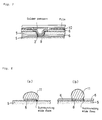
- the pads for the formation of solder bumps are not newly wired from the viaholes, so that even when the opening size of the solder resist is made larger than the diameter of the viahole, the wiring of the conductor pattern is not exposed from the opening portion of the solder resist (see Fig. 6(a)). Therefore, when the solder bump is formed in the recess portion of the viahole according to the invention, the lowering of the solder bump is not caused and also the position shifting of the solder bump is not caused (see Fig. 6(b)).
- the structure that the opening size of the solder resist is made larger than the diameter of the pad is particularly advantageous when the solder bump is formed by solder transferring method.
- the solder transferring method is carried out by etching a solder foil attached onto a film to form patterns of solder foil at places corresponding to positions of pads, placing the patterned solder foil so as to contact with the pads and reflowing under heating to transfer the solder onto the pads because the solder is not drapable with the film but is drapable with metal.
- an area of solder foil pattern formed on the film is generally larger than the pad. Therefore, when the opening size of the solder resist is made larger than the diameter of the pad, the solder pattern is just fitted into the opening portion of the solder resist to easily conduct the positioning thereof (see Fig. 7).
- the wiring layer located as an outermost layer is formed by flat pads and viaholes between plating resists through the plating resist and a solder resist layer having opening portions for exposing the flat pads and viaholes is formed on the surface thereof. It is advantageous that the opening size of the solder resist layer is made larger than the diameter of the pad or the viahole to expose a part of the pads, viaholes and the plating resist.
- cracks may be generated in the interlaminar insulating resin layer (the adhesive layer for electroless plating) starting from a boundary between the plating resist and the conductor pattern.
- the opening size of the solder resist layer is made smaller than the diameter of the flat pad or the viahole so as to overlap the solder resist with the pad or the viahole as shown in Fig. 10.
- the multilayer printed circuit board is manufactured by the semi-additive process, a plating resist is not existent in the multilayer printed circuit board, so that the peeling of the solder is apt to be caused.
- the opening size of the solder resist is made smaller than the diameter of the flat pad or the viahole, the peeling of the solder pad can be prevented.
- the thus obtained multilayer printed circuit board is diagrammatically shown in Fig. 1.
- This multilayer printed circuit board has also multilayer wiring layers at the back side, which are fundamentally produced in the same manner as described above.
- a semi-additive process may be adopted in addition to the full additive process as the method of producing the multilayer printed circuit board.
- the semi-additive process is a method wherein a surface of an interlaminar insulating resin layer is roughened and subjected to an electroless plating of a thin thickness over a full surface and a plating resist is formed on a portion of the electroless plated film not forming conductor and a portion not forming the resist is subjected to an electrolytic plating of a thick thickness and then the plating resist and the electroless plated film located therebelow are removed to form a conductor circuit pattern.
- multilayer printed circuit boards for the mounting of flip chips capable of attaining the high integration (high densification) of solder pads and reducing the number of wiring layers while maintaining a high density mounting property of wiring substrate surface.
Landscapes
- Engineering & Computer Science (AREA)
- Microelectronics & Electronic Packaging (AREA)
- Manufacturing & Machinery (AREA)
- Production Of Multi-Layered Print Wiring Board (AREA)
- Printing Elements For Providing Electric Connections Between Printed Circuits (AREA)
- Non-Metallic Protective Coatings For Printed Circuits (AREA)
Applications Claiming Priority (2)
| Application Number | Priority Date | Filing Date | Title |
|---|---|---|---|
| JP8206170A JP3050812B2 (ja) | 1996-08-05 | 1996-08-05 | 多層プリント配線板 |
| JP206170/96 | 1996-08-05 |
Publications (3)
| Publication Number | Publication Date |
|---|---|
| EP0823833A2 true EP0823833A2 (de) | 1998-02-11 |
| EP0823833A3 EP0823833A3 (de) | 1999-04-14 |
| EP0823833B1 EP0823833B1 (de) | 2008-09-24 |
Family
ID=16518972
Family Applications (1)
| Application Number | Title | Priority Date | Filing Date |
|---|---|---|---|
| EP97112872A Expired - Lifetime EP0823833B1 (de) | 1996-08-05 | 1997-07-25 | Lötpad-Anordnung und Verbindungsstruktur für mehrlagige Leiterplatten |
Country Status (8)
| Country | Link |
|---|---|
| US (1) | US6525275B1 (de) |
| EP (1) | EP0823833B1 (de) |
| JP (1) | JP3050812B2 (de) |
| KR (1) | KR100276802B1 (de) |
| CN (1) | CN1082783C (de) |
| DE (1) | DE69739005D1 (de) |
| MY (1) | MY118245A (de) |
| SG (1) | SG71716A1 (de) |
Cited By (7)
| Publication number | Priority date | Publication date | Assignee | Title |
|---|---|---|---|---|
| WO2000022894A1 (en) * | 1998-10-13 | 2000-04-20 | Sun Microsystems, Inc. | Apparatus and system with increased signal trace routing options in printed wiring boards and integrated circuit packaging |
| EP0883173A4 (de) * | 1996-09-12 | 2001-05-09 | Ibiden Co Ltd | Leiterplatte zur montage elektronischer bauelemente |
| US6384344B1 (en) | 1995-06-19 | 2002-05-07 | Ibiden Co., Ltd | Circuit board for mounting electronic parts |
| WO2004002203A1 (ja) * | 2002-06-25 | 2003-12-31 | Nec Corporation | 回路基板装置および基板間の接続方法 |
| WO2003049183A3 (en) * | 2001-12-04 | 2004-01-22 | Koninkl Philips Electronics Nv | Optimum power and ground bump pad and bump patterns for flip chip packaging |
| EP1605739A4 (de) * | 2003-04-18 | 2009-08-19 | Ibiden Co Ltd | Leiterplatte mit starrer nachgiebigkeit |
| US8093502B2 (en) | 2004-06-10 | 2012-01-10 | Ibiden Co., Ltd. | Flex-rigid wiring board and manufacturing method thereof |
Families Citing this family (20)
| Publication number | Priority date | Publication date | Assignee | Title |
|---|---|---|---|---|
| US6141870A (en) | 1997-08-04 | 2000-11-07 | Peter K. Trzyna | Method for making electrical device |
| WO2000018202A1 (en) * | 1998-09-17 | 2000-03-30 | Ibiden Co., Ltd. | Multilayer build-up wiring board |
| JP4832621B2 (ja) * | 1999-10-26 | 2011-12-07 | イビデン株式会社 | 多層プリント配線板 |
| CN1199536C (zh) | 1999-10-26 | 2005-04-27 | 伊比登株式会社 | 多层印刷配线板及多层印刷配线板的制造方法 |
| US6815621B2 (en) * | 2000-10-02 | 2004-11-09 | Samsung Electronics Co., Ltd. | Chip scale package, printed circuit board, and method of designing a printed circuit board |
| US6732908B2 (en) * | 2002-01-18 | 2004-05-11 | International Business Machines Corporation | High density raised stud microjoining system and methods of fabricating the same |
| JP2004140313A (ja) * | 2002-08-22 | 2004-05-13 | Jsr Corp | 二層積層膜を用いた電極パッド上へのバンプ形成方法 |
| WO2005081312A1 (ja) * | 2004-02-24 | 2005-09-01 | Ibiden Co., Ltd. | 半導体搭載用基板 |
| US7303941B1 (en) * | 2004-03-12 | 2007-12-04 | Cisco Technology, Inc. | Methods and apparatus for providing a power signal to an area array package |
| JP2007142124A (ja) * | 2005-11-18 | 2007-06-07 | Matsushita Electric Ind Co Ltd | 半導体装置およびその製造方法 |
| US20070246158A1 (en) * | 2006-04-21 | 2007-10-25 | 3M Innovative Properties Company | Wiring board, production process thereof and connection method using same |
| TWI315658B (en) * | 2007-03-02 | 2009-10-01 | Phoenix Prec Technology Corp | Warp-proof circuit board structure |
| US7982504B1 (en) | 2010-01-29 | 2011-07-19 | Hewlett Packard Development Company, L.P. | Interconnection architecture for multilayer circuits |
| US9324718B2 (en) | 2010-01-29 | 2016-04-26 | Hewlett Packard Enterprise Development Lp | Three dimensional multilayer circuit |
| USD675171S1 (en) * | 2010-12-16 | 2013-01-29 | Tecella Llc | Multi-electrode holder |
| US20130168132A1 (en) * | 2011-12-29 | 2013-07-04 | Sumsung Electro-Mechanics Co., Ltd. | Printed circuit board and method of manufacturing the same |
| JP2013219144A (ja) * | 2012-04-06 | 2013-10-24 | Sumitomo Electric Printed Circuit Inc | フレキシブルプリント配線板及びフレキシブルプリント配線板の製造方法 |
| JP5502139B2 (ja) * | 2012-05-16 | 2014-05-28 | 日本特殊陶業株式会社 | 配線基板 |
| KR102214512B1 (ko) | 2014-07-04 | 2021-02-09 | 삼성전자 주식회사 | 인쇄회로기판 및 이를 이용한 반도체 패키지 |
| CN115226323A (zh) * | 2022-06-17 | 2022-10-21 | 上海泽丰半导体科技有限公司 | 低温共烧陶瓷基板表面焊盘及其制备方法 |
Family Cites Families (20)
| Publication number | Priority date | Publication date | Assignee | Title |
|---|---|---|---|---|
| JPS6155994A (ja) * | 1984-08-27 | 1986-03-20 | 信越化学工業株式会社 | 銅張りフレキシブルプリント回路用基板 |
| US4866507A (en) | 1986-05-19 | 1989-09-12 | International Business Machines Corporation | Module for packaging semiconductor integrated circuit chips on a base substrate |
| JPH0311792A (ja) | 1989-06-09 | 1991-01-21 | Fujitsu Ltd | はんだバンプの形成方法 |
| JPH0744320B2 (ja) * | 1989-10-20 | 1995-05-15 | 松下電器産業株式会社 | 樹脂回路基板及びその製造方法 |
| DE69229661T2 (de) | 1991-04-26 | 1999-12-30 | Citizen Watch Co., Ltd. | Verfahren zur Herstellung einer Anschlusstruktur für eine Halbleiteranordnung |
| JPH04337695A (ja) | 1991-05-15 | 1992-11-25 | Hitachi Cable Ltd | 多層配線構造体 |
| US5355019A (en) | 1992-03-04 | 1994-10-11 | At&T Bell Laboratories | Devices with tape automated bonding |
| US5473120A (en) * | 1992-04-27 | 1995-12-05 | Tokuyama Corporation | Multilayer board and fabrication method thereof |
| JP2713037B2 (ja) | 1992-07-30 | 1998-02-16 | 凸版印刷株式会社 | プリント配線板及びその製造方法 |
| JP2988603B2 (ja) | 1992-08-20 | 1999-12-13 | 株式会社豊田自動織機製作所 | 半導体パッケージ |
| JPH0669615A (ja) | 1992-08-21 | 1994-03-11 | Ibiden Co Ltd | プリント配線板 |
| JPH07112107B2 (ja) | 1992-12-21 | 1995-11-29 | 日本電気株式会社 | プリント配線板及びその製造方法 |
| JPH06350230A (ja) | 1993-06-08 | 1994-12-22 | Fujitsu Ten Ltd | プリント配線基板及びその製造方法 |
| JP2550881B2 (ja) | 1993-09-27 | 1996-11-06 | 日本電気株式会社 | プリント配線板及びその検査方法 |
| US5487218A (en) * | 1994-11-21 | 1996-01-30 | International Business Machines Corporation | Method for making printed circuit boards with selectivity filled plated through holes |
| KR0141952B1 (ko) | 1994-12-19 | 1998-06-01 | 문정환 | 반도체 패키지 및 그 제조방법 |
| US5798909A (en) * | 1995-02-15 | 1998-08-25 | International Business Machines Corporation | Single-tiered organic chip carriers for wire bond-type chips |
| TW373308B (en) * | 1995-02-24 | 1999-11-01 | Agere Systems Inc | Thin packaging of multi-chip modules with enhanced thermal/power management |
| CN1080981C (zh) | 1995-06-06 | 2002-03-13 | 揖斐电株式会社 | 印刷电路板 |
| US5710071A (en) * | 1995-12-04 | 1998-01-20 | Motorola, Inc. | Process for underfilling a flip-chip semiconductor device |
-
1996
- 1996-08-05 JP JP8206170A patent/JP3050812B2/ja not_active Expired - Fee Related
-
1997
- 1997-07-21 US US08/897,702 patent/US6525275B1/en not_active Expired - Lifetime
- 1997-07-25 EP EP97112872A patent/EP0823833B1/de not_active Expired - Lifetime
- 1997-07-25 DE DE69739005T patent/DE69739005D1/de not_active Expired - Lifetime
- 1997-07-26 MY MYPI97003418A patent/MY118245A/en unknown
- 1997-07-31 KR KR1019970036339A patent/KR100276802B1/ko not_active Expired - Fee Related
- 1997-08-01 SG SG1997002759A patent/SG71716A1/en unknown
- 1997-08-04 CN CN97115322A patent/CN1082783C/zh not_active Expired - Fee Related
Cited By (12)
| Publication number | Priority date | Publication date | Assignee | Title |
|---|---|---|---|---|
| US6384344B1 (en) | 1995-06-19 | 2002-05-07 | Ibiden Co., Ltd | Circuit board for mounting electronic parts |
| EP0883173A4 (de) * | 1996-09-12 | 2001-05-09 | Ibiden Co Ltd | Leiterplatte zur montage elektronischer bauelemente |
| EP1397031A3 (de) * | 1996-09-12 | 2005-01-19 | Ibiden Co., Ltd. | Leiterplatte zur Montage von elektronischen Bauelementen |
| USRE44251E1 (en) | 1996-09-12 | 2013-06-04 | Ibiden Co., Ltd. | Circuit board for mounting electronic parts |
| WO2000022894A1 (en) * | 1998-10-13 | 2000-04-20 | Sun Microsystems, Inc. | Apparatus and system with increased signal trace routing options in printed wiring boards and integrated circuit packaging |
| US6534872B1 (en) | 1998-10-13 | 2003-03-18 | Sun Microsystems, Inc. | Apparatus and system with increased signal trace routing options in printed wiring boards and integrated circuit packaging |
| WO2003049183A3 (en) * | 2001-12-04 | 2004-01-22 | Koninkl Philips Electronics Nv | Optimum power and ground bump pad and bump patterns for flip chip packaging |
| WO2004002203A1 (ja) * | 2002-06-25 | 2003-12-31 | Nec Corporation | 回路基板装置および基板間の接続方法 |
| US7501584B2 (en) | 2002-06-25 | 2009-03-10 | Nec Corporation | Circuit board device and method for board-to-board connection |
| EP1605739A4 (de) * | 2003-04-18 | 2009-08-19 | Ibiden Co Ltd | Leiterplatte mit starrer nachgiebigkeit |
| US7655869B2 (en) | 2003-04-18 | 2010-02-02 | Ibiden Co., Ltd. | Flex-rigid wiring board |
| US8093502B2 (en) | 2004-06-10 | 2012-01-10 | Ibiden Co., Ltd. | Flex-rigid wiring board and manufacturing method thereof |
Also Published As
| Publication number | Publication date |
|---|---|
| MY118245A (en) | 2004-09-30 |
| JPH1051146A (ja) | 1998-02-20 |
| KR19980018258A (ko) | 1998-06-05 |
| SG71716A1 (en) | 2000-04-18 |
| US6525275B1 (en) | 2003-02-25 |
| EP0823833B1 (de) | 2008-09-24 |
| KR100276802B1 (ko) | 2001-02-01 |
| EP0823833A3 (de) | 1999-04-14 |
| CN1173108A (zh) | 1998-02-11 |
| CN1082783C (zh) | 2002-04-10 |
| JP3050812B2 (ja) | 2000-06-12 |
| DE69739005D1 (de) | 2008-11-06 |
Similar Documents
| Publication | Publication Date | Title |
|---|---|---|
| EP0823833B1 (de) | Lötpad-Anordnung und Verbindungsstruktur für mehrlagige Leiterplatten | |
| EP0814643B1 (de) | Mehrschichtige gedruckte Leiterplatte | |
| EP0776150B1 (de) | Gedruckte schaltungsplatte | |
| US7957154B2 (en) | Multilayer printed circuit board | |
| KR100485628B1 (ko) | 프린트배선판및그의제조방법 | |
| TWI271136B (en) | Flexible multi-layered wiring substrate and its manufacturing method | |
| US7449791B2 (en) | Printed circuit boards and method of producing the same | |
| TWI392426B (zh) | A multilayer printed wiring board, and a multilayer printed wiring board | |
| KR101199807B1 (ko) | 프린트 배선판의 제조 방법 및 프린트 배선판 | |
| JPH10215060A (ja) | プリント配線板の半田バンプ形成方法、その形成方法において使用するプリント配線板および印刷用マスク | |
| JP3405886B2 (ja) | 半田バンプの構造及びその形成方法 | |
| JP2001135744A (ja) | Icパッケージの製造方法 | |
| JPH1051118A (ja) | プリント配線板 |
Legal Events
| Date | Code | Title | Description |
|---|---|---|---|
| PUAI | Public reference made under article 153(3) epc to a published international application that has entered the european phase |
Free format text: ORIGINAL CODE: 0009012 |
|
| AK | Designated contracting states |
Kind code of ref document: A2 Designated state(s): DE FI GB NL |
|
| AX | Request for extension of the european patent |
Free format text: AL;LT;LV;RO;SI |
|
| PUAL | Search report despatched |
Free format text: ORIGINAL CODE: 0009013 |
|
| AK | Designated contracting states |
Kind code of ref document: A3 Designated state(s): AT BE CH DE DK ES FI FR GB GR IE IT LI LU MC NL PT SE |
|
| AX | Request for extension of the european patent |
Free format text: AL;LT;LV;RO;SI |
|
| 17P | Request for examination filed |
Effective date: 19990526 |
|
| AKX | Designation fees paid |
Free format text: DE FI GB NL |
|
| 17Q | First examination report despatched |
Effective date: 20070219 |
|
| GRAP | Despatch of communication of intention to grant a patent |
Free format text: ORIGINAL CODE: EPIDOSNIGR1 |
|
| RIC1 | Information provided on ipc code assigned before grant |
Ipc: H05K 3/46 20060101ALN20080403BHEP Ipc: H05K 3/34 20060101ALI20080403BHEP Ipc: H05K 1/11 20060101ALI20080403BHEP Ipc: H01L 23/498 20060101AFI20080403BHEP |
|
| RTI1 | Title (correction) |
Free format text: SOLDER PAD ARRANGEMENT AND INTERCONNECT STRUCTURE FOR MULTILAYER PRINTED CIRCUIT BOARDS |
|
| GRAS | Grant fee paid |
Free format text: ORIGINAL CODE: EPIDOSNIGR3 |
|
| GRAA | (expected) grant |
Free format text: ORIGINAL CODE: 0009210 |
|
| AK | Designated contracting states |
Kind code of ref document: B1 Designated state(s): DE FI GB NL |
|
| REG | Reference to a national code |
Ref country code: GB Ref legal event code: FG4D |
|
| REF | Corresponds to: |
Ref document number: 69739005 Country of ref document: DE Date of ref document: 20081106 Kind code of ref document: P |
|
| PG25 | Lapsed in a contracting state [announced via postgrant information from national office to epo] |
Ref country code: FI Free format text: LAPSE BECAUSE OF FAILURE TO SUBMIT A TRANSLATION OF THE DESCRIPTION OR TO PAY THE FEE WITHIN THE PRESCRIBED TIME-LIMIT Effective date: 20080924 |
|
| NLV1 | Nl: lapsed or annulled due to failure to fulfill the requirements of art. 29p and 29m of the patents act | ||
| PG25 | Lapsed in a contracting state [announced via postgrant information from national office to epo] |
Ref country code: NL Free format text: LAPSE BECAUSE OF FAILURE TO SUBMIT A TRANSLATION OF THE DESCRIPTION OR TO PAY THE FEE WITHIN THE PRESCRIBED TIME-LIMIT Effective date: 20080924 |
|
| PLBE | No opposition filed within time limit |
Free format text: ORIGINAL CODE: 0009261 |
|
| STAA | Information on the status of an ep patent application or granted ep patent |
Free format text: STATUS: NO OPPOSITION FILED WITHIN TIME LIMIT |
|
| 26N | No opposition filed |
Effective date: 20090625 |
|
| PGFP | Annual fee paid to national office [announced via postgrant information from national office to epo] |
Ref country code: GB Payment date: 20120725 Year of fee payment: 16 |
|
| PGFP | Annual fee paid to national office [announced via postgrant information from national office to epo] |
Ref country code: DE Payment date: 20120718 Year of fee payment: 16 |
|
| GBPC | Gb: european patent ceased through non-payment of renewal fee |
Effective date: 20130725 |
|
| REG | Reference to a national code |
Ref country code: DE Ref legal event code: R119 Ref document number: 69739005 Country of ref document: DE Effective date: 20140201 |
|
| PG25 | Lapsed in a contracting state [announced via postgrant information from national office to epo] |
Ref country code: DE Free format text: LAPSE BECAUSE OF NON-PAYMENT OF DUE FEES Effective date: 20140201 Ref country code: GB Free format text: LAPSE BECAUSE OF NON-PAYMENT OF DUE FEES Effective date: 20130725 |