EP0845807A2 - Verfahren zur Herstellung einer elektronischen Schaltungsanordnung, Lehre, um die Lötrückstände gleichförmig zu machen, Lehre zur Übertragung von Lötpaste und Vorrichtung zur Herstellung einer elektronischen Schaltungsvorrichtung - Google Patents
Verfahren zur Herstellung einer elektronischen Schaltungsanordnung, Lehre, um die Lötrückstände gleichförmig zu machen, Lehre zur Übertragung von Lötpaste und Vorrichtung zur Herstellung einer elektronischen Schaltungsvorrichtung Download PDFInfo
- Publication number
- EP0845807A2 EP0845807A2 EP97120112A EP97120112A EP0845807A2 EP 0845807 A2 EP0845807 A2 EP 0845807A2 EP 97120112 A EP97120112 A EP 97120112A EP 97120112 A EP97120112 A EP 97120112A EP 0845807 A2 EP0845807 A2 EP 0845807A2
- Authority
- EP
- European Patent Office
- Prior art keywords
- semiconductor device
- brazing metal
- substrate
- electronic circuit
- producing
- Prior art date
- Legal status (The legal status is an assumption and is not a legal conclusion. Google has not performed a legal analysis and makes no representation as to the accuracy of the status listed.)
- Granted
Links
Images






Classifications
-
- H—ELECTRICITY
- H05—ELECTRIC TECHNIQUES NOT OTHERWISE PROVIDED FOR
- H05K—PRINTED CIRCUITS; CASINGS OR CONSTRUCTIONAL DETAILS OF ELECTRIC APPARATUS; MANUFACTURE OF ASSEMBLAGES OF ELECTRICAL COMPONENTS
- H05K3/00—Apparatus or processes for manufacturing printed circuits
- H05K3/30—Assembling printed circuits with electric components, e.g. with resistors
- H05K3/32—Assembling printed circuits with electric components, e.g. with resistors electrically connecting electric components or wires to printed circuits
- H05K3/34—Assembling printed circuits with electric components, e.g. with resistors electrically connecting electric components or wires to printed circuits by soldering
- H05K3/3465—Application of solder
-
- H—ELECTRICITY
- H05—ELECTRIC TECHNIQUES NOT OTHERWISE PROVIDED FOR
- H05K—PRINTED CIRCUITS; CASINGS OR CONSTRUCTIONAL DETAILS OF ELECTRIC APPARATUS; MANUFACTURE OF ASSEMBLAGES OF ELECTRICAL COMPONENTS
- H05K3/00—Apparatus or processes for manufacturing printed circuits
- H05K3/30—Assembling printed circuits with electric components, e.g. with resistors
- H05K3/32—Assembling printed circuits with electric components, e.g. with resistors electrically connecting electric components or wires to printed circuits
- H05K3/34—Assembling printed circuits with electric components, e.g. with resistors electrically connecting electric components or wires to printed circuits by soldering
-
- H—ELECTRICITY
- H05—ELECTRIC TECHNIQUES NOT OTHERWISE PROVIDED FOR
- H05K—PRINTED CIRCUITS; CASINGS OR CONSTRUCTIONAL DETAILS OF ELECTRIC APPARATUS; MANUFACTURE OF ASSEMBLAGES OF ELECTRICAL COMPONENTS
- H05K3/00—Apparatus or processes for manufacturing printed circuits
- H05K3/30—Assembling printed circuits with electric components, e.g. with resistors
- H05K3/32—Assembling printed circuits with electric components, e.g. with resistors electrically connecting electric components or wires to printed circuits
- H05K3/34—Assembling printed circuits with electric components, e.g. with resistors electrically connecting electric components or wires to printed circuits by soldering
- H05K3/341—Surface mounted components
- H05K3/3431—Leadless components
- H05K3/3436—Leadless components having an array of bottom contacts, e.g. pad grid array or ball grid array components
-
- H—ELECTRICITY
- H05—ELECTRIC TECHNIQUES NOT OTHERWISE PROVIDED FOR
- H05K—PRINTED CIRCUITS; CASINGS OR CONSTRUCTIONAL DETAILS OF ELECTRIC APPARATUS; MANUFACTURE OF ASSEMBLAGES OF ELECTRICAL COMPONENTS
- H05K3/00—Apparatus or processes for manufacturing printed circuits
- H05K3/30—Assembling printed circuits with electric components, e.g. with resistors
- H05K3/32—Assembling printed circuits with electric components, e.g. with resistors electrically connecting electric components or wires to printed circuits
- H05K3/34—Assembling printed circuits with electric components, e.g. with resistors electrically connecting electric components or wires to printed circuits by soldering
- H05K3/3465—Application of solder
- H05K3/3485—Application of solder paste, slurry or powder
-
- H—ELECTRICITY
- H10—SEMICONDUCTOR DEVICES; ELECTRIC SOLID-STATE DEVICES NOT OTHERWISE PROVIDED FOR
- H10D—INORGANIC ELECTRIC SEMICONDUCTOR DEVICES
- H10D62/00—Semiconductor bodies, or regions thereof, of devices having potential barriers
- H10D62/10—Shapes, relative sizes or dispositions of the regions of the semiconductor bodies; Shapes of the semiconductor bodies
- H10D62/117—Shapes of semiconductor bodies
-
- H—ELECTRICITY
- H10—SEMICONDUCTOR DEVICES; ELECTRIC SOLID-STATE DEVICES NOT OTHERWISE PROVIDED FOR
- H10W—GENERIC PACKAGES, INTERCONNECTIONS, CONNECTORS OR OTHER CONSTRUCTIONAL DETAILS OF DEVICES COVERED BY CLASS H10
- H10W70/00—Package substrates; Interposers; Redistribution layers [RDL]
- H10W70/01—Manufacture or treatment
- H10W70/05—Manufacture or treatment of insulating or insulated package substrates, or of interposers, or of redistribution layers
- H10W70/093—Connecting or disconnecting other interconnections thereto or therefrom, e.g. connecting bond wires or bumps
-
- H—ELECTRICITY
- H10—SEMICONDUCTOR DEVICES; ELECTRIC SOLID-STATE DEVICES NOT OTHERWISE PROVIDED FOR
- H10W—GENERIC PACKAGES, INTERCONNECTIONS, CONNECTORS OR OTHER CONSTRUCTIONAL DETAILS OF DEVICES COVERED BY CLASS H10
- H10W72/00—Interconnections or connectors in packages
- H10W72/071—Connecting or disconnecting
-
- H—ELECTRICITY
- H10—SEMICONDUCTOR DEVICES; ELECTRIC SOLID-STATE DEVICES NOT OTHERWISE PROVIDED FOR
- H10W—GENERIC PACKAGES, INTERCONNECTIONS, CONNECTORS OR OTHER CONSTRUCTIONAL DETAILS OF DEVICES COVERED BY CLASS H10
- H10W72/00—Interconnections or connectors in packages
- H10W72/20—Bump connectors, e.g. solder bumps or copper pillars; Dummy bumps; Thermal bumps
-
- H—ELECTRICITY
- H05—ELECTRIC TECHNIQUES NOT OTHERWISE PROVIDED FOR
- H05K—PRINTED CIRCUITS; CASINGS OR CONSTRUCTIONAL DETAILS OF ELECTRIC APPARATUS; MANUFACTURE OF ASSEMBLAGES OF ELECTRICAL COMPONENTS
- H05K2201/00—Indexing scheme relating to printed circuits covered by H05K1/00
- H05K2201/03—Conductive materials
- H05K2201/0332—Structure of the conductor
- H05K2201/0335—Layered conductors or foils
- H05K2201/035—Paste overlayer, i.e. conductive paste or solder paste over conductive layer
-
- H—ELECTRICITY
- H05—ELECTRIC TECHNIQUES NOT OTHERWISE PROVIDED FOR
- H05K—PRINTED CIRCUITS; CASINGS OR CONSTRUCTIONAL DETAILS OF ELECTRIC APPARATUS; MANUFACTURE OF ASSEMBLAGES OF ELECTRICAL COMPONENTS
- H05K2201/00—Indexing scheme relating to printed circuits covered by H05K1/00
- H05K2201/10—Details of components or other objects attached to or integrated in a printed circuit board
- H05K2201/10613—Details of electrical connections of non-printed components, e.g. special leads
- H05K2201/10621—Components characterised by their electrical contacts
- H05K2201/10734—Ball grid array [BGA]; Bump grid array
-
- H—ELECTRICITY
- H05—ELECTRIC TECHNIQUES NOT OTHERWISE PROVIDED FOR
- H05K—PRINTED CIRCUITS; CASINGS OR CONSTRUCTIONAL DETAILS OF ELECTRIC APPARATUS; MANUFACTURE OF ASSEMBLAGES OF ELECTRICAL COMPONENTS
- H05K2201/00—Indexing scheme relating to printed circuits covered by H05K1/00
- H05K2201/10—Details of components or other objects attached to or integrated in a printed circuit board
- H05K2201/10613—Details of electrical connections of non-printed components, e.g. special leads
- H05K2201/10954—Other details of electrical connections
- H05K2201/10984—Component carrying a connection agent, e.g. solder, adhesive
-
- H—ELECTRICITY
- H05—ELECTRIC TECHNIQUES NOT OTHERWISE PROVIDED FOR
- H05K—PRINTED CIRCUITS; CASINGS OR CONSTRUCTIONAL DETAILS OF ELECTRIC APPARATUS; MANUFACTURE OF ASSEMBLAGES OF ELECTRICAL COMPONENTS
- H05K2203/00—Indexing scheme relating to apparatus or processes for manufacturing printed circuits covered by H05K3/00
- H05K2203/01—Tools for processing; Objects used during processing
- H05K2203/0195—Tool for a process not provided for in H05K3/00, e.g. tool for handling objects using suction, for deforming objects, for applying local pressure
-
- H—ELECTRICITY
- H05—ELECTRIC TECHNIQUES NOT OTHERWISE PROVIDED FOR
- H05K—PRINTED CIRCUITS; CASINGS OR CONSTRUCTIONAL DETAILS OF ELECTRIC APPARATUS; MANUFACTURE OF ASSEMBLAGES OF ELECTRICAL COMPONENTS
- H05K2203/00—Indexing scheme relating to apparatus or processes for manufacturing printed circuits covered by H05K3/00
- H05K2203/02—Details related to mechanical or acoustic processing, e.g. drilling, punching, cutting, using ultrasound
- H05K2203/0278—Flat pressure, e.g. for connecting terminals with anisotropic conductive adhesive
-
- H—ELECTRICITY
- H05—ELECTRIC TECHNIQUES NOT OTHERWISE PROVIDED FOR
- H05K—PRINTED CIRCUITS; CASINGS OR CONSTRUCTIONAL DETAILS OF ELECTRIC APPARATUS; MANUFACTURE OF ASSEMBLAGES OF ELECTRICAL COMPONENTS
- H05K2203/00—Indexing scheme relating to apparatus or processes for manufacturing printed circuits covered by H05K3/00
- H05K2203/03—Metal processing
- H05K2203/0338—Transferring metal or conductive material other than a circuit pattern, e.g. bump, solder, printed component
-
- H—ELECTRICITY
- H05—ELECTRIC TECHNIQUES NOT OTHERWISE PROVIDED FOR
- H05K—PRINTED CIRCUITS; CASINGS OR CONSTRUCTIONAL DETAILS OF ELECTRIC APPARATUS; MANUFACTURE OF ASSEMBLAGES OF ELECTRICAL COMPONENTS
- H05K2203/00—Indexing scheme relating to apparatus or processes for manufacturing printed circuits covered by H05K3/00
- H05K2203/04—Soldering or other types of metallurgic bonding
- H05K2203/043—Reflowing of solder coated conductors, not during connection of components, e.g. reflowing solder paste
-
- H—ELECTRICITY
- H05—ELECTRIC TECHNIQUES NOT OTHERWISE PROVIDED FOR
- H05K—PRINTED CIRCUITS; CASINGS OR CONSTRUCTIONAL DETAILS OF ELECTRIC APPARATUS; MANUFACTURE OF ASSEMBLAGES OF ELECTRICAL COMPONENTS
- H05K2203/00—Indexing scheme relating to apparatus or processes for manufacturing printed circuits covered by H05K3/00
- H05K2203/04—Soldering or other types of metallurgic bonding
- H05K2203/0445—Removing excess solder on pads; removing solder bridges, e.g. for repairing or reworking
-
- H—ELECTRICITY
- H05—ELECTRIC TECHNIQUES NOT OTHERWISE PROVIDED FOR
- H05K—PRINTED CIRCUITS; CASINGS OR CONSTRUCTIONAL DETAILS OF ELECTRIC APPARATUS; MANUFACTURE OF ASSEMBLAGES OF ELECTRICAL COMPONENTS
- H05K2203/00—Indexing scheme relating to apparatus or processes for manufacturing printed circuits covered by H05K3/00
- H05K2203/17—Post-manufacturing processes
- H05K2203/176—Removing, replacing or disconnecting component; Easily removable component
-
- H—ELECTRICITY
- H05—ELECTRIC TECHNIQUES NOT OTHERWISE PROVIDED FOR
- H05K—PRINTED CIRCUITS; CASINGS OR CONSTRUCTIONAL DETAILS OF ELECTRIC APPARATUS; MANUFACTURE OF ASSEMBLAGES OF ELECTRICAL COMPONENTS
- H05K3/00—Apparatus or processes for manufacturing printed circuits
- H05K3/22—Secondary treatment of printed circuits
- H05K3/225—Correcting or repairing of printed circuits
-
- H—ELECTRICITY
- H05—ELECTRIC TECHNIQUES NOT OTHERWISE PROVIDED FOR
- H05K—PRINTED CIRCUITS; CASINGS OR CONSTRUCTIONAL DETAILS OF ELECTRIC APPARATUS; MANUFACTURE OF ASSEMBLAGES OF ELECTRICAL COMPONENTS
- H05K3/00—Apparatus or processes for manufacturing printed circuits
- H05K3/30—Assembling printed circuits with electric components, e.g. with resistors
- H05K3/32—Assembling printed circuits with electric components, e.g. with resistors electrically connecting electric components or wires to printed circuits
- H05K3/34—Assembling printed circuits with electric components, e.g. with resistors electrically connecting electric components or wires to printed circuits by soldering
- H05K3/3494—Heating processes for reflow soldering
-
- H—ELECTRICITY
- H10—SEMICONDUCTOR DEVICES; ELECTRIC SOLID-STATE DEVICES NOT OTHERWISE PROVIDED FOR
- H10W—GENERIC PACKAGES, INTERCONNECTIONS, CONNECTORS OR OTHER CONSTRUCTIONAL DETAILS OF DEVICES COVERED BY CLASS H10
- H10W72/00—Interconnections or connectors in packages
- H10W72/01—Manufacture or treatment
- H10W72/012—Manufacture or treatment of bump connectors, dummy bumps or thermal bumps
- H10W72/01204—Manufacture or treatment of bump connectors, dummy bumps or thermal bumps using temporary auxiliary members, e.g. using sacrificial coatings or handle substrates
-
- H—ELECTRICITY
- H10—SEMICONDUCTOR DEVICES; ELECTRIC SOLID-STATE DEVICES NOT OTHERWISE PROVIDED FOR
- H10W—GENERIC PACKAGES, INTERCONNECTIONS, CONNECTORS OR OTHER CONSTRUCTIONAL DETAILS OF DEVICES COVERED BY CLASS H10
- H10W72/00—Interconnections or connectors in packages
- H10W72/01—Manufacture or treatment
- H10W72/012—Manufacture or treatment of bump connectors, dummy bumps or thermal bumps
- H10W72/01215—Manufacture or treatment of bump connectors, dummy bumps or thermal bumps forming coatings
-
- H—ELECTRICITY
- H10—SEMICONDUCTOR DEVICES; ELECTRIC SOLID-STATE DEVICES NOT OTHERWISE PROVIDED FOR
- H10W—GENERIC PACKAGES, INTERCONNECTIONS, CONNECTORS OR OTHER CONSTRUCTIONAL DETAILS OF DEVICES COVERED BY CLASS H10
- H10W72/00—Interconnections or connectors in packages
- H10W72/071—Connecting or disconnecting
- H10W72/072—Connecting or disconnecting of bump connectors
-
- H—ELECTRICITY
- H10—SEMICONDUCTOR DEVICES; ELECTRIC SOLID-STATE DEVICES NOT OTHERWISE PROVIDED FOR
- H10W—GENERIC PACKAGES, INTERCONNECTIONS, CONNECTORS OR OTHER CONSTRUCTIONAL DETAILS OF DEVICES COVERED BY CLASS H10
- H10W72/00—Interconnections or connectors in packages
- H10W72/071—Connecting or disconnecting
- H10W72/072—Connecting or disconnecting of bump connectors
- H10W72/07231—Techniques
- H10W72/07235—Applying EM radiation, e.g. induction heating or using a laser
-
- H—ELECTRICITY
- H10—SEMICONDUCTOR DEVICES; ELECTRIC SOLID-STATE DEVICES NOT OTHERWISE PROVIDED FOR
- H10W—GENERIC PACKAGES, INTERCONNECTIONS, CONNECTORS OR OTHER CONSTRUCTIONAL DETAILS OF DEVICES COVERED BY CLASS H10
- H10W72/00—Interconnections or connectors in packages
- H10W72/071—Connecting or disconnecting
- H10W72/072—Connecting or disconnecting of bump connectors
- H10W72/07231—Techniques
- H10W72/07236—Soldering or alloying
-
- H—ELECTRICITY
- H10—SEMICONDUCTOR DEVICES; ELECTRIC SOLID-STATE DEVICES NOT OTHERWISE PROVIDED FOR
- H10W—GENERIC PACKAGES, INTERCONNECTIONS, CONNECTORS OR OTHER CONSTRUCTIONAL DETAILS OF DEVICES COVERED BY CLASS H10
- H10W72/00—Interconnections or connectors in packages
- H10W72/20—Bump connectors, e.g. solder bumps or copper pillars; Dummy bumps; Thermal bumps
- H10W72/241—Dispositions, e.g. layouts
-
- H—ELECTRICITY
- H10—SEMICONDUCTOR DEVICES; ELECTRIC SOLID-STATE DEVICES NOT OTHERWISE PROVIDED FOR
- H10W—GENERIC PACKAGES, INTERCONNECTIONS, CONNECTORS OR OTHER CONSTRUCTIONAL DETAILS OF DEVICES COVERED BY CLASS H10
- H10W72/00—Interconnections or connectors in packages
- H10W72/20—Bump connectors, e.g. solder bumps or copper pillars; Dummy bumps; Thermal bumps
- H10W72/241—Dispositions, e.g. layouts
- H10W72/242—Dispositions, e.g. layouts relative to the surface, e.g. recessed, protruding
-
- H—ELECTRICITY
- H10—SEMICONDUCTOR DEVICES; ELECTRIC SOLID-STATE DEVICES NOT OTHERWISE PROVIDED FOR
- H10W—GENERIC PACKAGES, INTERCONNECTIONS, CONNECTORS OR OTHER CONSTRUCTIONAL DETAILS OF DEVICES COVERED BY CLASS H10
- H10W72/00—Interconnections or connectors in packages
- H10W72/20—Bump connectors, e.g. solder bumps or copper pillars; Dummy bumps; Thermal bumps
- H10W72/251—Materials
-
- Y—GENERAL TAGGING OF NEW TECHNOLOGICAL DEVELOPMENTS; GENERAL TAGGING OF CROSS-SECTIONAL TECHNOLOGIES SPANNING OVER SEVERAL SECTIONS OF THE IPC; TECHNICAL SUBJECTS COVERED BY FORMER USPC CROSS-REFERENCE ART COLLECTIONS [XRACs] AND DIGESTS
- Y02—TECHNOLOGIES OR APPLICATIONS FOR MITIGATION OR ADAPTATION AGAINST CLIMATE CHANGE
- Y02P—CLIMATE CHANGE MITIGATION TECHNOLOGIES IN THE PRODUCTION OR PROCESSING OF GOODS
- Y02P70/00—Climate change mitigation technologies in the production process for final industrial or consumer products
- Y02P70/50—Manufacturing or production processes characterised by the final manufactured product
Definitions
- the present invention relates to a method for producing an electronic circuit device including a repair step in which, in the case where a semiconductor device once mounted on a substrate is defective, the defective semiconductor device is removed therefrom, and a new semiconductor device is mounted thereon; a jig for making a solder residue uniform and a jig for transferring a brazing metal paste used in the production method; and an apparatus for producing an electronic circuit device used for performing the production method.
- a solder residue for example, made of brazing metal remains on connecting portions (i.e., lands) of the wiring board. Since the height of the solder residue is not uniform, when a new semiconductor device is mounted on the wiring board in this state, a connection failure may occur, leading to disconnection or the like.
- Japanese Laid-open Publication Nos. 1-209736 and 8-46351 disclose conventional examples as described above.
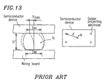
- Figure 13 illustrates representative elements among those shown above.
- the solder residue is completely removed, and the semiconductor device is connected to the wiring board by using the solder in the solder projecting electrodes alone. Therefore, the amount of solder is small. This makes it impossible to increase the height H j of the connecting portions so as to improve the reliability of the product.
- a method for producing an electronic circuit device of the present invention includes a repair step during a process of producing an electronic circuit device by aligning projecting electrodes made of brazing metal and formed on one principal plane of a semiconductor device with a substrate for mounting a semiconductor device having lands for connection corresponding to the projecting electrodes, and melting the projecting electrodes by heating, thereby mounting the semiconductor device on the substrate.
- the repair step includes, in a case where the semiconductor device once mounted is defective, removing the defective semiconductor device from the substrate and mounting a new semiconductor device on the substrate.
- the repair step includes the steps of: removing an excessive residue of a brazing metal residue remaining on the lands of the substrate from which the defective semiconductor device has been removed and leaving a uniform amount of the brazing metal residue on the lands; aligning the new semiconductor device with the substrate; and melting the brazing metal residue which is made uniform and remains on the lands and projecting electrodes of the new semiconductor device by heating, thereby connecting the new semiconductor device to the substrate.
- a method for producing an electronic circuit device of the present invention includes a repair step during a process of producing an electronic circuit device by aligning projecting electrodes made of brazing metal and formed on one principal plane of a semiconductor device with a substrate for mounting a semiconductor device having lands for connection corresponding to the projecting electrodes, and melting the projecting electrodes by heating, thereby mounting the semiconductor device on the substrate.
- the repair step includes, in a case where the semiconductor device once mounted is defective, removing the defective semiconductor device from the substrate and mounting a new semiconductor device on the substrate.
- the repair step includes the steps of: removing an excessive residue of a brazing metal residue remaining on the lands of the substrate from which the defective semiconductor device has been removed and leaving a uniform amount of the brazing metal residue on the lands; supplying brazing metal paste to tip ends of projecting electrodes of the new semiconductor device; aligning the new semiconductor device with the substrate; and melting the brazing metal residue which is made uniform and remains on the lands, projecting electrodes of the new semiconductor device, and the brazing metal paste by heating, thereby connecting the new semiconductor device to the substrate.
- the uniform amount of the brazing metal residue remaining on the lands has a height corresponding to surface tension of the brazing metal residue.
- the brazing metal residue which is made uniform and remains on the lands and the projecting electrodes of the new semiconductor device are heated to melt with light emitted by a lamp.
- a near-infrared lamp is used as the lamp.
- the step of removing an excessive residue of a brazing metal residue remaining on the lands of the substrate from which the defective semiconductor device has been removed and leaving a uniform amount of the brazing metal residue on the lands is performed by placing a plate made of solder-wettable metal over the brazing metal residue with a predetermined gap kept therebetween and heating the plate.
- the predetermined gap is about 1/4 to about 1/10 of a land diameter of the lands.
- the step of removing an excessive residue of a brazing metal residue remaining on the lands of the substrate from which the defective semiconductor device has been removed and leaving a uniform amount of the brazing metal residue on the lands is performed by a heating iron which moves at a predetermined speed while keeping in contact with the brazing metal residue.
- the heating iron is moved manually.
- the heating iron is moved manually.
- the brazing metal is eutectic solder or solder whose strength is increased by adding a slight amount of additive to eutectic solder.
- the semiconductor device is a semiconductor package having projecting electrodes in an area-array.
- the step of supplying the brazing metal paste to the tip ends of the projecting electrodes is performed by a transfer method.
- the brazing metal paste is obtained by dispersing metal powders which are the same kind as that of brazing metal in a binder.
- the projecting electrodes of the new semiconductor device and the brazing metal paste are heated to melt with light emitted by a lamp.
- a jig for making a solder residue uniform used for producing an electronic circuit device includes a plurality of pins on an outer peripheral portion of the plate.
- a groove in a shape of an expanding slot or a circular concave groove is formed in a center portion of the jig, and a depth of the groove is prescribed to be about 1/3 to about 1/2 of a height of the projecting electrodes of the semiconductor device.
- an apparatus for producing an electronic circuit device by aligning projecting electrodes made of brazing metal and formed on one principal plane of a semiconductor device with a substrate for mounting a semiconductor device having lands for connection corresponding to the projecting electrodes, and melting the projecting electrodes by heating, thereby mounting the semiconductor device on the substrate, in a case where the semiconductor device once mounted is defective, the defective semiconductor device is removed from the substrate and a new semiconductor device is mounted on the substrate.
- the apparatus includes: a holder holding the substrate; a holder holding the defective semiconductor device or the new semiconductcr device; an alignment unit aligning the substrate with the defective semiconductor device or the new semiconductor device; a unit removing an excessive residue of a brazing metal residue remaining on connecting portions of the substrate from which the defective semiconductor device has been removed and leaving a uniform amount of the brazing metal residue corresponding to surface tension of the brazing metal residue on the connecting portions; and a heating unit melting the projecting electrodes of the aligned new semiconductor device by heating, thereby connecting the new semiconductor device to the substrate.
- an apparatus for producing an electronic circuit device by aligning projecting electrodes made of brazing metal and formed on one principal plane of a semiconductor device with a substrate for mounting a semiconductor device having lands for connection corresponding to the projecting electrodes, and melting the projecting electrodes by heating, thereby mounting the semiconductor device on the substrate, in a case where the semiconductor device once mounted is defective, the defective semiconductor device is removed from the substrate and a new semiconductor device is mounted on the substrate.
- the apparatus includes: a holder holding the substrate; a holder holding the defective semiconductor device or the new semiconductor device; an alignment unit aligning the substrate with the defective semiconductor device or the new semiconductor device; a unit removing an excessive residue of a brazing metal residue remaining on connecting portions of the substrate from which the defective semiconductor device has been removed and leaving a uniform amount of the brazing metal residue corresponding to surface tension of the brazing metal residue on the connecting portions; a jig for transferring brazing metal paste to tip ends of the projecting electrodes of the new semiconductor device, a groove in a shape of an expanding slot or a circular concave groove being formed in a center portion of the jig, and a depth of the groove being prescribed to be about 1/3 to about 1/2 of a height of the projecting electrodes of the semiconductor device; and a heating unit melting the projecting electrodes of the aligned new semiconductor device by heating, thereby connecting the new semiconductor device to the substrate.
- the unit removing an excessive residue of a brazing metal residue remaining on connecting portions of the substrate from which the defective semiconductor device has been removed and leaving a uniform amount of the brazing metal residue on the connecting portions is a heating iron which moves at a predetermined speed while keeping in contact with the brazing metal residue or a jig for making a solder residue uniform including a plurality of pins on an outer peripheral portion.
- the heating unit is a near-infrared lamp.
- the transfer step as described above is not required.
- the height of the printed solder i.e., height of the solder residue after being shaped
- the solder residue remaining on a wiring board from which a defective semiconductor device has been removed is left on purpose, instead of being completely removed, whereby a sufficient amount of solder is secured.
- the solder residue remaining on the wiring board from which the defective semiconductor device has been removed is left in a nonuniform amount.
- the solder residue can be controlled to a uniform amount and a uniform height. This control can be easily performed by heating the solder residue by using the above-mentioned jig for making the solder residue uniform.
- a uniform amount of solder paste can be easily supplied to a semiconductor device, which is convenient. More specifically, the use of the above-mentioned jig for transferring brazing metal paste facilitates the transfer of solder paste.
- solder paste in order to increase the height of the connecting portions, solder paste should be transferred as much as possible. Considering the relationship between the amount of the solder residue remaining on the wiring board and the surface tension thereof, the transfer amount is preferably about 1/3 or more of the height of the solder projecting electrodes. If too great an amount of solder paste is transferred, as shown in Figure 3A (described later), solder paste 12 may adhere to a semiconductor device 20 to form a bridge 23 between solder projecting electrodes 21 . When such a bridge 23 is formed, as shown in Figure 3B , the bridge 23 reflows together with the solder projecting electrodes 21 when the semiconductor device 20 is mounted and heated.
- the transfer amount should be limited to about 1/2 of the height of the solder projecting electrodes 21 , i.e., a value not exceeding an equator surface of the solder projecting electrodes 21 .
- the depth of the groove of the jig for transferring brazing metal paste is prescribed to be about 1/2 to about 1/3 of the height of the solder projecting electrodes, whereby the transfer amount is prescribed to be about 1/2 to about 1/3 of the height of the solder projecting electrodes 21 .
- a heating device for re-connecting a new semiconductor device to a wiring board should not involve an excessive external force. More specifically, without an excessive external force, a semiconductor device and a wiring board which have been aligned with each other will not be shifted in position. Thus, the repair step can be more easily and efficiently performed. Because of this, according to the present invention, a lamp which does not involve an external force is used. As the lamp, a near-infrared lamp (IR lamp) is preferably used for the following reason.
- Si is used as a material mainly for a circuit board. Si transmits light in a near-infrared region (wavelength: about 1 to about 5 ⁇ m).
- the light with a wavelength of about 1 to about 5 ⁇ m passes through Si to directly and efficiently heat the solder projecting electrodes and solder paste.
- an IR lamp capable of emitting light with a wavelength of about 1 to about 5 ⁇ m is preferably used.
- eutectic solder or eutectic solder with a slight amount of additive added thereto as brazing metal can improve solder strength.
- the invention described herein makes possible the advantages of: (1) providing a method for producing an electronic circuit device which is capable of securing the amount of solder sufficient for connecting a semiconductor device to a wiring board, thereby increasing the height of the connecting portions to improve the reliability of a product; (2) providing a jig for making a solder residue uniform and a jig for transferring a brazing metal paste used in the production method; and (3) providing an apparatus for producing an electronic circuit device used for performing the production method.
- Figure 1 is a flow chart showing a repair process in a method for producing an electronic circuit device according to the present invention.
- Figure 2A is a perspective view showing a jig for transferring solder paste used for performing the method according to the present invention
- Figure 2B is a perspective view showing a state in which the jig is filled with transfer paste.
- FIGS 3A and 3B illustrate inconvenience in the case where the amount of transfer paste is excessive.
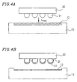
- Figures 4A and 4B show steps of transferring solder paste.
- Figure 5A is a perspective view showing another jig for transferring solder paste used for performing the method according to the present invention
- Figure 5B is a perspective view showing a state in which the jig is filled with transfer paste.
- Figure 6 is a perspective view showing a jig for making a solder residue uniform.
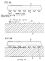
- Figures 7A through 7C show steps of making a solder residue on a wiring board uniform using the jig shown in Figure 6 .
- Figures 8A through 8C show steps of making a solder residue uniform using another jig for making a solder residue uniform.
- Figures 9A and 9B respectively show a semiconductor device and a wiring board to which the present invention is applied.
- Figure 10 is a graph illustrating a range of a land diameter of a wiring board to which the present is applied.
- Figure 11 is a perspective view of an apparatus for producing an electronic circuit device according to the present invention.
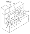
- Figure 12 is a perspective view of another apparatus for producing an electronic circuit device according to the present invention.
- Figure 13 illustrates the Coffin ⁇ Manson connection fatigue life expression.
- Figures 1 through 7 show a method for producing an electronic circuit device in Embodiment 1 according to the present invention.
- the method according to the present invention is characterized by a repair step which will be outlined with reference to Figure 1 .
- Step S1 it is confirmed that a semiconductor device on a wiring board is defective.
- the defective semiconductor device is heated by a lamp so as to melt solder projecting electrodes, whereby the semiconductor device is removed from the wiring board.
- Step S3 after the defective semiconductor device is removed, an excessive solder residue remaining on the wiring board is removed so that only a uniform amount thereof is left.
- Step S4 a new semiconductor device is prepared.
- solder paste is provided by a transfer method to tip ends of solder projecting electrodes of the device, whereby the device is ready to be mounted.
- Step S6 the new semiconductor device to which the solder paste has been transferred is aligned with the wiring board on which a uniform amount of solder residue remains.
- Step S7 the new semiconductor device which has been mounted on the wiring board is heated by a lamp, whereby the solder projecting electrodes and the solder paste melt. Thus, the semiconductor device is connected to the wiring board.
- Step S8 the repair is completed.
- a near-infrared lamp is preferably used for the following reason.
- Si As a material of choice for wiring boards, Si is used. Si transmits light in a near-infrared region (wavelength: about 1 to about 5 ⁇ m). When the light with a wavelength of about 1 to about 5 ⁇ m is used, the light passes through Si to directly heat the solder projecting electrodes and solder paste with efficiency. Thus, the IR lamp which emits light with a wavelength of about 1 to about 5 ⁇ m is preferable.
- the step of transferring solder paste at Step 5 is performed, for example, by using a solder paste transfer jig 10 shown in Figure 2 .
- the jig 10 is a rectangular solid which has a groove 11 in the shape of an expanding slot at a center portion of its surface.
- the groove 11 is provided for the purpose of allowing solder paste 12 to have constant thickness. It is appropriate that the depth of the groove 11 is about 1/2 to about 1/3 of the height of solder projecting electrodes 21 of a semiconductor device 20 (see Figure 3 ) for the following reason.
- the solder paste 12 may be transferred as much as possible.
- the depth of the groove 11 is preferably at least about 1/3 of the height of the solder projecting electrodes 21 .
- the transfer amount is excessive, there is a possibility that the solder paste 12 may adhere to a semiconductor device 20 to form a bridge 23 between the solder projecting electrodes 21 , as shown in Figure 3A .
- the bridge 23 reflows together with the solder projecting electrodes 21 when the semiconductor device 20 is mounted and heated.
- the transfer amount should be set at about 1/2 of the height of the solder projecting electrodes 21 , i.e., at a value not exceeding an equator surface of the solder projecting electrodes 21 .
- the depth of the groove 11 of the jig 10 is set to be about 1/2 to about 1/3 of the height of the solder projecting electrodes 21 , whereby the transfer amount is set to be about 1/2 to about 1/3 of the height of the solder projecting electrodes 21 .
- the solder paste 12 is put in the groove 11 of the jig 10 , and the surface of the solder paste 12 is flattened out by a squeegee or the like (not shown) so that the groove 11 is filled with the solder paste 12 .
- the semiconductor device 20 is pressed against the jig 10 (see Figure 4A ), whereby the solder paste 12 is allowed to adhere to the tip ends of the solder projecting electrodes 21 .
- the semiconductor device 20 is lifted up.
- the step of transferring the solder paste 12 is completed (see Figure 4B ).
- FIGS 5A and 5B show another example of a solder paste transfer jig.
- a jig 10' is in the shape of a disk which has a circular groove 11' in a center portion.
- a projection 13 whose surface is as high as the surface of the jig 10' is disposed in a center portion of the circular groove 11' .
- the depth of the groove 11' is set to be about 1/2 to about 1/3 of the height of the solder projecting electrodes 21 in the same way as the above.
- FIG 6 shows a jig for making the amount of the solder residue on the wiring board uniform at Step 3.
- a jig 40 is composed of a solder-wettable metal plate 41 in the shape of a rectangular solid provided with pins 42 at four corners.
- the pins 42 have the function of keeping a constant gap with respect to a wiring board 30 (see Figure 7 ).
- solder residue spreading over the metal plate 41 is not shown. Due to the surface tension of the solder, the solder stops spreading over the jig 40 , with a predetermined amount of solder remaining on lands 33 for connection of the wiring board 30 . At this time, if required, a flux or the like may be coated on the jig 40 or the wiring board 30 . Thereafter, the jig 40 is removed, and,a uniform amount of solder 32 remains on the lands 33 of the wiring board 30 (see Figure 7C ).
- the height of the pins 42 is important. It has been confirmed that the height of the pins 42 is preferably about 1/4 to about 1/10 of the diameter of the lands 33 .
- a semiconductor package having solder projecting electrodes in an area array is used as a semiconductor device to which the present invention is applied.
- FIGS 8A through 8C show a method for producing an electronic circuit device in Embodiment 2 according to the present invention.
- Embodiment 2 is characterized by a method for making a solder residue uniform during a repair step.
- the solder residue is made uniform by using a soldering iron. The step of making the solder residue uniform will be described in detail.
- a soldering iron 50 is positioned above a wiring board 30 . More specifically, the soldering iron 50 is positioned at such a height that its tip end can come into contact with the solder residue 31 .
- the heated soldering iron 50 is moved in the horizontal direction at a constant speed.
- the soldering iron 50 is desirably coated with a flux.
- soldering iron 50 When the soldering iron 50 is moved, the solder residue 31 is heated by the soldering iron 50 to melt, thereby spreading over the soldering iron 50 and lands 33 .
- the solder spreading over the soldering iron 50 is not shown. However, due to the surface tension of the solder, the solder stops spreading with a predetermined amount of solder remaining on the lands 33 of the wiring board 30 (see Figure 8C ). It was confirmed that the soldering iron 50 is preferably moved at such a speed as to pass by the lands 33 at about 1/10 to about 1 second.
- soldering iron 50 is manually moved in the present embodiment, it may be automatically moved by an apparatus (described later) according to the present invention .
- solder residue 31 is scraped by manually moving the soldering iron 50 to be shaped, it is required to consider a land diameter L D . More specifically, depending upon the size of the land diameter L D of the wiring board 30 , such a shaping method causes variation or the like of the solder residue 31 , resulting in an undesirable state. A preferable range of the land diameter L D will be described below.
- solder projecting electrode size H D of a semiconductor device 20 a solder projecting electrode pitch H P thereof, and a land pitch L P of a wiring board 30 (same as the solder projecting electrode pitch H P ) will be described.
- the solder projecting electrode size H D is about 0.2 mm ⁇ to about 0.8 mm ⁇ , and the solder projecting electrode pitch H P and the land pitch L P of the wiring board 30 are respectively about 0.5 mm to about 1.27 mm.
- the preferable height of the solder residue after being shaped varies depending upon the land diameter L D (for example, as shown in Figure 10 , the preferable height of the solder residue in the case of the land diameter L D of about 150 ⁇ m ⁇ is about 55 ⁇ m to about 90 ⁇ m; and the preferable height of the solder residue in the case of the land diameter L D of about 250 ⁇ m ⁇ is about 60 ⁇ m to about 100 ⁇ m).
- the preferable land diameter L D was confirmed to be in the range of about 150 ⁇ m ⁇ to about 550 ⁇ m ⁇ .
- the wiring board 30 having a land diameter L D of about 800 ⁇ m ⁇ or more, it is not preferable to shape the solder residue 31 by scraping it with a soldering iron. It was confirmed that dispensing solder paste is preferable in this case.
- the land diameter L D exceeds about 1 mm ⁇ , the minimum value of the distribution of the solder residue 31 tends to decrease and the variation thereof tends to increase. Thus, it was confirmed that the land diameter exceeding about 1 mm ⁇ is not preferable.
- Embodiment 1 adopts a process for transferring solder paste to the solder projecting electrodes 21 of the new semiconductor device 20 , thereby increasing the height of the connecting portions.
- a transfer step is not required. More specifically, a repair method omitting Step S5 (transfer step) in Embodiment 1 can be performed.
- the height of the printed solder i.e., height of the solder residue after being shaped
- the height of the printed solder is about 70 ⁇ m ⁇ . Therefore, as is understood from Figure 10 , it was confirmed that a reliable repair step can be performed even without performing Step S5.
- Table 1 shows a test result of temperature cycle reliability evaluation of a semiconductor device repaired in accordance with the method of the present invention and of a semiconductor device which is not defective.
- the land pitch of the semiconductor device used herein was 0.6 mm. It was confirmed that the repaired semiconductor device has the same reliability as that of the device which is not defective.
- Table 2 shows a comparison result of the occurrence of disconnection in a semiconductor device which has been repaired in accordance with the present invention and a semiconductor device which has been repaired by the conventional repair method (i.e., a semiconductor device which has been repaired by completely removing a solder residue without transferring solder paste).
- the land pitch of the semiconductor device used herein was 0.8 mm.
- the wiring board 30 including the lands with a land diameter L D of about 0.3 mm ⁇ was used.
- the lands were coated with about 2 to about 3 ⁇ m of electroless Ni plating and flush Au plating.
- IR lamp a near-infrared lamp with a power of 225 watts made of tungsten filaments produced by Phoenix Elect. was used. Light emitted by the IR lamp was condensed by a parabolic mirror so as to have a focal point in the vicinity of the surface of the wiring board and the semiconductor device. The semiconductor device was heated to 250°C by the IR lamp in about one minute.
- Solder paste (RMA501-88-3-30, produced by Alphametals Co., Ltd.) having a viscosity of 300,000 centipoises (cP) was used in the experiment, which was obtained by kneading minute solder powders (average size: 30 ⁇ m) of eutectic solder (Sn 63% and Pb 37%) with a RMA type flux.
- solder paste was placed in the jig 10 shown in Figures 2A and 2B which was obtained by forming a groove with a depth of about 150 ⁇ m in an SUS 301 plate (thickness: about 6 mm) by milling.
- the solder paste was squeegeed with a glass plate (7027, produced by Corning) having a thickness of about 1.1 mm so as to be flattened in the groove.
- the semiconductor device 20 was attached to a vacuum pincette (392, produced by Hakko Kinzoku Co., Ltd.). The semiconductor device 20 was manually pressed against the solder paste flattened to a thickness of about 50 ⁇ m. The semiconductor device 20 was allowed to stand for at least 2 minutes so as to be intimately contacted by the solder paste.
- the solder residue was removed by using the jig 40 in which four female threads (ISO ⁇ M2 threads) are provided on a brass plate (thickness: about 1.0 mm) so as to allow tip ends thereof to project from the brass plate by about 0.1 mm to form pins 42 (see Figure 6 ).
- the brass plate was thinly soldered by a dip soldering method.
- the soldered brass plate was further coated with a flux (RF-350-RMA, produced by Nihon Alumit Co., Ltd.) by a brush.
- the jig 40 was placed over the solder residue and heated by the IR lamp at about 1225 watts/min.
- the solder residue assumed a shape of a hill such as shown in Figures 7C and 8C with a thickness of about 50 to about 70 ⁇ m.
- a flux (RF-350-RMA) was coated onto the solder residue by a brush, and the solder residue was rubbed with a soldering iron (926M, produced by Hakko Kinzoku Co., Ltd.) having an iron tip (900M-TI-C) at 300°C to 320°C.
- a soldering iron (926M, produced by Hakko Kinzoku Co., Ltd.) having an iron tip (900M-TI-C) at 300°C to 320°C.
- the solder residue similar to the above was also obtained.
- the semiconductor device 20 to which the solder paste has been transferred was attached to a vacuum pincette and placed on the wiring board 30 by visual alignment marks.
- the semiconductor device 20 placed on the wiring board 30 was heated by the IR lamp so as to allow the solder residue, the solder projecting electrodes 21 and the transferred solder paste to melt.
- the semiconductor device 20 was connected to the wiring board 30 .
- the solder melts it returns to a normal position due to the surface tension even if it is displaced (self-alignment effect). Therefore, in the case of lands with a diameter of about 0.3 mm, the lands can be adjusted by up to about ⁇ 0.15 mm. Because of this, it was confirmed that the semiconductor device 20 was able to be mounted on the wiring board 30 by visual alignment.
- Figure 11 shows an apparatus for producing an electronic circuit device in Embodiment 4 according to the present invention.
- the apparatus includes a substrate stage 130 which holds a wiring board 30 and is capable of precisely moving for alignment, a solder paste transfer jig 10 , a heating lamp 160 (IR lamp) for removing a defective semiconductor device 20' , making a solder residue uniform, and mounting a new semiconductor device 20 , a pickup tool 170 for holding and moving the semiconductor device 20 , an optical system 190 for alignment, and a monitor TV 191 for confirming alignment.
- a substrate stage 130 which holds a wiring board 30 and is capable of precisely moving for alignment
- a solder paste transfer jig 10 a heating lamp 160 (IR lamp) for removing a defective semiconductor device 20' , making a solder residue uniform, and mounting a new semiconductor device 20
- a pickup tool 170 for holding and moving the semiconductor device 20
- an optical system 190 for alignment
- a monitor TV 191 for confirming alignment.
- the pickup tool 170 , the heating lamp 160 , and the optical system 190 for alignment can be moved horizontally. They can be moved, for example, by a linear motor (not shown).
- the lamp 160 is moved onto the defective semiconductor device 20' .
- the lamp 160 is lit up to heat the defective semiconductor device 20' .
- the solder of the connecting portions is heated to melt, which enables the defective semiconductor device 20' to be removed.
- the pickup tool 170 is moved to be positioned above the defective semiconductor device 20' and attaches to it, whereby the defective semiconductor device 20' is removed.
- the above-mentioned jig 40 is placed over the solder residue 31 remaining on the wiring board 30 and heated by the lamp 160 , whereby the solder residue is made uniform.
- the new semiconductor device 20 is attached to the pickup tool 170 .
- solder paste 12 is placed in the groove 11 of the solder paste transfer jig 10 and flattened with a squeegee or the like.
- the semiconductor device 20 attached to the pickup tool 170 is pressed against the groove 11 of the solder paste transfer jig 10 filled with the solder paste 12 , whereby the solder paste 12 is transferred to tip ends of the solder projecting electrodes 21 of the semiconductor device 20 .
- the pickup tool 170 is moved to be positioned above the wiring board 30 , attaching to the semiconductor device 20 .
- the substrate stage 130 is moved so as to align the wiring board 30 with the semiconductor device 20 , whereby the semiconductor device 20 is mounted on the wiring board 30 .
- the semiconductor device 20 is heated by the lamp 160 , thereby heating and melting the solder to connect the semiconductor device 20 with the wiring board 30 .
- Figure 12 shows an apparatus for producing an electronic circuit device in Embodiment 5 according to the present invention.
- This apparatus is different from that in Embodiment 4 only in that a soldering iron 50 and a movement mechanism 51 for horizontally moving the soldering iron 50 are provided. Therefore, like reference numerals refer to like parts. The description of the parts which have been described in Embodiment 4 will be omitted here.
- the movement mechanism 51 is operated, for example, by a linear motor.
- the lamp 160 is moved to be positioned above the defective semiconductor device 20' and heats it, whereby the solder of the connecting portions is heated to melt.
- the pickup tool 170 is moved to be positioned above the defective semiconductor device 20' and attaches to it, whereby the defective semiconductor device 20' is removed.
- a soldering iron 50 is brought into contact with the wiring board 30 .
- the movement mechanism 51 is operated under this condition, whereby the solder residue 31 on the wiring board 30 is made uniform.
- the new semiconductor device 20 is attached to the pickup tool 170 .
- the semiconductor device 20 is pressed against the groove 11 of the solder paste transfer jig 10 filled with solder paste 12 .
- the solder paste 12 is transferred to tip ends of the solder projecting electrodes 21 of the semiconductor device 20 .
- the wiring board 30 is aligned with the semiconductor device 20 , whereby the semiconductor device 20 is mounted on the wiring board 30 . Then, the semiconductor device 20 is heated with the lamp 160 so as to be connected with the wiring board 30 .
- the apparatus in Embodiment 5 it is critical that the movement mechanism 51 of the soldering iron 50 is in contact with the soldering iron 50 . However, since the margin of the movement speed is large, the soldering iron 50 may be manually moved without using the movement mechanism 51 . In this case, the apparatus may have the same structure as that in Embodiment 4.
- solder residue is left on a wiring board in accordance with the surface tension thereof, and a new semiconductor device is provided with solder paste. Therefore, a sufficient amount of solder can be secured for a repaired semiconductor device.
- this increases the height H j of the connecting portions and decreases the maximum strain ⁇ max in the connecting portions, so that a connection failure (i.e., disconnection) does not occur.
- a connection failure i.e., disconnection
- the transfer step as described above is not required.
- the solder residue remaining on the wiring board from which a defective semiconductor device has been removed is left on purpose, instead of being completely removed, whereby a sufficient amount of solder is secured.
- the solder residue remaining on the wiring board from which the defective semiconductor device has been removed is left in a nonuniform amount.
- the solder residue can be controlled to a uniform amount and a uniform height. This control can be easily performed by heating the solder residue, using the jig for making the solder residue uniform according to the present invention.
- a uniform amount of solder paste can be easily supplied to the semiconductor device, which is convenient. More specifically, the use of the above-mentioned jig for transferring brazing metal paste facilitates the transfer of solder paste.
- solder paste in order to increase the height of the connecting portions, solder paste should be transferred as much as possible. Considering the relationship between the amount of the solder residue remaining on the wiring board and the surface tension thereof, the transfer amount is preferably about 1/3 or more of the height of the solder projecting electrodes. If too much amount of solder paste is transferred, a bridge may be formed between the solder projecting electrodes. When such a bridge is formed, the molten solder is integrated due to the surface tension thereof to form a solder projecting electrode having a large diameter. In order to prevent such a solder projecting electrode from being formed, the transfer amount should be limited to about 1/2 of the height of the solder projecting electrodes, i.e., a value not exceeding an equator surface of the solder projecting electrodes.
- the depth of the groove of the jig for transferring brazing metal paste is prescribed to be about 1/2 to about 1/3 of the height of the solder projecting electrodes, whereby the transfer amount is prescribed to be about 1/2 to about 1/3 of the height of the solder projecting electrodes.
- a heating device for re-connecting a new semiconductor device to the wiring board should not involve any excessive external force. More specifically, without an excessive external force, the semiconductor device and the wiring board which have been aligned with each other will not be shifted in position. Thus, the repair step can be more easily and efficiently performed. Because of this, according to the present invention, a lamp which does not involve an external force is used. As the lamp, a near-infrared lamp (IR lamp) is preferably used for the following reason.
- Si is used as a material of choice for a circuit board. Si transmits light in a near-infrared region (wavelength: about 1 to about 5 ⁇ m).
- the IR lamp which is capable of emitting light with a wavelength of about 1 to about 5 ⁇ m is preferably used.
- eutectic solder or eutectic solder with a slight amount of additive added thereto as brazing metal can improve solder strength.
Landscapes
- Engineering & Computer Science (AREA)
- Manufacturing & Machinery (AREA)
- Microelectronics & Electronic Packaging (AREA)
- Electric Connection Of Electric Components To Printed Circuits (AREA)
- Wire Bonding (AREA)
Applications Claiming Priority (3)
| Application Number | Priority Date | Filing Date | Title |
|---|---|---|---|
| JP316555/96 | 1996-11-27 | ||
| JP31655596A JP3279940B2 (ja) | 1996-11-27 | 1996-11-27 | 電子回路装置の製造方法、半田残渣均一化治具、金属ロウペースト転写用治具及び電子回路装置の製造装置 |
| JP31655596 | 1996-11-27 |
Publications (3)
| Publication Number | Publication Date |
|---|---|
| EP0845807A2 true EP0845807A2 (de) | 1998-06-03 |
| EP0845807A3 EP0845807A3 (de) | 1999-04-07 |
| EP0845807B1 EP0845807B1 (de) | 2003-01-29 |
Family
ID=18078410
Family Applications (1)
| Application Number | Title | Priority Date | Filing Date |
|---|---|---|---|
| EP97120112A Expired - Lifetime EP0845807B1 (de) | 1996-11-27 | 1997-11-17 | Verfahren und Vorrichtung zur Herstellung einer elektronischen Schaltungsanordnung mit gleichförmigen Lötrückständen bei Übertragung von Lotpaste |
Country Status (7)
| Country | Link |
|---|---|
| US (1) | US6062460A (de) |
| EP (1) | EP0845807B1 (de) |
| JP (1) | JP3279940B2 (de) |
| KR (1) | KR100279133B1 (de) |
| CN (1) | CN1101642C (de) |
| DE (1) | DE69718755T2 (de) |
| TW (1) | TW422752B (de) |
Cited By (2)
| Publication number | Priority date | Publication date | Assignee | Title |
|---|---|---|---|---|
| WO2007023825A1 (en) * | 2005-08-25 | 2007-03-01 | Matsushita Electric Industrial Co., Ltd. | Electronic component mounting method |
| WO2012136733A1 (en) * | 2011-04-08 | 2012-10-11 | Micronic Mydata AB | Method and fluid transfer unit having squeegees for providing a smooth surface of fluid |
Families Citing this family (20)
| Publication number | Priority date | Publication date | Assignee | Title |
|---|---|---|---|---|
| JP3239335B2 (ja) | 1999-08-18 | 2001-12-17 | インターナショナル・ビジネス・マシーンズ・コーポレーション | 電気的接続用構造体の形成方法およびはんだ転写用基板 |
| JP3334693B2 (ja) * | 1999-10-08 | 2002-10-15 | 日本電気株式会社 | 半導体装置の製造方法 |
| AU5876501A (en) * | 2000-05-17 | 2001-11-26 | Hitachi Chemical Co. Ltd. | Method for repairing circuit connecton part, and structure and method for connecting circuit terminal of circuit repaired by the method |
| US6509318B1 (en) * | 2000-09-29 | 2003-01-21 | The Regents Of The University Of California | TGF-B inhibitors and methods |
| US20030019576A1 (en) * | 2001-06-27 | 2003-01-30 | Loctite Corporation | Electronic component removal method through application of infrared radiation |
| US6637641B1 (en) * | 2002-05-06 | 2003-10-28 | Emc Corporation | Systems and methods for manufacturing a circuit board |
| US6910615B2 (en) * | 2003-03-27 | 2005-06-28 | International Business Machines Corporation | Solder reflow type electrical apparatus packaging having integrated circuit and discrete components |
| KR100542552B1 (ko) | 2003-08-21 | 2006-01-11 | 삼성전자주식회사 | 인쇄회로기판, 및 이 인쇄회로기판을 갖는 화상기록장치 |
| JP4799997B2 (ja) * | 2005-10-25 | 2011-10-26 | 富士通株式会社 | 電子機器用プリント板の製造方法およびこれを用いた電子機器 |
| KR100807478B1 (ko) | 2007-03-06 | 2008-02-25 | 삼성전기주식회사 | 솔더 형성 방법 및 솔더 형성용 캡 |
| US8371497B2 (en) * | 2009-06-11 | 2013-02-12 | Qualcomm Incorporated | Method for manufacturing tight pitch, flip chip integrated circuit packages |
| CN101609793B (zh) * | 2009-06-30 | 2011-07-27 | 中国航空工业集团公司洛阳电光设备研究所 | Bga器件漏印工装及印制板bga器件的更新焊接方法 |
| JP5726581B2 (ja) * | 2011-03-16 | 2015-06-03 | 富士機械製造株式会社 | 電子部品リペア機および生産ライン |
| JP2015220353A (ja) * | 2014-05-19 | 2015-12-07 | 富士通株式会社 | 電子部品の取り付け方法及びハンダペーストの転写方法並びに電子部品の取り付け装置 |
| WO2016022755A2 (en) | 2014-08-06 | 2016-02-11 | Greene Lyon Group, Inc. | Rotational removal of electronic chips and other components from printed wire boards using liquid heat media |
| US10269762B2 (en) * | 2015-10-29 | 2019-04-23 | Taiwan Semiconductor Manufacturing Company, Ltd. | Rework process and tool design for semiconductor package |
| KR20190130148A (ko) * | 2017-05-12 | 2019-11-21 | 헤레우스 도이칠란트 게엠베하 운트 코. 카게 | 금속 페이스트에 의해 부품들을 연결하기 위한 방법 |
| FR3066937B1 (fr) | 2017-05-30 | 2019-07-12 | Continental Automotive France | Dispositif de chauffe |
| TWI632666B (zh) * | 2017-12-11 | 2018-08-11 | Asti Global Inc., Taiwan | 半導體晶片修補方法以及半導體晶片修補裝置 |
| CN115295428A (zh) * | 2022-07-04 | 2022-11-04 | 广州市鸿利显示电子有限公司 | 一种利用报废基板进行芯片贴装方法及发光板 |
Family Cites Families (26)
| Publication number | Priority date | Publication date | Assignee | Title |
|---|---|---|---|---|
| US3804667A (en) * | 1969-09-30 | 1974-04-16 | Techni Tool Inc | Method for opening eyelet holes in printed circuit boards |
| US3731866A (en) * | 1971-01-04 | 1973-05-08 | Cogar Corp | Apparatus for removing and replacing multi-pinned components mounted on circuit boards |
| US4136444A (en) * | 1977-06-06 | 1979-01-30 | Burroughs Corporation | Semiautomatic solid chip removal apparatus |
| JPS54143871A (en) * | 1978-04-28 | 1979-11-09 | Kokusan Denki Co | Method of producing hybrid ic circuit |
| US4436242A (en) * | 1981-12-15 | 1984-03-13 | Rca Corporation | Desoldering tool and method of desoldering leadless components |
| US4441647A (en) * | 1982-06-04 | 1984-04-10 | Northern Telecom Limited | Resoldering tool for ceramic substrate hybrid electronic circuits |
| US4444559A (en) * | 1982-06-28 | 1984-04-24 | International Business Machines Corporation | Process and apparatus for unsoldering solder bonded semiconductor devices |
| US4771932A (en) * | 1985-12-09 | 1988-09-20 | Henry Kim | Method for soldering and desoldering electronic components |
| US4878611A (en) * | 1986-05-30 | 1989-11-07 | American Telephone And Telegraph Company, At&T Bell Laboratories | Process for controlling solder joint geometry when surface mounting a leadless integrated circuit package on a substrate |
| ES2002897A6 (es) * | 1986-11-04 | 1988-10-01 | Del Pino Millan Bienvenido | Desoldador automatico portatil |
| ATE91064T1 (de) * | 1987-08-31 | 1993-07-15 | Siemens Ag | Loetkopf zum ein- und ausloeten von bauelementen. |
| JPH01209736A (ja) * | 1988-02-17 | 1989-08-23 | Nec Corp | 半導体素子の交換方法 |
| US5154793A (en) * | 1988-09-27 | 1992-10-13 | General Electric Company | Method and apparatus for removing components bonded to a substrate |
| US5072874A (en) * | 1991-01-31 | 1991-12-17 | Microelectronics And Computer Technology Corporation | Method and apparatus for using desoldering material |
| GB2259039A (en) * | 1991-09-02 | 1993-03-03 | Pdr Microelectronics Limited | Directed infra-red rework station |
| JP2813507B2 (ja) * | 1992-04-23 | 1998-10-22 | 三菱電機株式会社 | ボンディング方法およびボンディング装置 |
| US5311404A (en) * | 1992-06-30 | 1994-05-10 | Hughes Aircraft Company | Electrical interconnection substrate with both wire bond and solder contacts |
| JPH0618433A (ja) * | 1992-06-30 | 1994-01-25 | Mitsubishi Electric Corp | ボンディング装置及び方法 |
| JP2714520B2 (ja) * | 1992-08-28 | 1998-02-16 | 株式会社日立製作所 | 実装部品着脱装置 |
| US5325582A (en) * | 1992-10-19 | 1994-07-05 | Trw Inc. | Multi-function workstation for assembly and repair of printed wiring board assemblies |
| US5439162A (en) * | 1993-06-28 | 1995-08-08 | Motorola, Inc. | Direct chip attachment structure and method |
| JP3173547B2 (ja) * | 1994-03-18 | 2001-06-04 | 松下電器産業株式会社 | 半田バンプの形成方法 |
| US5783025A (en) * | 1994-06-07 | 1998-07-21 | Texas Instruments Incorporated | Optical diebonding for semiconductor devices |
| JPH0846351A (ja) * | 1994-08-01 | 1996-02-16 | M & M Prod Kk | プリント回路基板からのbgaパッケージの取り外し方法、及び実装方法と、これに使用するノズル |
| US5603857A (en) * | 1995-02-24 | 1997-02-18 | Assembly Technologies International, Inc. | Handheld electric heater for removing or replacing surface-mounted integrated circuits from a circuit board |
| US5758817A (en) * | 1996-03-19 | 1998-06-02 | Resource Concepts, Inc. | Apparatus and process for removing surface mounted components from printed wiring assemblies |
-
1996
- 1996-11-27 JP JP31655596A patent/JP3279940B2/ja not_active Expired - Fee Related
-
1997
- 1997-11-14 TW TW086116999A patent/TW422752B/zh not_active IP Right Cessation
- 1997-11-17 US US08/971,985 patent/US6062460A/en not_active Expired - Fee Related
- 1997-11-17 DE DE69718755T patent/DE69718755T2/de not_active Expired - Fee Related
- 1997-11-17 EP EP97120112A patent/EP0845807B1/de not_active Expired - Lifetime
- 1997-11-26 KR KR1019970062990A patent/KR100279133B1/ko not_active Expired - Fee Related
- 1997-11-27 CN CN97126212A patent/CN1101642C/zh not_active Expired - Fee Related
Cited By (2)
| Publication number | Priority date | Publication date | Assignee | Title |
|---|---|---|---|---|
| WO2007023825A1 (en) * | 2005-08-25 | 2007-03-01 | Matsushita Electric Industrial Co., Ltd. | Electronic component mounting method |
| WO2012136733A1 (en) * | 2011-04-08 | 2012-10-11 | Micronic Mydata AB | Method and fluid transfer unit having squeegees for providing a smooth surface of fluid |
Also Published As
| Publication number | Publication date |
|---|---|
| KR100279133B1 (ko) | 2001-02-01 |
| US6062460A (en) | 2000-05-16 |
| DE69718755T2 (de) | 2004-01-08 |
| CN1101642C (zh) | 2003-02-12 |
| DE69718755D1 (de) | 2003-03-06 |
| CN1183706A (zh) | 1998-06-03 |
| TW422752B (en) | 2001-02-21 |
| JP3279940B2 (ja) | 2002-04-30 |
| KR19980042767A (ko) | 1998-08-17 |
| EP0845807B1 (de) | 2003-01-29 |
| JPH10163624A (ja) | 1998-06-19 |
| EP0845807A3 (de) | 1999-04-07 |
Similar Documents
| Publication | Publication Date | Title |
|---|---|---|
| US6062460A (en) | Apparatus for producing an electronic circuit | |
| EP1386356B1 (de) | Flussmittelfreie flip-chip-verbindung | |
| JPH06103703B2 (ja) | 半田付け方法 | |
| US5973406A (en) | Electronic device bonding method and electronic circuit apparatus | |
| JP3266414B2 (ja) | はんだ供給法 | |
| JP2510688B2 (ja) | 過剰はんだ除去装置 | |
| KR100982183B1 (ko) | 납땜 실장 구조의 제조 방법 | |
| JP3385943B2 (ja) | 金バンプ付電子部品の実装方法 | |
| JP2002057453A (ja) | 半導体装置のリペア方法 | |
| JP3544439B2 (ja) | 接続ピンと基板実装方法 | |
| JPH0983128A (ja) | 半導体モジュールの接合構造 | |
| JP5328288B2 (ja) | 半導体装置のはんだ付け方法及び実装構造 | |
| JP2000244110A (ja) | Bgaパッケージの実装方法 | |
| CN120282612A (zh) | Mini-LED显示屏模块及其制备方法、Mini-LED显示屏 | |
| JPH07202401A (ja) | 金属バンプの供給方法及びその装置 | |
| JPS63128574A (ja) | コネクタピン | |
| JPH0774209A (ja) | 半導体装置の製造方法 | |
| JPH08162482A (ja) | 半導体装置 | |
| JPH0613744A (ja) | 電子部品接合方法 | |
| JPH08153964A (ja) | 半田付け方法 | |
| JP2000349184A (ja) | 電子装置及びその製造方法 | |
| JPH03233951A (ja) | 半導体素子の電極接続方法 | |
| JPH0964529A (ja) | Bgaパッケージの実装方法 | |
| JPH06283568A (ja) | ツール加熱半田付方法 | |
| JPS63313662A (ja) | 熱圧着ヘッド |
Legal Events
| Date | Code | Title | Description |
|---|---|---|---|
| PUAI | Public reference made under article 153(3) epc to a published international application that has entered the european phase |
Free format text: ORIGINAL CODE: 0009012 |
|
| AK | Designated contracting states |
Kind code of ref document: A2 Designated state(s): DE FR GB |
|
| AX | Request for extension of the european patent |
Free format text: AL;LT;LV;MK;RO;SI |
|
| PUAL | Search report despatched |
Free format text: ORIGINAL CODE: 0009013 |
|
| AK | Designated contracting states |
Kind code of ref document: A3 Designated state(s): AT BE CH DE DK ES FI FR GB GR IE IT LI LU MC NL PT SE |
|
| AX | Request for extension of the european patent |
Free format text: AL;LT;LV;MK;RO;SI |
|
| 17P | Request for examination filed |
Effective date: 19991005 |
|
| AKX | Designation fees paid |
Free format text: DE FR GB |
|
| 17Q | First examination report despatched |
Effective date: 20000816 |
|
| GRAG | Despatch of communication of intention to grant |
Free format text: ORIGINAL CODE: EPIDOS AGRA |
|
| GRAG | Despatch of communication of intention to grant |
Free format text: ORIGINAL CODE: EPIDOS AGRA |
|
| GRAG | Despatch of communication of intention to grant |
Free format text: ORIGINAL CODE: EPIDOS AGRA |
|
| GRAH | Despatch of communication of intention to grant a patent |
Free format text: ORIGINAL CODE: EPIDOS IGRA |
|
| RTI1 | Title (correction) |
Free format text: METHOD AND TOOL FOR MAKING AN ELECTRONIC CIRCUIT HAVING UNIFORM SOLDER RESIDUES AFTER SOLDER PASTE TRANSFER |
|
| GRAH | Despatch of communication of intention to grant a patent |
Free format text: ORIGINAL CODE: EPIDOS IGRA |
|
| GRAA | (expected) grant |
Free format text: ORIGINAL CODE: 0009210 |
|
| AK | Designated contracting states |
Designated state(s): DE FR GB |
|
| PG25 | Lapsed in a contracting state [announced via postgrant information from national office to epo] |
Ref country code: FR Free format text: LAPSE BECAUSE OF FAILURE TO SUBMIT A TRANSLATION OF THE DESCRIPTION OR TO PAY THE FEE WITHIN THE PRESCRIBED TIME-LIMIT Effective date: 20030129 |
|
| REG | Reference to a national code |
Ref country code: GB Ref legal event code: FG4D |
|
| REF | Corresponds to: |
Ref document number: 69718755 Country of ref document: DE Date of ref document: 20030306 Kind code of ref document: P |
|
| PLBE | No opposition filed within time limit |
Free format text: ORIGINAL CODE: 0009261 |
|
| STAA | Information on the status of an ep patent application or granted ep patent |
Free format text: STATUS: NO OPPOSITION FILED WITHIN TIME LIMIT |
|
| EN | Fr: translation not filed | ||
| 26N | No opposition filed |
Effective date: 20031030 |
|
| PGFP | Annual fee paid to national office [announced via postgrant information from national office to epo] |
Ref country code: DE Payment date: 20071115 Year of fee payment: 11 |
|
| PGFP | Annual fee paid to national office [announced via postgrant information from national office to epo] |
Ref country code: GB Payment date: 20071114 Year of fee payment: 11 |
|
| GBPC | Gb: european patent ceased through non-payment of renewal fee |
Effective date: 20081117 |
|
| PG25 | Lapsed in a contracting state [announced via postgrant information from national office to epo] |
Ref country code: DE Free format text: LAPSE BECAUSE OF NON-PAYMENT OF DUE FEES Effective date: 20090603 |
|
| PG25 | Lapsed in a contracting state [announced via postgrant information from national office to epo] |
Ref country code: GB Free format text: LAPSE BECAUSE OF NON-PAYMENT OF DUE FEES Effective date: 20081117 |