EP0848430A2 - Bipolartransistor mit isoliertem Gate - Google Patents
Bipolartransistor mit isoliertem Gate Download PDFInfo
- Publication number
- EP0848430A2 EP0848430A2 EP97307163A EP97307163A EP0848430A2 EP 0848430 A2 EP0848430 A2 EP 0848430A2 EP 97307163 A EP97307163 A EP 97307163A EP 97307163 A EP97307163 A EP 97307163A EP 0848430 A2 EP0848430 A2 EP 0848430A2
- Authority
- EP
- European Patent Office
- Prior art keywords
- regions
- strips
- conductivity type
- source
- strip
- Prior art date
- Legal status (The legal status is an assumption and is not a legal conclusion. Google has not performed a legal analysis and makes no representation as to the accuracy of the status listed.)
- Withdrawn
Links
- 239000000758 substrate Substances 0.000 claims abstract description 17
- 239000000463 material Substances 0.000 claims abstract description 14
- 229910052710 silicon Inorganic materials 0.000 claims abstract description 10
- 239000010703 silicon Substances 0.000 claims abstract description 10
- 239000004065 semiconductor Substances 0.000 claims abstract description 4
- 238000000926 separation method Methods 0.000 claims description 5
- 239000002019 doping agent Substances 0.000 description 11
- 239000007943 implant Substances 0.000 description 9
- 229910021420 polycrystalline silicon Inorganic materials 0.000 description 8
- 229920005591 polysilicon Polymers 0.000 description 8
- 238000009792 diffusion process Methods 0.000 description 6
- 230000003071 parasitic effect Effects 0.000 description 6
- 230000008901 benefit Effects 0.000 description 5
- 238000000034 method Methods 0.000 description 4
- 230000004048 modification Effects 0.000 description 4
- 238000012986 modification Methods 0.000 description 4
- 230000009471 action Effects 0.000 description 3
- 238000001465 metallisation Methods 0.000 description 3
- 230000008569 process Effects 0.000 description 3
- VYPSYNLAJGMNEJ-UHFFFAOYSA-N Silicium dioxide Chemical compound O=[Si]=O VYPSYNLAJGMNEJ-UHFFFAOYSA-N 0.000 description 2
- 230000015572 biosynthetic process Effects 0.000 description 2
- 238000002347 injection Methods 0.000 description 2
- 239000007924 injection Substances 0.000 description 2
- 230000003993 interaction Effects 0.000 description 2
- 238000004519 manufacturing process Methods 0.000 description 2
- 230000000873 masking effect Effects 0.000 description 2
- 241001354791 Baliga Species 0.000 description 1
- 230000000903 blocking effect Effects 0.000 description 1
- 239000000969 carrier Substances 0.000 description 1
- 229910052681 coesite Inorganic materials 0.000 description 1
- 229910052906 cristobalite Inorganic materials 0.000 description 1
- 230000001419 dependent effect Effects 0.000 description 1
- 238000000151 deposition Methods 0.000 description 1
- 230000008021 deposition Effects 0.000 description 1
- 230000001627 detrimental effect Effects 0.000 description 1
- 238000006073 displacement reaction Methods 0.000 description 1
- 230000000694 effects Effects 0.000 description 1
- 230000006872 improvement Effects 0.000 description 1
- 230000009467 reduction Effects 0.000 description 1
- 230000003014 reinforcing effect Effects 0.000 description 1
- 239000000377 silicon dioxide Substances 0.000 description 1
- 241000894007 species Species 0.000 description 1
- 229910052682 stishovite Inorganic materials 0.000 description 1
- 239000000126 substance Substances 0.000 description 1
- 230000001629 suppression Effects 0.000 description 1
- 230000007704 transition Effects 0.000 description 1
- 229910052905 tridymite Inorganic materials 0.000 description 1
Images


Classifications
-
- H—ELECTRICITY
- H10—SEMICONDUCTOR DEVICES; ELECTRIC SOLID-STATE DEVICES NOT OTHERWISE PROVIDED FOR
- H10D—INORGANIC ELECTRIC SEMICONDUCTOR DEVICES
- H10D62/00—Semiconductor bodies, or regions thereof, of devices having potential barriers
- H10D62/10—Shapes, relative sizes or dispositions of the regions of the semiconductor bodies; Shapes of the semiconductor bodies
- H10D62/124—Shapes, relative sizes or dispositions of the regions of semiconductor bodies or of junctions between the regions
- H10D62/126—Top-view geometrical layouts of the regions or the junctions
- H10D62/127—Top-view geometrical layouts of the regions or the junctions of cellular field-effect devices, e.g. multicellular DMOS transistors or IGBTs
Definitions
- the present invention relates to semiconductor switching devices such as insulated gate bipolar transistor (IGBT) devices and emitter switched thyristor devices.
- IGBT insulated gate bipolar transistor
- IGBT type devices To avoid the problem of parasitic thyristor latching, IGBT type devices must be made to very fine geometries with accurate alignment of the photolithographic processes used in their manufacture. This makes the production of such devices expensive in comparison to conventional bipolar devices which have much coarser structures. Any simplification which can reduce the need for alignment accuracy without sacrificing the resistance to latching is therefore of economic benefit.
- EP-A-0 405 138 and EP-A-0 690 512 an arrangement is disclosed in which higher concentration p + doped regions are introduced selectively into the p-base. These provide preferential paths for the transport of majority carriers (holes) to the ohmic source electrode without causing direct injection from the n-source region which may occur if the ohmic drop resulting from the passage of such current exceeds a small value, typically about 0.5V, at the junction between the n-source and p-base regions.
- the n-source is in the form of segmented strips, leaving gaps, typically greater than twice the length of the channel path, which accommodate the higher concentration regions.
- EP-A-0 060 912 relates to a method of switching a purely bipolar thyristor device using a MOS device in an external circuit.
- a device with cathode strips has a sheet-like base layer with no strip orientation while the contacts to the base layer appear to run parallel to the cathode strip except outside their ends. There is no parasitic thyristor action which needs to be suppressed.
- WO 93/05535 discloses an IGBT structure but this is a trench structure with source strips parallel to the gate.
- US-A-4 994 871 relates to a trench IGBT structure not a planar one. It describes source strips at right angles to the base (gate) strips but does not consider the widths of the strips nor the relationship D ⁇ 2L.
- US-A-5 581 100 a MOSFET, not an IGBT, with strips of a highly doped conductivity type in a low doped region of the same conductivity, not an opposite type
- US-A-4 963 950 a trench not a planar structure and strips not at right angles to the gate
- JP-A-7-050406 a pure bipolar device and therefore having no gate or parasitic thyristor
- JP-A-6-140626 although connecting electrodes run, in part, at right angles to diffused base and source strips, the latter are parallel to each other
- JP-A-1-218065 and JP-A-60-130168 (with a parallel base and emitter electrode strip structure, but the base layer being continuous and not strip-like).
- a semiconductor switching device comprising:
- the length of an edge of each of said segmented regions parallel to the direction of the said strips is not more than twice the width of said second margin.
- the separation of said segmented regions along a strip is not more than 15 x 10 -6 m, such as not more than 10 x 10 -6 m or 5 x 10 -6 m.
- said further regions in one strip of material of said opposite conductivity type to another such strip define lines of further regions at right angles to said strips.
- the parts of the device constituting the source region may consist of a sequence of strips with a metal-insulator-silicon (MIS) channel region running along one edge of each strip while the shorting between the source and a p-base which is required to prevent latch-up, i.e. self-sustaining thyristor action, is applied at the edge of the source electrode remote from the MIS channel region.
- MIS metal-insulator-silicon
- the device to be described according to the invention breaks each source strip into a series of segments separated by regions of exposed p-base surface so that, when a common ohmic contact is applied to the source and the exposed p-base areas, the MIS conduction channel lies along the two sides of rectangular source segments running parallel to the direction of the lines of the base strips while the shorting to the p-base lies along the perpendicular edges of the same segments.
- a specific advantage of the device is that the masking required to define n-source segments consists of a fine line structure lying essentially perpendicular to the line structure of the mask used to define the p-base.
- the line of n-source segments now consists of corresponding sections of lines of the n-source mask self-selected by their interaction with the lines of the p-base mask, so that each segment of a line of n-source segments lying along the length of a p-base strip is an auto-selected part of a different perpendicular line component of the n-source mask.
- the auto-selection arises from the fact that the unwanted parts of the n-source mask lines are masked off by a polysilicon gate layer on which the deposition of the n-type source dopant has no practical effect.
- the lines of n-source segments which lie along the lines of the p-base are at right angles to the lines of the n-source mask which produced them by interaction with the existing lines of the p-base strips.
- the device to be described according to the invention consists of a plurality of n-source segments in p-base strips, there being lines of n-source segments at right angles to the base strips.
- the spaces between the n-source segments are used as contact regions to the p-type base and short these regions to the n-source segments by a common ohmic contact.
- the purpose of this is to suppress parasitic thyristor action by introducing a short between its cathode (formed by the n-source segments) and its base (formed from the p-base strips).
- the effective resistance of this short is determined by the widths of the n-source segments in conjunction with the depths and profiles of the two diffusions which form the p- and n-type regions respectively.
- the objective which this suppression of the parasitic thyristor is intended to achieve is to improve the latching current density of the final IGBT in a convenient way, without a detrimental effect on the other electrical parameters of the device.
- FIG. 1 there is shown in vertical section part of a prior art arrangement according to Baliga.
- the device comprises in total a large number of such sections, each termed a cell, repeated in groups.
- the figure as shown may be expected to repeat itself from left to right many times within a group.
- the section shown consists of a substrate 1 of high resistivity n-type silicon into which have been diffused strips of p-type dopant so as to form p + regions 2.
- a thick CVD (chemical vapour deposited) oxide layer 6 is thereafter deposited over all and similarly windowed to expose in each cell the inward edges of the n-source 3 and the centre of the p + -base strip region 2 lying therebetween.
- a contact metallisation as a source electrode 7 is applied to overlie the remaining oxide 6 and to contact and join all such exposed areas of each group of cells.
- the anode (sometimes called the collector) of the device consists of a p-layer 8 formed at the lower face of the n-substrate 1 to which a counter-electrode for main current flow is attached.
- a small potential applied to the conductive polysilicon layer 5 stimulates the formation of an inversion channel in the surface of the extended part 2a of the base which creates a conductive path for electrons from the n-source 3 to the n- substrate 1.
- the device now behaves like a p-i-n diode and the anode p-layer 8 injects holes into the n- substrate 1. These are duly collected into the p + -base strip region 2 through which they flow towards the source electrode 7.
- the ohmic potential arising therefrom shall not exceed a small value of about 0.5V immediately adjacent the junction between these two regions.
- the resistive impediment to the flow of hole current in the base should be kept as low as possible.
- a modification as disclosed by A. Nakagawa, et al to the structure of Figure 1 uses only one edge of the p + -base strip region 2 to form a channel path. Since the pattern repeats, the opposite edge of the next p + -base strip region 2 requires no extended base region 2a and has no corresponding n-source. The hole current arriving from the anode 8 can therefore flow on each side of the n-source region 3 as shown by the arrows. However, the penalty for this improvement is a reduction in the available channel width resulting in an increased channel current density for a given total current.
- EP-A-0 690 512 results in a structure which, in any given sectional view, appears as either a right- or left-handed version of Figure 2, the handedness alternating along the length of a p + -base strip region. It therefore suffers essentially the same penalty as the A. Nakagawa, et al device in terms of space efficiency.
- FIG. 3 there is shown in cut-away section a general view of an example of a device according to the invention.
- a substrate wafer 11 of high resistivity n-type silicon has diffused into it at a first (lower) face a p-type dopant to form an anode 18.
- a thin gate oxide layer 14 which is then overlaid by a layer 15 of conductive polysilicon.
- the second face is then masked and the polysilicon and oxide layers 15 and 14 selectively etched away to form parallel strip-like windows 19 exposing the substrate surface.
- a p-type dopant is implanted by high energy impact and diffused into the exposed surface to form p-base strips 12.
- each of the p-base strips 12 causes each of the p-base strips 12 to extend laterally under the edges of the polysilicon and oxide masking layers 15 and 14 by an extent similar to its depth into the substrate.
- a subsequent mask is used to define and expose further strips 20 running perpendicular to the orientation of the p-base strips 12 into which are similarly implanted an n-type dopant of specific concentration, e.g. about 3 x 10 15 atoms per cm 2 .
- the subsequent mask is next removed and the whole second surface implanted with a p-type dopant of lesser specific concentration than the n-type implant, e.g. about 3 x 10 14 atoms per cm 2 .
- the two implanted species are now diffused simultaneously to form respectively n + -source segmented regions 13 by over-doping the previous p-type diffusant and more heavily doped p + segmented regions 12a of the p-base strips 12 by reinforcing the previous diffusant.
- the p-dopant implant has been made over the whole second surface, it is effective only in the exposed surface areas of the p-base strips 12 which have not been implanted with n-dopant as the higher concentration of the latter renders it dominant.
- a thick dielectric layer 16 of CVD oxide (typically SiO 2 ) is deposited over all of the second face and photolithographically masked and etched to expose in a window 21 (narrower than previously defined for the p-base strip 12), the centre parts only of the surfaces of the n + -source segmented regions 13 and the reinforced p + -base segmented regions 12a lying along the axes of the p-base strips 12.
- a layer of metallisation as a unified contact electrode 17 for the n + -source regions 13 and the reinforced p + -base regions 12a. It may be noted that contact to the conductive polysilicon layer 15 which acts as a gate to control channel regions 22 of the device is made peripherally outside the area shown in the figure and may be effected in any suitable manner.
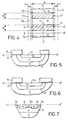
- Figure 4 shows a plan view of the surface of part of an example of a device according to the present invention before the gate dielectric and source metallisation layers have been applied;
- Figure 5 shows a section through A-A' of Figure 4;
- Figure 6 shows a corresponding section through B-B'; and
- Figure 7 a section through C-C' of Figure 4.
- Figures 8-10 show the directions of the majority current flow in the p-base regions 12 and 12a.
- Figure 8 shows the same basic section B-B' of Figure 6 but with the addition of the CVD oxide dielectric layer 16 and the source electrode layer 17.
- the arrows trace the path taken by the majority hole current arriving in a p-base strip 12 from the n-type substrate 11 in the vicinity where the section is cut. The flow of this current is only briefly through the thickness of the p-base strip 12 and then continues laterally in the reinforced p + segmented region 12a of relatively high conductivity where it runs parallel to the source-base junction and hence no significant bias is caused to occur across the source-base junction.
- Figure 9 is essentially as the section C-C' of Figure 4 shown in Figure 7 and the arrows trace the path taken by the majority hole current arriving in a p-base strip 12 from the n-type substrate 11 in the vicinity where this section is cut.
- the lateral path (i.e. horizontal displacement) taken by the majority current which is parallel to the axis of the p-base strip 12 is never more than half the width of one segment of the n + -source region, dimension W in Figure 9.
- Dimension W (the separation of the segmented p + - regions 12a along p-base strips 12) is preferably not more than 15 x 10 -6 m, such as not more than 10 x 10 -6 m or 5 x 10 -6 m. This is an easily controlled dimension, not dependent on mask registration accuracy.
- Figure 10 shows a combination in plan view of the majority carrier current flows shown in Figures 8 and 9.
- a strip 12 the segmented regions 12a and the n + -source regions 13 each have a margin of width on each side towards the boundaries of the strip (the margin of width of each n + -source region 13 on each side being L).
- the margins of width for regions 12a and 13 are substantially the same.
- the length of the edge of each of regions 12a parallel to the direction of its strip i.e. its width D
- each channel region 22 is L and the effective total useful width of each channel region 22 in the device will be greater than the sum of the widths W of the n + -source segmented regions 13 because of the divergence of the electron current from the sides of each n + -source segmented region 13 as it flows through the channel to the n-substrate 11.
- Figures 11 and 12 (a dimensioned version of Figure 9) give examples of typical (but not exclusive) dimensions for a structure according to the invention with reference numerals as used for Figure 3.
- the respective widths of the p-base strips 12, the p + reinforced segmented regions 12a of the p-base strips 12 and the n + -source segmented regions 13 are each defined by the same window 19 in the oxide/polysilicon layers.
- the only alignment required for the lines of n + -source segmented regions 13 running perpendicular to the p-base strips 12 is at their extreme ends which can be arranged to fall on a wider, inactive part of the p-base, thereby permitting a relaxed tolerance of registration.
- the extent of the p + reinforced segmented regions 12a of the p-base is fully defined by the combination of the first p-base strip window and the n-source mask.
- a further advantage is a good resistance to parasitic thyristor latching with less loss of effective active device area or other performance compromises than in the prior art designs discussed above.
- a yet further advantage is that since the p + contact region of the p-base does not run parallel to the edge of the gate, the window in the gate oxide does not have to accommodate the width of the p + region diffusion (including its lateral diffusion length around the edge of the window) thus permitting the gap between the two channel regions to be reduced compared to the prior art. This in turn enables the overall cell width to be less, thereby improving the proportion of active to inactive area of the device.
- This source side structure can be combined with any of the known anode structures currently used be they punch-through or non-punch-through, n- buffer, p- anode or shorted anode designs.
- the treatment of the p-base diffusion also influences the dimensions shown in Figure 11.
- the constraints on this p diffusion are that the total charge under the n + -source be sufficient to stop punch-through of the depletion region in the blocking state.
- the concentration at the p-base/n + -source intercept must be low enough to ensure an appropriate threshold voltage for channel formation.
- the worst case for dimensioning the device occurs when the peak dopant concentration in the p-base is located at the surface.
- any means of putting the peak dopant concentration subsurface for example a higher energy implant or an opposing threshold adjusting implant, allows for a greater n + -source width, since the sheet resistance under the source can be lowered to allow for a higher hole current before the onset of latching.
- n-source implant/p + implant can be commuted provided that the p + implant is masked and the implanted p + charge is greater than the implanted n + -source charge.
- the p + implant is then masked and the n + -source is self-aligned (i.e. determined by the combination of the first p-base strip mask and the p + implant mask) putting the p + reinforced region deeper rather than shallower (as shown in Figure 7) compared to the n + -source.
Landscapes
- Thyristors (AREA)
- Bipolar Transistors (AREA)
Applications Claiming Priority (2)
| Application Number | Priority Date | Filing Date | Title |
|---|---|---|---|
| GBGB9625839.7A GB9625839D0 (en) | 1996-12-12 | 1996-12-12 | Semiconductor switching devices |
| GB9625839 | 1996-12-12 |
Publications (2)
| Publication Number | Publication Date |
|---|---|
| EP0848430A2 true EP0848430A2 (de) | 1998-06-17 |
| EP0848430A3 EP0848430A3 (de) | 1999-01-13 |
Family
ID=10804342
Family Applications (1)
| Application Number | Title | Priority Date | Filing Date |
|---|---|---|---|
| EP97307163A Withdrawn EP0848430A3 (de) | 1996-12-12 | 1997-09-15 | Bipolartransistor mit isoliertem Gate |
Country Status (4)
| Country | Link |
|---|---|
| US (1) | US6147382A (de) |
| EP (1) | EP0848430A3 (de) |
| JP (1) | JPH10229192A (de) |
| GB (1) | GB9625839D0 (de) |
Cited By (2)
| Publication number | Priority date | Publication date | Assignee | Title |
|---|---|---|---|---|
| WO2001031709A1 (en) * | 1999-10-22 | 2001-05-03 | Semiconductor Components Industries, L.L.C. | Semiconductor device with a single base region and method therefor |
| WO2000044031A3 (de) * | 1999-01-25 | 2001-07-19 | Infineon Technologies Ag | Leistungstransistoranordnung mit hoher spannungsfestigkeit |
Families Citing this family (3)
| Publication number | Priority date | Publication date | Assignee | Title |
|---|---|---|---|---|
| US6351009B1 (en) * | 1999-03-01 | 2002-02-26 | Fairchild Semiconductor Corporation | MOS-gated device having a buried gate and process for forming same |
| JP5119589B2 (ja) * | 2005-11-04 | 2013-01-16 | 富士電機株式会社 | 半導体装置 |
| US8558275B2 (en) * | 2007-12-31 | 2013-10-15 | Alpha And Omega Semiconductor Ltd | Sawtooth electric field drift region structure for power semiconductor devices |
Family Cites Families (13)
| Publication number | Priority date | Publication date | Assignee | Title |
|---|---|---|---|---|
| EP0060912B1 (de) * | 1981-03-24 | 1986-10-22 | Siemens Aktiengesellschaft | Thyristor mit einem abschaltbaren Emitter-Kurzschluss |
| US5262336A (en) * | 1986-03-21 | 1993-11-16 | Advanced Power Technology, Inc. | IGBT process to produce platinum lifetime control |
| JPH07120794B2 (ja) * | 1986-07-09 | 1995-12-20 | 株式会社東芝 | Mos型半導体装置 |
| JPH01140773A (ja) * | 1987-11-27 | 1989-06-01 | Hitachi Ltd | 絶縁ゲート形トランジスタ |
| US4963950A (en) * | 1988-05-02 | 1990-10-16 | General Electric Company | Metal oxide semiconductor gated turn-off thyristor having an interleaved structure |
| US4994871A (en) * | 1988-12-02 | 1991-02-19 | General Electric Company | Insulated gate bipolar transistor with improved latch-up current level and safe operating area |
| JPH02312280A (ja) * | 1989-05-26 | 1990-12-27 | Mitsubishi Electric Corp | 絶縁ゲート型バイポーラトランジスタ |
| JP3321185B2 (ja) * | 1990-09-28 | 2002-09-03 | 株式会社東芝 | 高耐圧半導体装置 |
| JPH05206470A (ja) * | 1991-11-20 | 1993-08-13 | Nec Corp | 絶縁ゲート型電界効果トランジスタ |
| DE4315178A1 (de) * | 1993-05-07 | 1994-11-10 | Abb Management Ag | IGBT mit selbstjustierender Kathodenstruktur sowie Verfahren zu dessen Herstellung |
| US5581100A (en) * | 1994-08-30 | 1996-12-03 | International Rectifier Corporation | Trench depletion MOSFET |
| US5767555A (en) * | 1995-03-09 | 1998-06-16 | Hitachi, Ltd. | Compound semiconductor device controlled by MIS gate, driving method therefor and electric power conversion device using the compound semiconductor device and the driving method |
| US5703383A (en) * | 1995-04-11 | 1997-12-30 | Kabushiki Kaisha Toshiba | Power semiconductor device |
-
1996
- 1996-12-12 GB GBGB9625839.7A patent/GB9625839D0/en active Pending
-
1997
- 1997-09-15 EP EP97307163A patent/EP0848430A3/de not_active Withdrawn
- 1997-10-17 US US08/953,050 patent/US6147382A/en not_active Expired - Fee Related
- 1997-11-13 JP JP9312154A patent/JPH10229192A/ja active Pending
Cited By (2)
| Publication number | Priority date | Publication date | Assignee | Title |
|---|---|---|---|---|
| WO2000044031A3 (de) * | 1999-01-25 | 2001-07-19 | Infineon Technologies Ag | Leistungstransistoranordnung mit hoher spannungsfestigkeit |
| WO2001031709A1 (en) * | 1999-10-22 | 2001-05-03 | Semiconductor Components Industries, L.L.C. | Semiconductor device with a single base region and method therefor |
Also Published As
| Publication number | Publication date |
|---|---|
| US6147382A (en) | 2000-11-14 |
| JPH10229192A (ja) | 1998-08-25 |
| GB9625839D0 (en) | 1997-01-29 |
| EP0848430A3 (de) | 1999-01-13 |
Similar Documents
| Publication | Publication Date | Title |
|---|---|---|
| JP5357370B2 (ja) | 半導体デバイス | |
| US11923450B2 (en) | MOSFET in SiC with self-aligned lateral MOS channel | |
| EP0801425B1 (de) | Halbleiteranordnung mit isoliertem Gate und Verfahren zur Herstellung | |
| EP1895595B1 (de) | Halbleitervorrichtung und elektrische Stromwandlervorrichtung | |
| EP0633611B1 (de) | Halbleiteranordnung mit einer Bipolarfeldeffektanordnung mit isoliertem Gate | |
| US6091086A (en) | Reverse blocking IGBT | |
| CN115699328A (zh) | 具有分段沟槽和屏蔽件的沟槽功率器件 | |
| US5169793A (en) | Method of making an insulated gate bipolar transistor having gate shield region | |
| JP3417013B2 (ja) | 絶縁ゲート型バイポーラトランジスタ | |
| EP0224269A2 (de) | Lateraler Transistor mit isoliertem Gate mit Latch-up-Festigkeit | |
| US20030057478A1 (en) | Mos-gated power semiconductor device | |
| US4639762A (en) | MOSFET with reduced bipolar effects | |
| EP0159663A2 (de) | Thyristoren, Feldeffekttransistoren mit isoliertem Gate und MOSFETs hoher Dichte gesteuert durch eine in einer V-Nut angebrachte MOS-Struktur und Verfahren zur Herstellung | |
| JPH08264764A (ja) | 半導体装置 | |
| EP0810671A2 (de) | Halbleiterbauelement vom Isolationsgate-Bipolartransistortyp | |
| US20240234567A1 (en) | Buried shield structures for power semiconductor devices including segmented support shield structures for reduced on-resistance and related fabrication methods | |
| KR20000029577A (ko) | 선형전류-전압특성을가지는반도체부품 | |
| WO2012017227A1 (en) | Semiconductor device | |
| US5381025A (en) | Insulated gate thyristor with gate turn on and turn off | |
| US7332771B2 (en) | Trench-gate semiconductor devices | |
| US20240234507A1 (en) | Buried shield structures for power semiconductor devices and related fabrication methods | |
| EP0540017B1 (de) | MOS-Gate-kontrollierter Thyristor | |
| US6147382A (en) | Semiconductor switching device with segmented sources | |
| WO1991003078A1 (en) | Insulated gate thyristor with gate turn on and turn off | |
| US5223732A (en) | Insulated gate semiconductor device with reduced based-to-source electrode short |
Legal Events
| Date | Code | Title | Description |
|---|---|---|---|
| PUAI | Public reference made under article 153(3) epc to a published international application that has entered the european phase |
Free format text: ORIGINAL CODE: 0009012 |
|
| AK | Designated contracting states |
Kind code of ref document: A2 Designated state(s): CH DE FR LI |
|
| PUAL | Search report despatched |
Free format text: ORIGINAL CODE: 0009013 |
|
| AK | Designated contracting states |
Kind code of ref document: A3 Designated state(s): AT BE CH DE DK ES FI FR GB GR IE IT LI LU MC NL PT SE |
|
| RAP1 | Party data changed (applicant data changed or rights of an application transferred) |
Owner name: WESTCODE SEMICONDUCTORS LIMITED |
|
| 17P | Request for examination filed |
Effective date: 19990707 |
|
| AKX | Designation fees paid |
Free format text: CH DE FR LI |
|
| STAA | Information on the status of an ep patent application or granted ep patent |
Free format text: STATUS: THE APPLICATION IS DEEMED TO BE WITHDRAWN |
|
| 18D | Application deemed to be withdrawn |
Effective date: 20040401 |