EP0867944A2 - Dispositif semi-conducteur composé et méthode de contrÔle de ses caractéristiques - Google Patents
Dispositif semi-conducteur composé et méthode de contrÔle de ses caractéristiques Download PDFInfo
- Publication number
- EP0867944A2 EP0867944A2 EP98105342A EP98105342A EP0867944A2 EP 0867944 A2 EP0867944 A2 EP 0867944A2 EP 98105342 A EP98105342 A EP 98105342A EP 98105342 A EP98105342 A EP 98105342A EP 0867944 A2 EP0867944 A2 EP 0867944A2
- Authority
- EP
- European Patent Office
- Prior art keywords
- surface area
- electrodes
- semiconductor device
- compound semiconductor
- resistivity
- Prior art date
- Legal status (The legal status is an assumption and is not a legal conclusion. Google has not performed a legal analysis and makes no representation as to the accuracy of the status listed.)
- Ceased
Links
Images



Classifications
-
- H—ELECTRICITY
- H10—SEMICONDUCTOR DEVICES; ELECTRIC SOLID-STATE DEVICES NOT OTHERWISE PROVIDED FOR
- H10D—INORGANIC ELECTRIC SEMICONDUCTOR DEVICES
- H10D30/00—Field-effect transistors [FET]
- H10D30/60—Insulated-gate field-effect transistors [IGFET]
-
- H—ELECTRICITY
- H10—SEMICONDUCTOR DEVICES; ELECTRIC SOLID-STATE DEVICES NOT OTHERWISE PROVIDED FOR
- H10P—GENERIC PROCESSES OR APPARATUS FOR THE MANUFACTURE OR TREATMENT OF DEVICES COVERED BY CLASS H10
- H10P74/00—Testing or measuring during manufacture or treatment of wafers, substrates or devices
- H10P74/20—Testing or measuring during manufacture or treatment of wafers, substrates or devices characterised by the properties tested or measured, e.g. structural or electrical properties
- H10P74/207—Electrical properties, e.g. testing or measuring of resistance, deep levels or capacitance-voltage characteristics
-
- H—ELECTRICITY
- H10—SEMICONDUCTOR DEVICES; ELECTRIC SOLID-STATE DEVICES NOT OTHERWISE PROVIDED FOR
- H10D—INORGANIC ELECTRIC SEMICONDUCTOR DEVICES
- H10D84/00—Integrated devices formed in or on semiconductor substrates that comprise only semiconducting layers, e.g. on Si wafers or on GaAs-on-Si wafers
- H10D84/80—Integrated devices formed in or on semiconductor substrates that comprise only semiconducting layers, e.g. on Si wafers or on GaAs-on-Si wafers characterised by the integration of at least one component covered by groups H10D12/00 or H10D30/00, e.g. integration of IGFETs
- H10D84/82—Integrated devices formed in or on semiconductor substrates that comprise only semiconducting layers, e.g. on Si wafers or on GaAs-on-Si wafers characterised by the integration of at least one component covered by groups H10D12/00 or H10D30/00, e.g. integration of IGFETs of only field-effect components
- H10D84/83—Integrated devices formed in or on semiconductor substrates that comprise only semiconducting layers, e.g. on Si wafers or on GaAs-on-Si wafers characterised by the integration of at least one component covered by groups H10D12/00 or H10D30/00, e.g. integration of IGFETs of only field-effect components of only insulated-gate FETs [IGFET]
-
- H—ELECTRICITY
- H10—SEMICONDUCTOR DEVICES; ELECTRIC SOLID-STATE DEVICES NOT OTHERWISE PROVIDED FOR
- H10D—INORGANIC ELECTRIC SEMICONDUCTOR DEVICES
- H10D84/00—Integrated devices formed in or on semiconductor substrates that comprise only semiconducting layers, e.g. on Si wafers or on GaAs-on-Si wafers
- H10D84/80—Integrated devices formed in or on semiconductor substrates that comprise only semiconducting layers, e.g. on Si wafers or on GaAs-on-Si wafers characterised by the integration of at least one component covered by groups H10D12/00 or H10D30/00, e.g. integration of IGFETs
- H10D84/82—Integrated devices formed in or on semiconductor substrates that comprise only semiconducting layers, e.g. on Si wafers or on GaAs-on-Si wafers characterised by the integration of at least one component covered by groups H10D12/00 or H10D30/00, e.g. integration of IGFETs of only field-effect components
- H10D84/83—Integrated devices formed in or on semiconductor substrates that comprise only semiconducting layers, e.g. on Si wafers or on GaAs-on-Si wafers characterised by the integration of at least one component covered by groups H10D12/00 or H10D30/00, e.g. integration of IGFETs of only field-effect components of only insulated-gate FETs [IGFET]
- H10D84/83138—Integrated devices formed in or on semiconductor substrates that comprise only semiconducting layers, e.g. on Si wafers or on GaAs-on-Si wafers characterised by the integration of at least one component covered by groups H10D12/00 or H10D30/00, e.g. integration of IGFETs of only field-effect components of only insulated-gate FETs [IGFET] the IGFETs characterised by having different shapes or dimensions of their gate conductors
-
- H—ELECTRICITY
- H10—SEMICONDUCTOR DEVICES; ELECTRIC SOLID-STATE DEVICES NOT OTHERWISE PROVIDED FOR
- H10P—GENERIC PROCESSES OR APPARATUS FOR THE MANUFACTURE OR TREATMENT OF DEVICES COVERED BY CLASS H10
- H10P74/00—Testing or measuring during manufacture or treatment of wafers, substrates or devices
- H10P74/27—Structural arrangements therefor
- H10P74/277—Circuits for electrically characterising or monitoring manufacturing processes, e.g. circuits in tested chips or circuits in testing wafers
Definitions
- the present invention generally relates to a compound semiconductor device and a method for controlling characteristics of the same, and more particularly, the present invention relates to a compound semiconductor device and a method for controlling characteristics of the same to obtain a homogeneous threshold voltage among plural transistors or a homogeneous resistivity among plural resistors.
- a conventional electronic component includes a plurality of field effect transistors and a plurality of resistors.
- the plurality of field effect transistors respectively have gates of different widths. Improved controllability of threshold voltages of the field effect transistors is important in stabilizing the performance of the electronic component.
- the conventional method for controlling a threshold voltage of the field effect transistor is as follows:
- First and second field effect transistors are simultaneously formed on the semiconductor chip.
- the second field effect transistor serves as a monitor for observing the process steps. That is, the threshold voltage of the second field effect transistor is measured after the ion-implantation for establishing a desired threshold voltage is completed. When the measured threshold voltage is lower than the desired value, the ion-implantation for establishing the desired threshold voltage is carried out for the second time.
- An object of the present invention is to provide a compound semiconductor device that can precisely control a threshold voltage of a field effect transistor.
- a compound semiconductor device comprising a first field effect transistor defining a first active region in a semi-insulating substrate, the first field effect transistor having a first ohmic source electrode and a first ohmic drain electrode extending over the first active region, a second field effect transistor defining a second active region in the semi-insulating substrate, the second field effect transistor having a second ohmic source electrode and a second ohmic drain electrode extending over the second active region, and wherein, a ratio of a difference between a surface area of the first active region and a combined surface area of the first source and drain ohmic electrodes to the combined surface area of the first source and drain ohmic electrodes is the same as a ratio of a difference between a surface area of the second active region and a combined surface area of the second source and drain ohmic electrodes to the combined surface area of the second source and drain ohmic electrodes.
- An object of the present invention is to provide a compound semiconductor device that can precisely control a resistivity of the resistor.
- a compound semiconductor device comprising a first resistor defining a first resistivity region in a semi-insulating substrate, the first resistor having a first pair electrodes extending over the first resistivity region, a second resistor defining a second resistivity region in the semi-insulating substrate, the second resistor having a second pair electrodes extending over the second resistivity region, and wherein, a ratio of a difference between a surface area of the first resistivity region and a combined surface area of the first electrodes to the combined surface area of the first electrodes is the same as a ratio of a difference between a surface area of the second resistivity region and a combined surface area of the second pair electrodes to the combined surface area of the second pair electrodes.
- An object of the present invention is to provide a method for controlling a a characteristics of a compound semiconductor device that can satisfy homogeneity of the threshold voltages of the plurality of the field effect transistors at every substrate if a plurality, of wafers treat using a single wafer processing.
- a method for controlling a a characteristics of a compound semiconductor device comprising the steps of providing a first field effect transistor defining a first active region in a semi-insulating substrate, the first field effect transistor having a first ohmic source electrode and a first ohmic drain electrode extending over the first active region, a second field effect transistor defining a second active region in the semi-insulating substrate, the second field effect transistor having a second ohmic source electrode and a second ohmic drain electrode extending over the second active region, wherein, a ratio of a difference between a surface area of the first active region and a combined surface area of the first source and drain ohmic electrodes to the combined surface area of the first source and drain ohmic electrodes is the same as a ratio of a difference between a surface area of the second active region and a combined surface area of the second source and drain ohmic electrodes to the combined surface area of the second source and drain
- a method for controlling a a characteristics of a compound semiconductor device comprising the steps of providing a first field effect transistor defining a first active region in a first semi-insulating substrate, the first field effect transistor having a first ohmic source electrode and a first ohmic drain electrode extending over the first active region, a second field effect transistor defining a second active region in a second semi-insulating substrate, the second field effect transistor having a second ohmic source electrode and a second ohmic drain electrode extending over the second active region, wherein, a ratio of a difference between a surface area of the first active region and a combined surface area of the first source and drain ohmic electrodes to the combined surface area of the first source and drain ohmic electrodes is the same as a ratio of a difference between a surface area of the second active region and a combined surface area of the second source and drain ohmic electrodes to the combined surface area of the second
- An object of the present invention is to provide a method for controlling a a characteristics of a compound semiconductor device that can satisfy homogeneity of the resistivity of the plurality of the resistors at every substrate if a plurality of wafers treat using a single wafer processing.
- a method for controlling a a characteristics of a compound semiconductor device comprising the steps of providing a first resistor defining a first resistivity region in a semi-insulating substrate, the first resistor having a first pair electrodes extending over the first resistivity region, a second resistor defining a second resistivity region in the semi-insulating substrate, the second resistor having a second pair electrodes extending over the second resistivity region, wherein, a ratio of a difference between a surface area of the first resistivity region and a combined surface area of the first electrodes to the combined surface area of the first electrodes is the same as a ratio of a difference between a surface area of the second resistivity region and a combined surface area of the second pair electrodes to the combined surface area of the second pair electrodes, measuring a resistivity of the second resistor, and controlling the resistivity of the first resistor based on the measured result.
- a method for controlling a a characteristics of a compound semiconductor device comprising the steps of providing a first resistor defining a first resistivity region in a first semi-insulating substrate, the first resistor having a first pair electrodes extending over the first resistivity region, a second resistor defining a second resistivity region in a second semi-insulating substrate, the second resistor having a second pair electrodes extending over the second resistivity region, and wherein, a ratio of a difference between a surface area of the first resistivity region and a combined surface area of the first electrodes to the combined surface area of the first electrodes is the same as a ratio of a difference between a surface area of the second resistivity region and a combined surface area of the second pair electrodes to the combined surface area of the second pair electrodes, measuring a resistivity of the second resistor, and controlling the resistivity of the first resistor based on the measured result.
- Fig. 1 is a plane view showing the compound semiconductor device according to the first preferred embodiment of the present invention.
- the compound semiconductor device includes a first field effect transistor (FET) 100 and a second field effect transistor (FET) 101 formed on a GaAs substrate 11.
- the first FET 100 serves as a monitor for observing the process steps.
- the first FET 100 includes a first active region 13a, first source and drain ohmic electrodes 17a and 18a formed on source and drain regions (not shown) in the first active region 13a, and a first gate electrode 19a formed on the first active region 13a.
- the second FET 101 includes a second active region 13b, second source and drain ohmic electrodes 17b and 18b formed on source and drain regions (not shown) in the second active region 13b, and a second gate electrode 19b formed on the second active region 13b.
- Each devices is characterized by an " electrode ratio" which is defined herein as the ratio of a difference between a surface area of the active region and a combined overlapping surface area of the source and drain regions (i.e, a surface portion of each of the source and drain electrodes which overlaps the active region) to the combined overlapping surface area of the source and drain regions.
- the first FET 100 is characterized by a first electrode ratio a : b of (a) a difference between a surface area of the first active region 13a and a combined overlapping surface area of the first source and drain ohmic electrodes 17a and 18a to (b) the combined overlapping surface area of the first source and drain ohmic electrodes 17a and 18a.
- the second FET 101 is characterized by a second electrode ratio c : d of (c) a difference between a surface area of the second active region 13b and a combined overlapping surface area of the second source and drain ohmic electrodes 17b and 18b to (d) the combined overlapping surface area of the second source and drain ohmic electrodes 17b and 18b.
- the first electrode ratio a/b is substantially the same as the second electrode ratio c/d.
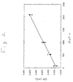
- Fig. 2 is a diagram showing measured relations between the threshold voltage and the electrode ratio of the devices.
- the plurality of FETs used for the measurements had respectively different gate widths (50 ⁇ m, 100 ⁇ m, 150 ⁇ m and 200 ⁇ m ).
- the plurality of FETs were also formed so as to have the same electrode ratios.
- all of the plurality of FETs have substantially the same threshold voltage as a result of forming the plurality of FETs with the same electrode ratio, even though the plurality of FETs have respectively different gate widths.
- the electrode ratio is in proportion to the threshold voltage of the FETs.
- the plurality of FETs are respectively formed so as to have the same electrode ratio. As a result, all of the plurality of FETs have substantially the same threshold voltage. Further, by confirming the respective electrode ratios of the plurality of FETs in advance, the first preferred embodiment can precisely acheive the desired threshold voltages based on a diagram showing the relation between the threshold voltage and the electrode ratios.
- Fig. 3A and B are cross-sectional views showing the steps of the method for controlling characteristics of the compound semiconductor device according to the first preferred embodiment of the present invention.
- the compound semiconductor device includes the formation region of a first field effect transistor (FET) 100 and the formation region of a second field effect transistor (FET) 101 provided on a GaAs substrate 11.
- a first active region 13a, source and drain regions 21a and 23a in the first active region 13a for the first FET 100 and a second active region 13b, source and drain regions 21b and 23b in the second active region 13b for the second FET 101 respectively are formed by implanting Si as an n-type dopant and then annealing for an activation.
- First source and drain ohmic electrodes 17a and 18a are then respectively formed on the source and drain regions 21a and 23a, and second source and drain ohmic electrodes 17b and 18b are then respectively formed on the source and drain regions 21b and 23b.
- the electrodes are preferably a layer comprising an Au-Ge alloy layer and an Au-Ni alloy layer.
- a photo-resist pattern 25 is formed on the entire substrate so as to expose upper surfaces of the electrodes 17a, 17b, 18a and so as to expose the predetermined portion of the first and second active regions 13a and 13b.
- the predetermined portion corresponds with formations regions of gate electrodes for the first and second FET 100 and 101.
- the first FET 100 has a first electrode a : b ratio of (a) a difference between a surface area of the first active region 13a and a combined overlapping surface area of the first source and drain ohmic electrodes 17a and 18a to (b) the combined overlapping surface area of the first source and drain ohmic electrodes 17a and 18a.
- the second FET 101 has a second electrode ratio c : d of (c) a difference between a surface area of the second active region 13b and a combined overlapping surface area of the second source and drain ohmic electrodes 17b and 18b to (d) the combined overlapping surface area of the second source and drain ohmic electrodes 17b and 18b.
- the first electrode ratio a/b is same as the second electrode ratio c/d.
- the first and second active regions 13a and 13b are etched to control a threshold voltage using the photo-resist pattern 25. Then, the threshold voltage of the first FET 100 is measured using probe needles. When the measured threshold voltage is lower than a predetermined value, the etching process is carried out again.
- the threshold of second FET 101 is indirectly controlled using the first FET 100 as a monitor.
- the plurality of FETs respectively are formed so as to have a same electrode ratio of a difference between a surface area of the active region and a combined overlapping surface area of the source and drain ohmic electrodes to the combined surface area of the source and drain ohmic electrodes.
- all of the plurality of FETs have substantially the same threshold voltage.
- the first preferred method for controlling desired characteristics of a compound semiconductor device can precisely achieve the respective desired voltages based on a diagram showing a relation between threshold voltages and electrode ratios.
- the first preferred method for controlling characteristics of a compound semiconductor device can achieve homogeneity of the threshold voltages of the plurality of the field effect transistors at every substrate in the case where a plurality of wafers are treated using a single wafer processing.
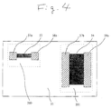
- Fig. 4 is a plane view showing the compound semiconductor device according to a second preferred embodiment of the present invention.
- the compound semiconductor device include a first resistor 200 which is used as a monitor and a second resistor 201 formed on a GaAs substrate 11.
- the first resistor 200 includes a first resistivity region 53 and a first pair of electrodes 57a and 58a formed on the first resistivity region 53.
- the second resistor 201 includes a second resistivity region 54, a second pair of electrodes 57b and 58b formed on the second resistivity region 54.
- the first resistor 200 has a first electrode ratio which is defined as a ratio of a difference between a surface area of the first resistivity region 53 and a combined overlapping surface area of the first pair electrodes 57a and 58a to the combined overlapping surface area of the first pair of electrodes 57a and 58a.
- the second resistor 201 has a second electrode ratio of a difference between a surface area of the second resistivity region 54 and a combined overlapping surface area of the second pair of electrodes 57b and 58b to the combined overlapping surface area of the second pair of electrodes 57b and 58b.
- the first ratio is the same as the second ratio.
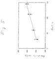
- Fig. 5 is a diagram showing relations between the resistivity of the electrode and electrode ratio of plural resistors.
- the plurality of resistors used for the measurement had respectively different resistivity region sizes.
- the size of the resistivity region corresponds with the extending direction between the pair electrodes (50 ⁇ m, 100 ⁇ m, 150 ⁇ m and 200 ⁇ m ).
- the plurality of resistors were also formed to as to have the same electrode ratios.
- all of the plurality of resistors have substantially the same resistivity as a result of forming the plurality of resistors with the same electrode ratio, even though the plurality of resistors have respectively different resistivity region sizes.
- the electrode ratio is in proportion to the resistivity of the resistors.
- the plurality of resistors are respectively formed so as to have a same electrode ratio. As a result, all of the plurality of resistors have substantially the same resistivity. Further, by confirming the respective electrode ratios of the plurality of resistors in advance, the second preferred embodiment precisely can achieve the desired resistivity based on a diagram showing a relation between resistivity and electrode ratio.
- Fig. 6A and B are cross-sectional views showing the steps of a method for controlling characteristics of a compound semiconductor device according to a second preferred embodiment of the present invention.
- the compound semiconductor device includes a formation region of a first resistor 110 used as a monitor and a formation region of a second resistor 111 provided on a GaAs substrate 11.
- First and second resistivity regions 23a and 23b are formed by implanting Si as an n-type dopant and then annealing for activation.
- First pair electrodes 27a and 28a are then formed on the resistivity region 23a, and second pair electrodes 27b and 28b are then formed on the resistivity regions 23b.
- Materials of the electrodes are preferably Au-Ge alloy/Ni/Au.
- a photo-resist pattern 35 is formed on the entire substrate so as to expose upper surfaces of the electrodes 27a, 28a, 27b and 28b and the first and second resistivity regions 23a and 23b.
- the first resistor 110 has a first electrode ratio of a difference between a surface area of the first resistivity region 23a and a combined overlapping surface area of the first pair of electrodes 27a and 28a to the combined overlapping surface area of the first pair of electrodes 27a and 28a.
- the second resistor 111 has a second electrode ratio of a difference between a surface area of the second resistivity region 23b and a combined overlapping surface area of the second par of electrodes 27b and 28b to the combined overlapping surface area of the second pair of electrodes 27b and 28b.
- the first electrode ratio is same as the second electrode ratio.
- the first and second resistivity regions 23a and 23b are etched to control a resistivity using the photo-resist pattern 25. Then, the resistivity of the first resistor 110 used as a monitor is measured using probe needles. When the measured resistivity is lower than a predetermined value, the etching process is carried out again.
- the second resistor 111 indirectly controls the resistivity using the first resistor 110 for a monitor.
- the plurality of resistors respectively are formed so as to have the same electrode ratio. As a result, all of the plurality of resistors have substantially the same resistivity. Further, by confirming the respective ratio of a plurality of resistors in advance, the second preferred method for controlling characteristics of a compound semiconductor device can precisely achieve the desired resistivity based on a diagram showing a relation between resistivity and electrode ratio.
- the second preferred method for controlling characteristics of a compound semiconductor device can achieve homogeneity of the resistivity of the plurality of the resistors at every substrate in the case where a plurality of wafers are treated using a single wafer processing.
Landscapes
- Junction Field-Effect Transistors (AREA)
Applications Claiming Priority (3)
| Application Number | Priority Date | Filing Date | Title |
|---|---|---|---|
| JP07339697A JP4084436B2 (ja) | 1997-03-26 | 1997-03-26 | 化合物半導体装置の特性の制御方法 |
| JP7339697 | 1997-03-26 | ||
| JP73396/97 | 1997-03-26 |
Publications (2)
| Publication Number | Publication Date |
|---|---|
| EP0867944A2 true EP0867944A2 (fr) | 1998-09-30 |
| EP0867944A3 EP0867944A3 (fr) | 1999-08-04 |
Family
ID=13517008
Family Applications (1)
| Application Number | Title | Priority Date | Filing Date |
|---|---|---|---|
| EP98105342A Ceased EP0867944A3 (fr) | 1997-03-26 | 1998-03-24 | Dispositif semi-conducteur composé et méthode de contrÔle de ses caractéristiques |
Country Status (4)
| Country | Link |
|---|---|
| US (3) | US6265728B1 (fr) |
| EP (1) | EP0867944A3 (fr) |
| JP (1) | JP4084436B2 (fr) |
| KR (1) | KR100370987B1 (fr) |
Families Citing this family (5)
| Publication number | Priority date | Publication date | Assignee | Title |
|---|---|---|---|---|
| JP2000277724A (ja) * | 1999-03-26 | 2000-10-06 | Nagoya Kogyo Univ | 電界効果トランジスタとそれを備えた半導体装置及びその製造方法 |
| TW577124B (en) * | 2002-12-03 | 2004-02-21 | Mosel Vitelic Inc | Method for estimating the forming thickness of the oxide layer and determining whether the pipes occur leakages |
| JP3931153B2 (ja) * | 2003-04-24 | 2007-06-13 | 松下電器産業株式会社 | 半導体装置 |
| US20070282318A1 (en) * | 2006-05-16 | 2007-12-06 | Spooner Gregory J | Subcutaneous thermolipolysis using radiofrequency energy |
| US7785979B2 (en) * | 2008-07-15 | 2010-08-31 | International Business Machines Corporation | Integrated circuits comprising resistors having different sheet resistances and methods of fabricating the same |
Family Cites Families (16)
| Publication number | Priority date | Publication date | Assignee | Title |
|---|---|---|---|---|
| FR2280203A1 (fr) * | 1974-07-26 | 1976-02-20 | Thomson Csf | Procede d'ajustement de tension de seuil de transistors a effet de champ |
| US4215333A (en) * | 1978-10-02 | 1980-07-29 | National Semiconductor Corporation | Resistor termination |
| US4560583A (en) * | 1984-06-29 | 1985-12-24 | International Business Machines Corporation | Resistor design system |
| JPS6148768A (ja) * | 1984-08-17 | 1986-03-10 | Matsushita Electronics Corp | コンタクト抵抗の測定方法 |
| JPS63164260A (ja) | 1986-12-25 | 1988-07-07 | Mitsubishi Electric Corp | 半導体装置 |
| JPS63278361A (ja) | 1987-05-11 | 1988-11-16 | Sumitomo Electric Ind Ltd | 半導体装置と半導体装置の抵抗トリミング法 |
| JPH03229426A (ja) * | 1989-11-29 | 1991-10-11 | Texas Instr Inc <Ti> | 集積回路及びその製造方法 |
| JPH0482248A (ja) * | 1990-07-25 | 1992-03-16 | Sumitomo Electric Ind Ltd | 半導体装置の評価方法 |
| JPH0547798A (ja) * | 1991-01-31 | 1993-02-26 | Texas Instr Inc <Ti> | 抵抗性AlGaAsを有するGaAs FET |
| JPH04263466A (ja) | 1991-02-19 | 1992-09-18 | Fujitsu Ltd | 半導体装置の製造方法 |
| JP2734839B2 (ja) * | 1991-10-09 | 1998-04-02 | シャープ株式会社 | アルミニウム用エッチング液およびエッチング方法並びにアルミニウムエッチング製品 |
| JPH05218309A (ja) | 1992-02-04 | 1993-08-27 | Fujitsu Ltd | 半導体装置及びその製造方法 |
| JP2750992B2 (ja) * | 1992-08-12 | 1998-05-18 | 三菱電機株式会社 | 半導体装置およびその製造方法 |
| JPH06132319A (ja) | 1992-10-20 | 1994-05-13 | Japan Energy Corp | 半導体装置の製造方法 |
| JP3107681B2 (ja) * | 1993-06-29 | 2000-11-13 | 沖電気工業株式会社 | リセス構造fetのエッチング制御方法 |
| JPH0878439A (ja) * | 1994-09-05 | 1996-03-22 | Mitsubishi Electric Corp | 半導体装置の製造方法 |
-
1997
- 1997-03-26 JP JP07339697A patent/JP4084436B2/ja not_active Expired - Lifetime
-
1998
- 1998-03-19 US US09/044,009 patent/US6265728B1/en not_active Expired - Lifetime
- 1998-03-24 EP EP98105342A patent/EP0867944A3/fr not_active Ceased
- 1998-03-25 KR KR10-1998-0010332A patent/KR100370987B1/ko not_active Expired - Fee Related
-
2001
- 2001-06-05 US US09/873,208 patent/US6504185B2/en not_active Expired - Lifetime
-
2002
- 2002-11-21 US US10/300,848 patent/US6908777B2/en not_active Expired - Lifetime
Also Published As
| Publication number | Publication date |
|---|---|
| US6265728B1 (en) | 2001-07-24 |
| US20010028070A1 (en) | 2001-10-11 |
| US20030075727A1 (en) | 2003-04-24 |
| KR19980080662A (ko) | 1998-11-25 |
| JPH10270461A (ja) | 1998-10-09 |
| JP4084436B2 (ja) | 2008-04-30 |
| US6908777B2 (en) | 2005-06-21 |
| EP0867944A3 (fr) | 1999-08-04 |
| KR100370987B1 (ko) | 2003-07-16 |
| US6504185B2 (en) | 2003-01-07 |
Similar Documents
| Publication | Publication Date | Title |
|---|---|---|
| EP0225821B1 (fr) | Dispositif semi-conducteur à structure silicium sur isolant | |
| US8247286B2 (en) | Semiconductor device having transistor and method of manufacturing the same | |
| EP1103074A2 (fr) | Transistor a effet de champ a mos, a auto-alignement de grille et blindage enterre, et procede de fabrication correspondant | |
| DE102014112823B4 (de) | Halbleiterschalter mit integriertem Temperatursensor | |
| EP0359528A2 (fr) | Transistors à haute tension en couche mince | |
| US6091113A (en) | Semiconductor device with evaluation MISFET | |
| GB2230898A (en) | Field effect transistors | |
| EP0867944A2 (fr) | Dispositif semi-conducteur composé et méthode de contrÔle de ses caractéristiques | |
| US5360755A (en) | Method of manufacturing a dual field effect transistor | |
| US6136616A (en) | Method of forming semiconductor devices using gate electrode dimensions and dopant concentration for controlling drive current strength | |
| US4178603A (en) | Schottky transistor with low residual voltage | |
| US6472712B1 (en) | Semiconductor device with reduced transistor leakage current | |
| US5652451A (en) | Recessed gate field effect transistor | |
| KR101113358B1 (ko) | 에칭 방법 및 반도체 장치의 제조 방법 | |
| JP3107681B2 (ja) | リセス構造fetのエッチング制御方法 | |
| KR101053639B1 (ko) | 접합형 전계 효과 트랜지스터 소자 및 그 제조 방법 | |
| JPH11220124A (ja) | 半導体装置 | |
| US6362067B1 (en) | Accurate self-aligned resistor structure and method of making the same | |
| CA1133149A (fr) | Transistors a effet de champ | |
| KR100352419B1 (ko) | 트랜지스터를 구비한 반도체 장치 | |
| JPS6338264A (ja) | 電界効果トランジスタおよびその製造方法 | |
| JPH0620130B2 (ja) | Misトランジスタ及びその製造方法 | |
| JPH0612822B2 (ja) | 半導体装置 | |
| JP3017838B2 (ja) | 半導体装置およびその製造方法 | |
| GB1586423A (en) | Field-effect transistors |
Legal Events
| Date | Code | Title | Description |
|---|---|---|---|
| PUAI | Public reference made under article 153(3) epc to a published international application that has entered the european phase |
Free format text: ORIGINAL CODE: 0009012 |
|
| AK | Designated contracting states |
Kind code of ref document: A2 Designated state(s): DE FR GB |
|
| AX | Request for extension of the european patent |
Free format text: AL;LT;LV;MK;RO;SI |
|
| PUAL | Search report despatched |
Free format text: ORIGINAL CODE: 0009013 |
|
| RIC1 | Information provided on ipc code assigned before grant |
Free format text: 6H 01L 27/085 A, 6H 01L 27/095 B, 6H 01L 27/08 B, 6H 01L 25/03 B, 6H 01L 21/66 B, 6H 01L 101:00 Z |
|
| AK | Designated contracting states |
Kind code of ref document: A3 Designated state(s): AT BE CH DE DK ES FI FR GB GR IE IT LI LU MC NL PT SE |
|
| AX | Request for extension of the european patent |
Free format text: AL;LT;LV;MK;RO;SI |
|
| 17P | Request for examination filed |
Effective date: 19991004 |
|
| AKX | Designation fees paid |
Free format text: DE FR GB |
|
| 17Q | First examination report despatched |
Effective date: 20000619 |
|
| STAA | Information on the status of an ep patent application or granted ep patent |
Free format text: STATUS: THE APPLICATION HAS BEEN REFUSED |
|
| 18R | Application refused |
Effective date: 20071010 |