EP0881680A2 - Dispositif a semi-conducteur - Google Patents
Dispositif a semi-conducteur Download PDFInfo
- Publication number
- EP0881680A2 EP0881680A2 EP96940146A EP96940146A EP0881680A2 EP 0881680 A2 EP0881680 A2 EP 0881680A2 EP 96940146 A EP96940146 A EP 96940146A EP 96940146 A EP96940146 A EP 96940146A EP 0881680 A2 EP0881680 A2 EP 0881680A2
- Authority
- EP
- European Patent Office
- Prior art keywords
- lead frame
- power device
- region
- lead
- control device
- Prior art date
- Legal status (The legal status is an assumption and is not a legal conclusion. Google has not performed a legal analysis and makes no representation as to the accuracy of the status listed.)
- Granted
Links
Images


Classifications
-
- H—ELECTRICITY
- H10—SEMICONDUCTOR DEVICES; ELECTRIC SOLID-STATE DEVICES NOT OTHERWISE PROVIDED FOR
- H10W—GENERIC PACKAGES, INTERCONNECTIONS, CONNECTORS OR OTHER CONSTRUCTIONAL DETAILS OF DEVICES COVERED BY CLASS H10
- H10W72/00—Interconnections or connectors in packages
- H10W72/90—Bond pads, in general
-
- H—ELECTRICITY
- H10—SEMICONDUCTOR DEVICES; ELECTRIC SOLID-STATE DEVICES NOT OTHERWISE PROVIDED FOR
- H10W—GENERIC PACKAGES, INTERCONNECTIONS, CONNECTORS OR OTHER CONSTRUCTIONAL DETAILS OF DEVICES COVERED BY CLASS H10
- H10W72/00—Interconnections or connectors in packages
- H10W72/50—Bond wires
-
- H—ELECTRICITY
- H10—SEMICONDUCTOR DEVICES; ELECTRIC SOLID-STATE DEVICES NOT OTHERWISE PROVIDED FOR
- H10W—GENERIC PACKAGES, INTERCONNECTIONS, CONNECTORS OR OTHER CONSTRUCTIONAL DETAILS OF DEVICES COVERED BY CLASS H10
- H10W72/00—Interconnections or connectors in packages
- H10W72/071—Connecting or disconnecting
- H10W72/075—Connecting or disconnecting of bond wires
- H10W72/07541—Controlling the environment, e.g. atmosphere composition or temperature
- H10W72/07552—Controlling the environment, e.g. atmosphere composition or temperature changes in structures or sizes
-
- H—ELECTRICITY
- H10—SEMICONDUCTOR DEVICES; ELECTRIC SOLID-STATE DEVICES NOT OTHERWISE PROVIDED FOR
- H10W—GENERIC PACKAGES, INTERCONNECTIONS, CONNECTORS OR OTHER CONSTRUCTIONAL DETAILS OF DEVICES COVERED BY CLASS H10
- H10W72/00—Interconnections or connectors in packages
- H10W72/071—Connecting or disconnecting
- H10W72/075—Connecting or disconnecting of bond wires
- H10W72/07541—Controlling the environment, e.g. atmosphere composition or temperature
- H10W72/07553—Controlling the environment, e.g. atmosphere composition or temperature changes in shapes
-
- H—ELECTRICITY
- H10—SEMICONDUCTOR DEVICES; ELECTRIC SOLID-STATE DEVICES NOT OTHERWISE PROVIDED FOR
- H10W—GENERIC PACKAGES, INTERCONNECTIONS, CONNECTORS OR OTHER CONSTRUCTIONAL DETAILS OF DEVICES COVERED BY CLASS H10
- H10W72/00—Interconnections or connectors in packages
- H10W72/50—Bond wires
- H10W72/521—Structures or relative sizes of bond wires
- H10W72/527—Multiple bond wires having different sizes
-
- H—ELECTRICITY
- H10—SEMICONDUCTOR DEVICES; ELECTRIC SOLID-STATE DEVICES NOT OTHERWISE PROVIDED FOR
- H10W—GENERIC PACKAGES, INTERCONNECTIONS, CONNECTORS OR OTHER CONSTRUCTIONAL DETAILS OF DEVICES COVERED BY CLASS H10
- H10W72/00—Interconnections or connectors in packages
- H10W72/50—Bond wires
- H10W72/531—Shapes of wire connectors
- H10W72/537—Multiple bond wires having different shapes
-
- H—ELECTRICITY
- H10—SEMICONDUCTOR DEVICES; ELECTRIC SOLID-STATE DEVICES NOT OTHERWISE PROVIDED FOR
- H10W—GENERIC PACKAGES, INTERCONNECTIONS, CONNECTORS OR OTHER CONSTRUCTIONAL DETAILS OF DEVICES COVERED BY CLASS H10
- H10W72/00—Interconnections or connectors in packages
- H10W72/50—Bond wires
- H10W72/541—Dispositions of bond wires
- H10W72/5449—Dispositions of bond wires not being orthogonal to a side surface of the chip, e.g. fan-out arrangements
-
- H—ELECTRICITY
- H10—SEMICONDUCTOR DEVICES; ELECTRIC SOLID-STATE DEVICES NOT OTHERWISE PROVIDED FOR
- H10W—GENERIC PACKAGES, INTERCONNECTIONS, CONNECTORS OR OTHER CONSTRUCTIONAL DETAILS OF DEVICES COVERED BY CLASS H10
- H10W72/00—Interconnections or connectors in packages
- H10W72/50—Bond wires
- H10W72/541—Dispositions of bond wires
- H10W72/547—Dispositions of multiple bond wires
- H10W72/5475—Dispositions of multiple bond wires multiple bond wires connected to common bond pads at both ends of the wires
-
- H—ELECTRICITY
- H10—SEMICONDUCTOR DEVICES; ELECTRIC SOLID-STATE DEVICES NOT OTHERWISE PROVIDED FOR
- H10W—GENERIC PACKAGES, INTERCONNECTIONS, CONNECTORS OR OTHER CONSTRUCTIONAL DETAILS OF DEVICES COVERED BY CLASS H10
- H10W72/00—Interconnections or connectors in packages
- H10W72/50—Bond wires
- H10W72/551—Materials of bond wires
- H10W72/552—Materials of bond wires comprising metals or metalloids, e.g. silver
- H10W72/5522—Materials of bond wires comprising metals or metalloids, e.g. silver comprising gold [Au]
-
- H—ELECTRICITY
- H10—SEMICONDUCTOR DEVICES; ELECTRIC SOLID-STATE DEVICES NOT OTHERWISE PROVIDED FOR
- H10W—GENERIC PACKAGES, INTERCONNECTIONS, CONNECTORS OR OTHER CONSTRUCTIONAL DETAILS OF DEVICES COVERED BY CLASS H10
- H10W72/00—Interconnections or connectors in packages
- H10W72/50—Bond wires
- H10W72/551—Materials of bond wires
- H10W72/552—Materials of bond wires comprising metals or metalloids, e.g. silver
- H10W72/5524—Materials of bond wires comprising metals or metalloids, e.g. silver comprising aluminium [Al]
-
- H—ELECTRICITY
- H10—SEMICONDUCTOR DEVICES; ELECTRIC SOLID-STATE DEVICES NOT OTHERWISE PROVIDED FOR
- H10W—GENERIC PACKAGES, INTERCONNECTIONS, CONNECTORS OR OTHER CONSTRUCTIONAL DETAILS OF DEVICES COVERED BY CLASS H10
- H10W72/00—Interconnections or connectors in packages
- H10W72/50—Bond wires
- H10W72/59—Bond pads specially adapted therefor
-
- H—ELECTRICITY
- H10—SEMICONDUCTOR DEVICES; ELECTRIC SOLID-STATE DEVICES NOT OTHERWISE PROVIDED FOR
- H10W—GENERIC PACKAGES, INTERCONNECTIONS, CONNECTORS OR OTHER CONSTRUCTIONAL DETAILS OF DEVICES COVERED BY CLASS H10
- H10W72/00—Interconnections or connectors in packages
- H10W72/90—Bond pads, in general
- H10W72/921—Structures or relative sizes of bond pads
- H10W72/926—Multiple bond pads having different sizes
-
- H—ELECTRICITY
- H10—SEMICONDUCTOR DEVICES; ELECTRIC SOLID-STATE DEVICES NOT OTHERWISE PROVIDED FOR
- H10W—GENERIC PACKAGES, INTERCONNECTIONS, CONNECTORS OR OTHER CONSTRUCTIONAL DETAILS OF DEVICES COVERED BY CLASS H10
- H10W74/00—Encapsulations, e.g. protective coatings
-
- H—ELECTRICITY
- H10—SEMICONDUCTOR DEVICES; ELECTRIC SOLID-STATE DEVICES NOT OTHERWISE PROVIDED FOR
- H10W—GENERIC PACKAGES, INTERCONNECTIONS, CONNECTORS OR OTHER CONSTRUCTIONAL DETAILS OF DEVICES COVERED BY CLASS H10
- H10W90/00—Package configurations
- H10W90/701—Package configurations characterised by the relative positions of pads or connectors relative to package parts
- H10W90/751—Package configurations characterised by the relative positions of pads or connectors relative to package parts of bond wires
- H10W90/756—Package configurations characterised by the relative positions of pads or connectors relative to package parts of bond wires between a chip and a stacked lead frame, conducting package substrate or heat sink
Definitions
- the present invention relates to a semiconductor device, and more particularly, it relates to a semiconductor device packaging power devices and a control device controlling these power devices.
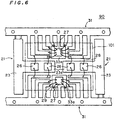
- Fig. 6 shows a semiconductor device described in Japanese Patent Laying-Open Gazette No. 5-299576.
- the semiconductor device 90 shown in Fig. 6 has a structure of storing power devices and IC-ed control devices controlling these power devices in the same package, and is called a multi-chip type semiconductor device.
- the power chips 26 and the control chips 27 are electrically connected with the external leads extending from the lead frames 31 by aluminum wires 28 and gold wires 29 respectively. It comes to that the power chips 26 and the control chips 27 are sealed with outer packaging resin 101 which is formed on a region enclosed with one-dot chain lines shown in Fig. 6.
- wire bonding In the wire bonding, reliable bonding cannot be performed unless the material for the wires and the material for the parts to which these wires are connected are properly combined with each other.
- At least connecting portions must be of nickel in the external leads connecting the aluminum wires 28, and at least connecting portions must be of silver in the external leads connecting the gold wires 29. Since the lead frames 31 are made of copper in general, nickel plating and silver plating have been performed on the parts to which the aluminum wires 28 and the gold wires 29 are connected.
- a copper plate serving as the material is worked by punching for forming a lead frame and thereafter covering a part not to be plated with a mask for performing plating only on an opening part, while the shape of the mask is complicated and a step of sticking the mask to the lead frame is troublesome, and hence there have been such problems that workability of assembly is inferior and the assembly cost is high.
- the power chip mounting regions 23a and the control chip mounting regions 33a have been in structures connected to the lead frames 31 in single directions. Therefore, the same are in cantilevered states and readily deformed if excess force is applied, and hence there have been such problems that bonding operations for the power chips 26 and the control chips 27 and an operation for transporting the lead frames 31 after wire-bonding the aluminum wires 28 and the gold wires 29 are not easy, operability is inferior and the assembly cost is high.
- enlargement of an IPM progresses, and particularly power chips enlarge and the weight also tends to get heavy. In such circumstances, it prompts the aforementioned problems that the power chip mounting regions and the control chip mounting regions, particularly the power chip mounting regions are in cantilevered structures, and hence becomes an important subject.
- the power chip mounting regions and the control chip mounting regions have been in cantilevered states, and hence there have been such problems that workability of assembly is inferior and the assembly cost is high.
- the present invention aims at solving the aforementioned problems, and providing a semiconductor device which is excellent in workability of assembly and reduces the assembly cost.
- a first aspect of the semiconductor device comprises a lead frame, a power device and a control device controlling the said power device, arranged on the said lead frame, the said power device is arranged in a first region on the said lead frame, the said control device is arranged in a second region on the said lead frame, the said first region and the said second region are divided without being intermixed with each other, the said power device is electrically connected with the said lead frame in the said first region through a first wire, the said control device is electrically connected with the said lead frame in the said second region through a second wire which is thinner than the said first wire, and the said lead frame is such that at least a region to which the said first wire is connected is a striped first plating region subjected to plating of a first material with a constant width along a prescribed direction of the said lead frame and at least a region to which the said second wire is connected is a striped second plating region subjected to plating of a second material with a constant width along the said prescribed direction of
- formation of the striped plating regions becomes possible by dividing the first region and the second region without intermixing the same with each other, for forming the striped first plating region at least on the region of the lead frame to which the first wire is connected and forming the striped second plating region at least on the region to which the second wire is connected, whereby spot plating causing reduction of workability and increase of the assembly cost becomes unnecessary in case of connecting the first wire and the second wire, and a semiconductor device which is excellent in workability of assembly and reduces the assembly cost can be obtained.
- a second aspect of the semiconductor device according to the present invention is such that the said lead frame is an integrated lead frame formed by applying a prescribed lead pattern on plates of the same thickness and the same material.
- the integrated lead frame is employed, whereby a semiconductor device which is easy in assembly operation and reduces the assembly cost can be obtained.
- a third aspect of the semiconductor device according to the present invention is such that the said first and second plating regions are formed before formation of the said prescribed lead pattern.
- the shapes of masks are simple and sticking of the masks is easy while plating is performed over a wide range by applying striped masks over the entire region of a roll material and forming prescribed striped plating regions, whereby workability is also excellent and the cost can be lowered.
- a fourth aspect of the semiconductor device according to the present invention is such that the said lead frame comprises an intermediate lead which is independent of a lead performing electrical connection between the said power device and the said control device and the device exterior, and the said intermediate lead serves as a path through which another end of the said first wire whose one end is connected to the said control device and another end of the said second wire whose one end is connected to the said power device are connected with each other for electrically connecting the control device and the power device with each other.
- the length of the first wire can be shortened by comprising the intermediate lead if the intermediate lead is provided to form a bypass path for avoiding arrangement of the first wire over a long distance, whereby workability of wire bonding becomes excellent.
- the intermediate lead is formed to avoid overhead crossing of the first wire, contact of the first wire by overhead crossing can be prevented and defective products can be reduced, while workability of wire bonding becomes excellent.
- a fifth aspect of the semiconductor device according to the present invention is such that the said lead frame comprises at least one power device die pad mounting the said power device and at least one control device die pad mounting the said control device, and the said at least one power device die pad and at least one said control device die pad further comprise suspension leads connecting the said at least one power device die pad and at least one said control device die pad to the said lead frame and supporting the same in addition to leads originally comprised for connecting the respective ones and the said lead frame.
- At least one power device die pad and at least one control device die pad are supported by the originally comprised leads and the suspension leads, whereby support strength for at least one power device die pad and at least one control device die pad increases, deflection is prevented in case of mounting the power device and the control device, bonding operations for the power device and the control device and a transport operation after wire bonding of the first and second wires become easy, and improvement of the workability and reduction of the assembly cost can be achieved.
- a sixth aspect of the semiconductor device according to the present invention is such that the said lead frame comprises four frames defining a rectangular region, the said at least one power device die pad is a plurality of power device die pads which are arranged in a line, and a power device die pad positioned on an end portion among the said plurality of power device die pads is connected to three among the said four frames by the said originally comprised leads and the said suspension leads.
- the sixth aspect of the inventive semiconductor device it comes to that it is supported by the lead frame in three directions as to the power device die pad positioned on the end portion among the plurality of power device die pads, whereby support strength increases, and deflection can be prevented by structuring the device to mount a plurality of power devices or mounting the largest power device on the power device die pad, for example.
- Fig. 1 is a diagram typically showing first and second characteristic parts according to the present invention.
- Fig. 2 is a diagram typically showing a third characteristic part according to the present invention.
- Fig. 3 is a diagram illustrating the structure of an IPM including the first and third characteristic parts according to the present invention.
- Fig. 4 is a diagram showing a concrete application example of the first characteristic part according to the present invention.
- Fig. 5 is a diagram showing the second characteristic part according to the present invention, a concrete application example.
- Fig. 6 is a diagram showing the structure of a conventional semiconductor device.
- IPM Intelligent Power Module
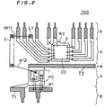
- Fig. 1 typically shows first and second characteristic parts of the IPM 100.
- Fig. 1 shows a state of fixing a power device PD and a control device CD to a lead frame 10 forming the IPM 100 by die bonding and performing wire bonding of aluminum wires W1 (first wires) and gold wires W2 (second wires).
- the lead frame 10 has a power device die pad 1 and a control device die pad 2, the power device PD is mounted on the power device die pad 1, and the control device CD is mounted on the control device die pad 2.
- the power device die pad 1 and the control device die pad 2 are arranged on single sides of the lead frame 10 respectively. Namely, the power device die pad 1 is provided on a slightly lower side with reference to the plane center, and the control device die pad 2 is provided on a slightly upper side with reference to the plane center in Fig. 1.
- the power device PD is electrically connected with a prescribed portion on the lead frame 10 through the aluminum wires W1
- the control device CD is electrically connected with a prescribed portion on the lead frame 10 through the gold wires W2, and packaging is completed.
- the device is so structured that the regions (first regions) where the aluminum wires W1 are arranged and the region (second region) where the gold wires W2 are arranged are not intermixed with each other.
- silver plating is stripedly performed along overall regions in the region where the gold wires W2 are arranged and a region where the power device die pad 1 is arranged to define silver plating regions A (second plating regions), as the first characteristic part.
- nickel plating is stripedly performed along the overall regions in the regions where the aluminum wires W1 are arranged, to define nickel plating regions B (first plating regions).
- the power device die pad 1 is connected with the lead frame 10 in two directions in Fig. 1.
- the power device die pad 1 has a rectangular shape, and its one side is connected to a tie bar T1 of the lead frame 10, while another side is connected to a tie bar T2.
- the tie bar T2 is illustrated as being provided at a central portion of the lead frame 10, while the same is not structured in this way in practice, but this typically shows that the power device die pad 1 is connected to a tie bar which is independent of the tie bar T1.
- suspension leads 43, 44, 46 and 48 in Fig. 5 described later correspond to this.
- the lead frame 10 is so formed that the regions where the aluminum wires W1 are arranged and the region where the gold wires W2 are arranged are not intermixed with each other and the gold wires W2 and the aluminum wires W1 are connected to the striped silver plating region A and the nickel plating regions B, whereby spot plating causing reduction of workability and increase of the assembly cost becomes unnecessary.
- the device is brought into the structure of connecting the power device die pad 1 with the lead frame 10 in two directions, whereby support strength for the power device die pad 1 increases, deflection is prevented in case of mounting the power device PD, a bonding operation for the power device WD and a transport operation after wire-bonding the aluminum wires W1 and the gold wires W2 become easy, and improvement of the workability and reduction of the assembly cost can be achieved.
- Fig. 1 showing the first and second characteristic parts of the IPM 100, such a structure that the aluminum wires W1 directly connect the nickel plating regions B and the power device PD with each other has been shown.
- the length of the aluminum wire W1 connecting the nickel plating region B of a lead L1 and the power device PD is longer than the remaining aluminum wires W1.
- the aluminum wires W1 are thicker than the gold wires W2, and assuming that the diameter of the gold wires W2 is 30 ⁇ m, for example, the diameter of the aluminum wires W1 is about 300 ⁇ m.
- Fig. 2 shows a third characteristic part of the IPM 100.
- the lead frame 10 has an intermediate lead 3, and the nickel plating region B of the lead L1 and the power device PD are electrically connected with each other by the intermediate lead 3 and aluminum wires W11 and W12.
- both end portions of the intermediate lead 3 are nickel plating regions B, and the nickel plating region B of one end portion of the intermediate lead 3 and the nickel plating region B of the lead L1 are connected with each other by the aluminum wire W11, while the nickel plating region B on the other end portion of the intermediate lead 3 and the power device PD are connected with each other by the aluminum wire W12.
- the nickel plating region B of the lead L1 and the power device PD are electrically connected with each other through a bypass path former by the intermediate lead 3 and the aluminum wires W11 and W12.
- the lengths of the aluminum wires W11 and W12 may be at degrees slightly longer as compared with the remaining aluminum wires W1, and the workability of wire bonding is excellent.
- an element integrating the lead L1 and the intermediate lead 3 may be referred to as an intermediate lead. In this case, that corresponding to the aluminum wire W11 becomes unnecessary.
- the intermediate lead is not only used for reducing the lengths of the aluminum wires, but also used for avoiding overhead crossing of the aluminum wires.
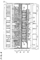
- a concrete structure of the IPM 100 comprising the aforementioned first to third characteristic parts is described with reference to Fig. 3 showing a fabrication step.
- a lead frame 10 has power device die pads 1A to 1D and a plurality of control device die pads 2 which are connected to tie bars 5, and power devices PD are mounted on the power device die pads 1A to 1D while control devices CD are mounted on the control device die pads 2 and fixed by die bonding.
- the power device die pads 1A to 1D and the control device die pads 2 are arranged on single sides of the lead frame respectively. Namely, the power device die pads 1 are arranged/formed on a slightly lower side with reference to the plane center and the control device die pads 2 are arranged/formed on a slightly upper side with reference to the plane center in Fig. 3.
- the power devices PD are electrically connected with prescribed portions on the lead frame 10 through aluminum wires W1
- the control devices CD are electrically connected with prescribed portions on the lead frame 10 through gold wires W2, and packaging is completed.
- the device is so structured that the regions (first regions) where the aluminum wires W1 are arranged and the region (second region) where the gold wires W2 are arranged are not intermixed with each other.
- intermediate leads 3A to 3D are formed in the vicinity of the control devices CD.
- the aluminum wires W1 extending from the power devices PD are connected and the gold wires W2 extending from the control devices CD are connected to the intermediate leads 3A to 3D, which serve as paths electrically connecting the power devices PD and the control devices CD with each other.
- the aluminum wires W1 shown as perpendicularly intersecting with the intermediate leads 3A and 3B are formed to extend over the intermediate leads 3A and 3B.
- Fig. 4 shows the lead frame 10 before mounting the power devices PD and the control devices CD, and the region where the gold wires W2 are arranged and the region where the power devices PD are mounted are silver plating regions A.
- the regions where the aluminum wires W1 are arranged are nickel plating regions B.
- the silver plating regions A and the nickel plating regions B are stripedly alternately provided, and both are not intermixed with each other. Formation of such striped plating is easy as compared with spot plating.
- a copper plate serving as the material for the lead frame 10 is roll-shaped at first. While this is drawn out and worked into a plate and prescribed lead patterns are formed by punching, portions subjected to silver plating and portions subjected to nickel plating are distinguished by performing striped masks on the overall region of the copper plate of the material in advance of punching, for forming the silver plating regions A and the nickel plating regions B by prescribed plating steps.
- the shapes of the masks for performing plating are simple, sticking of the masks is easy and it is possible to perform plating over a wide range, whereby the workability is also excellent and the cost can be lowered.
- Cutting, electric discharge machining, etching or the like may be used for formation of the prescribed lead patterns, in addition to punching.
- Fig. 5 shows the lead frame 10 before mounting the power devices PD and the control devices CD, hatching specifying the silver plating regions A and the nickel plating regions B is omitted and hatching is performed on the power device die pads 1A to 1D and suspension leads (fixing pins) 40 to 50 supporting these.
- the power device die pad 1A has a wide area since the same mounts three power devices PD as shown in Fig. 3. It is connected to the tie bars 5 and a frame 6 by the suspension leads 40 to 44 and supported. It comes to that the power device die pad 1A is supported in three directions, since the same is connected to the tie bar 5 on the lower side of the figure by the suspension lead 40, connected to the frame 6 on the left side of the figure by the suspension leads 41 and 42 and connected to the tie bar 5 on the upper side of the figure by the suspension leads 43 and 44.
- suspension leads are strictly leads denoted by reference numerals 41 to 44, 46, 48 and 50, and leads denoted by reference numerals 40, 45, 47 and 49 are leads which integrate the power device die pads 1A to 1D with the lead frame 10 and are originally provided for serving also as current paths.
- the power device die pad 1A can be thus supported in three directions, since the lead frame 10 is an integrated lead frame which is formed by punching plates of the same thickness and the same material.
- suspension leads cannot be formed to be connected to both tie bars and the power device die pad cannot be supported in three directions.
- the suspension leads can be connected to both of the opposite tie bars 5, whereby three-directional supporting becomes possible. If the power device die pad is only one, four-directional supporting is also possible.
- the power device die pad 1B is supported in two directions, since the same is connected to the tie bar 5 on the lower side of the figure by the suspension lead 45 and connected to the tie bar 5 on the upper side of the figure by the suspension lead 46.
- the power device die pad 1C is supported in two directions, since the same is connected to the tie bar 5 on the lower side of the figure by the suspension lead 47 and connected to the tie bar 5 on the upper side of the figure by the suspension lead 48.
- the power device die pad 1D is supported in two directions, since the same is connected to the tie bar 5 on the lower side of the figure by the suspension lead 49 and connected to the frame 6 on the right side of the figure by the suspension lead 50.
- the tie bars 5 are parts of the lead frame 10, and may be treated as frames similarly to the frames 6.
- the power device die pads 1A to 1D are supported in three directions or two directions, whereby the same are prevented from deflection in case of mounting the power devices PD, and a bonding operation for the power devices PD and a transport operation after wire bonding become easy.
- control device die pads 2 comprise the suspension leads 51 and 52 shown in Fig. 5 and are supported in two directions as to the two positioned on the endmost portions of the arrangement, the remaining control device die pads 2 are supported only in one direction.
- the control devices CD are small as compared with the power devices PD and light in weight, and hence there is no problem in particular.
Landscapes
- Lead Frames For Integrated Circuits (AREA)
- Wire Bonding (AREA)
Applications Claiming Priority (1)
| Application Number | Priority Date | Filing Date | Title |
|---|---|---|---|
| PCT/JP1996/003495 WO1998024128A1 (fr) | 1996-11-28 | 1996-11-28 | Dispositif a semi-conducteur |
Publications (3)
| Publication Number | Publication Date |
|---|---|
| EP0881680A2 true EP0881680A2 (fr) | 1998-12-02 |
| EP0881680A4 EP0881680A4 (fr) | 2000-11-29 |
| EP0881680B1 EP0881680B1 (fr) | 2008-10-01 |
Family
ID=14154167
Family Applications (1)
| Application Number | Title | Priority Date | Filing Date |
|---|---|---|---|
| EP96940146A Expired - Lifetime EP0881680B1 (fr) | 1996-11-28 | 1996-11-28 | Dispositif a semi-conducteur |
Country Status (5)
| Country | Link |
|---|---|
| US (1) | US5998856A (fr) |
| EP (1) | EP0881680B1 (fr) |
| JP (1) | JP3337224B2 (fr) |
| DE (1) | DE69637698D1 (fr) |
| WO (1) | WO1998024128A1 (fr) |
Cited By (1)
| Publication number | Priority date | Publication date | Assignee | Title |
|---|---|---|---|---|
| US9530724B2 (en) | 2010-12-13 | 2016-12-27 | Infineon Technologies Americas Corp. | Compact power quad flat no-lead (PQFN) package |
Families Citing this family (29)
| Publication number | Priority date | Publication date | Assignee | Title |
|---|---|---|---|---|
| US6184585B1 (en) * | 1997-11-13 | 2001-02-06 | International Rectifier Corp. | Co-packaged MOS-gated device and control integrated circuit |
| DE19805785C1 (de) * | 1998-02-12 | 1999-06-17 | Siemens Ag | Leistungshalbleiter-Modul mit thermischer Laststromsicherung |
| DE19912441A1 (de) * | 1999-03-19 | 2000-09-21 | Elfo Ag Sachseln Sachseln | Multi-Chip-Modul |
| KR200169860Y1 (ko) * | 1999-05-28 | 2000-02-15 | 광전자주식회사 | 전압 레귤레이터의 구조 |
| KR100322098B1 (ko) * | 1999-11-18 | 2002-02-06 | 김순택 | 2차 전지 |
| JP4037589B2 (ja) * | 2000-03-07 | 2008-01-23 | 三菱電機株式会社 | 樹脂封止形電力用半導体装置 |
| US6465875B2 (en) * | 2000-03-27 | 2002-10-15 | International Rectifier Corporation | Semiconductor device package with plural pad lead frame |
| CN1331227C (zh) * | 2001-01-11 | 2007-08-08 | 松下电器产业株式会社 | 电路板及其制造方法 |
| JP2003086756A (ja) * | 2001-09-11 | 2003-03-20 | Denso Corp | Icパッケージおよびその製造方法 |
| KR100442847B1 (ko) * | 2001-09-17 | 2004-08-02 | 페어차일드코리아반도체 주식회사 | 3차원 구조를 갖는 전력 반도체 모듈 및 그 제조방법 |
| US6900527B1 (en) * | 2001-09-19 | 2005-05-31 | Amkor Technology, Inc. | Lead-frame method and assembly for interconnecting circuits within a circuit module |
| US7105899B2 (en) * | 2002-01-17 | 2006-09-12 | Micron Technology, Inc. | Transistor structure having reduced transistor leakage attributes |
| DE10243454C5 (de) * | 2002-09-19 | 2009-10-08 | Koenig & Bauer Aktiengesellschaft | Antriebsvorrichtung einer Bearbeitungsmaschine |
| DE102006033023A1 (de) * | 2006-07-17 | 2008-01-24 | Robert Bosch Gmbh | Halbleiteranordnung und entsprechendes Herstellungsverfahren |
| JP5011879B2 (ja) * | 2006-08-09 | 2012-08-29 | サンケン電気株式会社 | 半導体装置及びリードフレーム組立体の製法 |
| US7902655B1 (en) | 2006-08-15 | 2011-03-08 | Marvell International Ltd. | Multichip package leadframe including electrical bussing |
| US7466016B2 (en) * | 2007-04-07 | 2008-12-16 | Kevin Yang | Bent lead transistor |
| JP2011243839A (ja) * | 2010-05-20 | 2011-12-01 | Mitsubishi Electric Corp | 電力用半導体装置 |
| US9443795B2 (en) | 2010-12-13 | 2016-09-13 | Infineon Technologies Americas Corp. | Power quad flat no-lead (PQFN) package having bootstrap diodes on a common integrated circuit (IC) |
| US9355995B2 (en) | 2010-12-13 | 2016-05-31 | Infineon Technologies Americas Corp. | Semiconductor packages utilizing leadframe panels with grooves in connecting bars |
| US9449957B2 (en) | 2010-12-13 | 2016-09-20 | Infineon Technologies Americas Corp. | Control and driver circuits on a power quad flat no-lead (PQFN) leadframe |
| US9362215B2 (en) | 2010-12-13 | 2016-06-07 | Infineon Technologies Americas Corp. | Power quad flat no-lead (PQFN) semiconductor package with leadframe islands for multi-phase power inverter |
| US9711437B2 (en) | 2010-12-13 | 2017-07-18 | Infineon Technologies Americas Corp. | Semiconductor package having multi-phase power inverter with internal temperature sensor |
| US9659845B2 (en) | 2010-12-13 | 2017-05-23 | Infineon Technologies Americas Corp. | Power quad flat no-lead (PQFN) package in a single shunt inverter circuit |
| US9620954B2 (en) | 2010-12-13 | 2017-04-11 | Infineon Technologies Americas Corp. | Semiconductor package having an over-temperature protection circuit utilizing multiple temperature threshold values |
| US9324646B2 (en) | 2010-12-13 | 2016-04-26 | Infineon Technologies America Corp. | Open source power quad flat no-lead (PQFN) package |
| US9524928B2 (en) | 2010-12-13 | 2016-12-20 | Infineon Technologies Americas Corp. | Power quad flat no-lead (PQFN) package having control and driver circuits |
| JP5251991B2 (ja) * | 2011-01-14 | 2013-07-31 | トヨタ自動車株式会社 | 半導体モジュール |
| JP6408038B2 (ja) * | 2017-01-10 | 2018-10-17 | ルネサスエレクトロニクス株式会社 | 半導体装置の製造方法 |
Family Cites Families (17)
| Publication number | Priority date | Publication date | Assignee | Title |
|---|---|---|---|---|
| JPH0357259A (ja) * | 1989-07-26 | 1991-03-12 | Hitachi Ltd | 半導体装置 |
| JPH03188661A (ja) * | 1989-12-18 | 1991-08-16 | Toshiba Corp | 樹脂封止型半導体装置 |
| JPH03274755A (ja) * | 1990-03-26 | 1991-12-05 | Hitachi Ltd | 樹脂封止半導体装置とその製造方法 |
| US5049973A (en) * | 1990-06-26 | 1991-09-17 | Harris Semiconductor Patents, Inc. | Heat sink and multi mount pad lead frame package and method for electrically isolating semiconductor die(s) |
| JPH0529539A (ja) * | 1991-07-17 | 1993-02-05 | Matsushita Electric Works Ltd | マルチチツプモジユール |
| JPH05206365A (ja) * | 1992-01-30 | 1993-08-13 | Fuji Electric Co Ltd | 半導体装置およびその組立用リードフレーム |
| JP2708320B2 (ja) * | 1992-04-17 | 1998-02-04 | 三菱電機株式会社 | マルチチップ型半導体装置及びその製造方法 |
| JPH069152A (ja) * | 1992-06-24 | 1994-01-18 | Hitachi Cable Ltd | 連続自動ボビン巻き用上端末調整装置 |
| JPH06132457A (ja) * | 1992-10-15 | 1994-05-13 | Mitsubishi Electric Corp | 半導体装置およびその製造方法 |
| JPH06277775A (ja) * | 1993-03-25 | 1994-10-04 | Kobe Steel Ltd | Agめっき層を有する材料の製造方法 |
| JPH07101729B2 (ja) * | 1993-03-26 | 1995-11-01 | 日本電気株式会社 | マルチチップ半導体装置およびその製造方法 |
| JP2701712B2 (ja) * | 1993-11-11 | 1998-01-21 | 日本電気株式会社 | 半導体装置 |
| JPH07161905A (ja) * | 1993-12-13 | 1995-06-23 | Hitachi Cable Ltd | 半導体装置用リードフレーム及びその製造方法 |
| JP3325697B2 (ja) * | 1994-01-20 | 2002-09-17 | 三菱電機株式会社 | パワーデバイスの制御装置およびモータの駆動制御装置 |
| US5530284A (en) * | 1995-03-06 | 1996-06-25 | Motorola, Inc. | Semiconductor leadframe structure compatible with differing bond wire materials |
| JP3429921B2 (ja) * | 1995-10-26 | 2003-07-28 | 三菱電機株式会社 | 半導体装置 |
| US5767567A (en) * | 1996-09-10 | 1998-06-16 | Magemos Corporation | Design of device layout for integration with power mosfet packaging to achieve better lead wire connections and lower on resistance |
-
1996
- 1996-11-28 WO PCT/JP1996/003495 patent/WO1998024128A1/fr not_active Ceased
- 1996-11-28 EP EP96940146A patent/EP0881680B1/fr not_active Expired - Lifetime
- 1996-11-28 JP JP52236598A patent/JP3337224B2/ja not_active Expired - Lifetime
- 1996-11-28 US US09/117,172 patent/US5998856A/en not_active Expired - Lifetime
- 1996-11-28 DE DE69637698T patent/DE69637698D1/de not_active Expired - Lifetime
Cited By (2)
| Publication number | Priority date | Publication date | Assignee | Title |
|---|---|---|---|---|
| US9530724B2 (en) | 2010-12-13 | 2016-12-27 | Infineon Technologies Americas Corp. | Compact power quad flat no-lead (PQFN) package |
| EP2463904B1 (fr) * | 2010-12-13 | 2019-02-27 | Infineon Technologies Americas Corp. | Paquet semi-conducteur sans fil plat quadruple d'alimentation pour module multi-puces utilisant une grille de connexion pour interconnexions électriques |
Also Published As
| Publication number | Publication date |
|---|---|
| EP0881680A4 (fr) | 2000-11-29 |
| WO1998024128A1 (fr) | 1998-06-04 |
| DE69637698D1 (de) | 2008-11-13 |
| US5998856A (en) | 1999-12-07 |
| EP0881680B1 (fr) | 2008-10-01 |
| JP3337224B2 (ja) | 2002-10-21 |
Similar Documents
| Publication | Publication Date | Title |
|---|---|---|
| US5998856A (en) | Semiconductor device | |
| EP0354696B1 (fr) | Dispositif semi-conducteur comprenant un cadre conducteur | |
| JPWO1998024128A1 (ja) | 半導体装置 | |
| US6570244B1 (en) | Multi-part lead frame with dissimilar materials | |
| US5723899A (en) | Semiconductor lead frame having connection bar and guide rings | |
| US6558980B2 (en) | Plastic molded type semiconductor device and fabrication process thereof | |
| US6762079B2 (en) | Methods for fabricating dual loc semiconductor die assembly employing floating lead finger structure | |
| US20090014848A1 (en) | Mixed Wire Semiconductor Lead Frame Package | |
| KR0144164B1 (ko) | 엘오씨 반도체 패키지 및 반도체 장치를 패키징하는 방법 | |
| US6677665B2 (en) | Dual-die integrated circuit package | |
| US5926695A (en) | Lead frame incorporating material flow diverters | |
| KR950000205B1 (ko) | 리이드 프레임 및 이를 사용한 반도체 장치 | |
| EP1065712A1 (fr) | Méthode de soudure de fil dans un dispositif semiconducteur | |
| US7541664B2 (en) | Lead frame and semiconductor device having the lead frame | |
| JP2765542B2 (ja) | 樹脂封止型半導体装置 | |
| US5408127A (en) | Method of and arrangement for preventing bonding wire shorts with certain integrated circuit components | |
| US6943456B2 (en) | Plastic molded type semiconductor device and fabrication process thereof | |
| JP2924957B2 (ja) | 樹脂封止型半導体装置 | |
| JPH1140563A (ja) | 半導体装置およびその電気特性変更方法 | |
| JPH04317363A (ja) | ダイパッドレス樹脂封止型半導体装置とその製造方法 | |
| KR100244254B1 (ko) | 리드 프레임 및 이를 이용한 반도체 패키지 | |
| KR200331874Y1 (ko) | 반도체의다핀형태패키지 | |
| KR970005721B1 (ko) | 반도체 패키지용 리드 프레임 | |
| KR100523914B1 (ko) | 골드리본이 프리-디자인된 와이어 본딩용 테이프 및 이를 이용한 와이어 본딩 방법 | |
| JPH02202046A (ja) | リードフレームおよびこれを用いた半導体装置の製造方法 |
Legal Events
| Date | Code | Title | Description |
|---|---|---|---|
| PUAI | Public reference made under article 153(3) epc to a published international application that has entered the european phase |
Free format text: ORIGINAL CODE: 0009012 |
|
| 17P | Request for examination filed |
Effective date: 19980728 |
|
| AK | Designated contracting states |
Kind code of ref document: A2 Designated state(s): DE FR GB |
|
| A4 | Supplementary search report drawn up and despatched |
Effective date: 20001018 |
|
| AK | Designated contracting states |
Kind code of ref document: A4 Designated state(s): DE FR GB |
|
| RIC1 | Information provided on ipc code assigned before grant |
Free format text: 7H 01L 25/04 A, 7H 01L 23/495 B |
|
| RAP1 | Party data changed (applicant data changed or rights of an application transferred) |
Owner name: MITSUBISHI DENKI KABUSHIKI KAISHA |
|
| GRAP | Despatch of communication of intention to grant a patent |
Free format text: ORIGINAL CODE: EPIDOSNIGR1 |
|
| GRAS | Grant fee paid |
Free format text: ORIGINAL CODE: EPIDOSNIGR3 |
|
| GRAA | (expected) grant |
Free format text: ORIGINAL CODE: 0009210 |
|
| AK | Designated contracting states |
Kind code of ref document: B1 Designated state(s): DE FR GB |
|
| REG | Reference to a national code |
Ref country code: GB Ref legal event code: FG4D |
|
| REF | Corresponds to: |
Ref document number: 69637698 Country of ref document: DE Date of ref document: 20081113 Kind code of ref document: P |
|
| PLBE | No opposition filed within time limit |
Free format text: ORIGINAL CODE: 0009261 |
|
| STAA | Information on the status of an ep patent application or granted ep patent |
Free format text: STATUS: NO OPPOSITION FILED WITHIN TIME LIMIT |
|
| 26N | No opposition filed |
Effective date: 20090702 |
|
| REG | Reference to a national code |
Ref country code: GB Ref legal event code: 746 Effective date: 20110513 |
|
| REG | Reference to a national code |
Ref country code: DE Ref legal event code: R084 Ref document number: 69637698 Country of ref document: DE Effective date: 20110506 Ref country code: DE Ref legal event code: R084 Ref document number: 69637698 Country of ref document: DE Effective date: 20110706 |
|
| REG | Reference to a national code |
Ref country code: FR Ref legal event code: PLFP Year of fee payment: 20 |
|
| PGFP | Annual fee paid to national office [announced via postgrant information from national office to epo] |
Ref country code: DE Payment date: 20151125 Year of fee payment: 20 Ref country code: GB Payment date: 20151125 Year of fee payment: 20 |
|
| PGFP | Annual fee paid to national office [announced via postgrant information from national office to epo] |
Ref country code: FR Payment date: 20151008 Year of fee payment: 20 |
|
| REG | Reference to a national code |
Ref country code: DE Ref legal event code: R071 Ref document number: 69637698 Country of ref document: DE |
|
| REG | Reference to a national code |
Ref country code: GB Ref legal event code: PE20 Expiry date: 20161127 |
|
| PG25 | Lapsed in a contracting state [announced via postgrant information from national office to epo] |
Ref country code: GB Free format text: LAPSE BECAUSE OF EXPIRATION OF PROTECTION Effective date: 20161127 |