EP0893819B1 - Dispositif et méthode pour le lavage de substrat - Google Patents
Dispositif et méthode pour le lavage de substrat Download PDFInfo
- Publication number
- EP0893819B1 EP0893819B1 EP98113546A EP98113546A EP0893819B1 EP 0893819 B1 EP0893819 B1 EP 0893819B1 EP 98113546 A EP98113546 A EP 98113546A EP 98113546 A EP98113546 A EP 98113546A EP 0893819 B1 EP0893819 B1 EP 0893819B1
- Authority
- EP
- European Patent Office
- Prior art keywords
- washing
- substrate
- brush
- wafer
- spin chuck
- Prior art date
- Legal status (The legal status is an assumption and is not a legal conclusion. Google has not performed a legal analysis and makes no representation as to the accuracy of the status listed.)
- Expired - Lifetime
Links
Images






Classifications
-
- H—ELECTRICITY
- H10—SEMICONDUCTOR DEVICES; ELECTRIC SOLID-STATE DEVICES NOT OTHERWISE PROVIDED FOR
- H10P—GENERIC PROCESSES OR APPARATUS FOR THE MANUFACTURE OR TREATMENT OF DEVICES COVERED BY CLASS H10
- H10P70/00—Cleaning of wafers, substrates or parts of devices
- H10P70/10—Cleaning before device manufacture, i.e. Begin-Of-Line process
- H10P70/15—Cleaning before device manufacture, i.e. Begin-Of-Line process by wet cleaning only
-
- B—PERFORMING OPERATIONS; TRANSPORTING
- B08—CLEANING
- B08B—CLEANING IN GENERAL; PREVENTION OF FOULING IN GENERAL
- B08B1/00—Cleaning by methods involving the use of tools
- B08B1/30—Cleaning by methods involving the use of tools by movement of cleaning members over a surface
- B08B1/32—Cleaning by methods involving the use of tools by movement of cleaning members over a surface using rotary cleaning members
-
- B—PERFORMING OPERATIONS; TRANSPORTING
- B08—CLEANING
- B08B—CLEANING IN GENERAL; PREVENTION OF FOULING IN GENERAL
- B08B1/00—Cleaning by methods involving the use of tools
- B08B1/30—Cleaning by methods involving the use of tools by movement of cleaning members over a surface
- B08B1/32—Cleaning by methods involving the use of tools by movement of cleaning members over a surface using rotary cleaning members
- B08B1/36—Cleaning by methods involving the use of tools by movement of cleaning members over a surface using rotary cleaning members rotating about an axis orthogonal to the surface
-
- B—PERFORMING OPERATIONS; TRANSPORTING
- B08—CLEANING
- B08B—CLEANING IN GENERAL; PREVENTION OF FOULING IN GENERAL
- B08B1/00—Cleaning by methods involving the use of tools
- B08B1/50—Cleaning by methods involving the use of tools involving cleaning of the cleaning members
- B08B1/52—Cleaning by methods involving the use of tools involving cleaning of the cleaning members using fluids
-
- B—PERFORMING OPERATIONS; TRANSPORTING
- B08—CLEANING
- B08B—CLEANING IN GENERAL; PREVENTION OF FOULING IN GENERAL
- B08B3/00—Cleaning by methods involving the use or presence of liquid or steam
- B08B3/02—Cleaning by the force of jets or sprays
-
- H—ELECTRICITY
- H10—SEMICONDUCTOR DEVICES; ELECTRIC SOLID-STATE DEVICES NOT OTHERWISE PROVIDED FOR
- H10P—GENERIC PROCESSES OR APPARATUS FOR THE MANUFACTURE OR TREATMENT OF DEVICES COVERED BY CLASS H10
- H10P70/00—Cleaning of wafers, substrates or parts of devices
- H10P70/60—Cleaning only by mechanical processes
-
- H—ELECTRICITY
- H10—SEMICONDUCTOR DEVICES; ELECTRIC SOLID-STATE DEVICES NOT OTHERWISE PROVIDED FOR
- H10P—GENERIC PROCESSES OR APPARATUS FOR THE MANUFACTURE OR TREATMENT OF DEVICES COVERED BY CLASS H10
- H10P72/00—Handling or holding of wafers, substrates or devices during manufacture or treatment thereof
- H10P72/04—Apparatus for manufacture or treatment
- H10P72/0402—Apparatus for fluid treatment
- H10P72/0406—Apparatus for fluid treatment for cleaning followed by drying, rinsing, stripping, blasting or the like
- H10P72/0411—Apparatus for fluid treatment for cleaning followed by drying, rinsing, stripping, blasting or the like for wet cleaning or washing
- H10P72/0412—Apparatus for fluid treatment for cleaning followed by drying, rinsing, stripping, blasting or the like for wet cleaning or washing using mainly scrubbing means, e.g. brushes
-
- H—ELECTRICITY
- H10—SEMICONDUCTOR DEVICES; ELECTRIC SOLID-STATE DEVICES NOT OTHERWISE PROVIDED FOR
- H10P—GENERIC PROCESSES OR APPARATUS FOR THE MANUFACTURE OR TREATMENT OF DEVICES COVERED BY CLASS H10
- H10P72/00—Handling or holding of wafers, substrates or devices during manufacture or treatment thereof
- H10P72/04—Apparatus for manufacture or treatment
- H10P72/0402—Apparatus for fluid treatment
- H10P72/0406—Apparatus for fluid treatment for cleaning followed by drying, rinsing, stripping, blasting or the like
- H10P72/0411—Apparatus for fluid treatment for cleaning followed by drying, rinsing, stripping, blasting or the like for wet cleaning or washing
- H10P72/0414—Apparatus for fluid treatment for cleaning followed by drying, rinsing, stripping, blasting or the like for wet cleaning or washing using mainly spraying means, e.g. nozzles
-
- H—ELECTRICITY
- H10—SEMICONDUCTOR DEVICES; ELECTRIC SOLID-STATE DEVICES NOT OTHERWISE PROVIDED FOR
- H10P—GENERIC PROCESSES OR APPARATUS FOR THE MANUFACTURE OR TREATMENT OF DEVICES COVERED BY CLASS H10
- H10P72/00—Handling or holding of wafers, substrates or devices during manufacture or treatment thereof
- H10P72/06—Apparatus for monitoring, sorting, marking, testing or measuring
-
- H—ELECTRICITY
- H10—SEMICONDUCTOR DEVICES; ELECTRIC SOLID-STATE DEVICES NOT OTHERWISE PROVIDED FOR
- H10P—GENERIC PROCESSES OR APPARATUS FOR THE MANUFACTURE OR TREATMENT OF DEVICES COVERED BY CLASS H10
- H10P72/00—Handling or holding of wafers, substrates or devices during manufacture or treatment thereof
- H10P72/70—Handling or holding of wafers, substrates or devices during manufacture or treatment thereof for supporting or gripping
- H10P72/76—Handling or holding of wafers, substrates or devices during manufacture or treatment thereof for supporting or gripping using mechanical means, e.g. clamps or pinches
- H10P72/7604—Handling or holding of wafers, substrates or devices during manufacture or treatment thereof for supporting or gripping using mechanical means, e.g. clamps or pinches the wafers being placed on a susceptor, stage or support
- H10P72/7624—Handling or holding of wafers, substrates or devices during manufacture or treatment thereof for supporting or gripping using mechanical means, e.g. clamps or pinches the wafers being placed on a susceptor, stage or support characterised by the mechanical construction of the susceptor, stage or support
-
- Y—GENERAL TAGGING OF NEW TECHNOLOGICAL DEVELOPMENTS; GENERAL TAGGING OF CROSS-SECTIONAL TECHNOLOGIES SPANNING OVER SEVERAL SECTIONS OF THE IPC; TECHNICAL SUBJECTS COVERED BY FORMER USPC CROSS-REFERENCE ART COLLECTIONS [XRACs] AND DIGESTS
- Y10—TECHNICAL SUBJECTS COVERED BY FORMER USPC
- Y10S—TECHNICAL SUBJECTS COVERED BY FORMER USPC CROSS-REFERENCE ART COLLECTIONS [XRACs] AND DIGESTS
- Y10S134/00—Cleaning and liquid contact with solids
- Y10S134/902—Semiconductor wafer
Definitions
- the present invention relates to an apparatus and method for washing a substrate for cleansing a surface of a substrate such as a semiconductor wafer or an LCD substrate.
- a surface of a semiconductor wafer is strictly required to be maintained at a high cleanliness.
- a surface of a wafer is washed every time the wafer is subjected to any treatment or both before and after the treating process.
- the photolithography step it is absolutely necessary to wash the surface of the wafer.
- the washing treatment of the wafer surface is carried out by a scrub-washing apparatus disclosed in, for example, Japanese Patent Disclosure (Kokai) No. 57-102024 or Japanese Patent Disclosure No. 62-259447.
- a rotary brush is brought into contact with a wafer surface while applying a washing liquid to the wafer surface.
- the rotary brush is moved at a predetermined speed along the wafer surface from a central portion toward a peripheral portion of the wafer so as to remove contaminants attached to the wafer surface.
- the Japanese patent application 08-243518 discloses a rotary substrate washer comprising washing means for applying physical force to contaminants present on a surface of the substrate, a supporting arm, and control means for controlling the operation of the washing means to control the physical force acting on the contaminants. Therefore, a pressure sensor is provided for detecting the pressure of the washing means to a substrate. The pressure sensor and a pressure setter are connected to a controller. The pressure setter is operated prior to cleaning of a wafer to input and appropriate cleaning pressure according to the type of layer formed on the wafer (e.g. aluminum, oxide, nitride, polysilicon, patterned or bare silicon) and the property or type of contaminant adhering the wafer.
- the type of layer formed on the wafer e.g. aluminum, oxide, nitride, polysilicon, patterned or bare silicon
- the contaminants attached to the wafer surface are not necessarily distributed uniformly over the entire wafer surface. For example, these contaminants are concentrated in a central portion or in a region of the peripheral portion of the wafer. Therefore, the contaminants tend to remain in the heavily stained portion even after the washing treatment. If the washing time is simply increased in an attempt to overcome this difficulty, the region of a high cleanliness tends to be lowered in cleanliness.
- the decrease in cleanliness of the originally dean region is considered to be derived from the fact that the rotary brush itself generates contaminants in the level of cleanliness required in the manufacturing process of a semiconductor device.
- An object of the present invention is to provide an apparatus for washing a substrate, which permits washing the entire surface of a substrate uniformly and at a high cleanliness.
- Another object is to provide a method of washing a substrate, which permits washing the substrate in a short time depending on the degree of stains on the substrate surface and which also permits increasing the through-put of the washing treatment.
- an apparatus for washing a substrate comprising:
- Said apparatus further comprises means adapted to supply distribution data of the distribution of contaminants on the surface of the substrate; and control means in communication with said means adapted to supply distribution data, said control means adapted to control the operation of at least one of the washing means, the spin chuck and the arm driving mechanism so as to control the physical force acting on the contaminants present on the surface of the substrate in accordance with the distribution data received from said means adapted to supply distribution data.
- the washing means used in the present invention is not limited to a brush for the scrub-washing.
- the washing means an ultrasonic washer (i. e., a megasonic washing utilizing ultrasonic wave of several megahertz), in which an ultrasonic wave is applied to the washing liquid for washing the substrate surface, or a water jet washer in which a water jet is applied to the substrate surface for the washing purpose.
- a method of washing a substrate comprising the steps of:
- the washing conditions are controlled depending on the local state of stains on the washing surface of the substrate. For example, where a large amount of contaminants are present in a central portion of the wafer surface, the moving speed of the brush (or ultrasonic washing nozzle) is lowered in the central portion of the wafer.
- the moving speed of the brush is lowered in the peripheral portion of the wafer.
- the brush is moved at a high speed in a clean portion where the amount of contaminants is small, with the result that the contaminants generated from the brush itself are not attached to the clean portion. It follows that the washing surface of the substrate can be washed uniformly and at a high cleanliness.
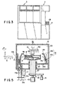
- FIGS. 1 to 3 collectively show a wafer washing system 1.
- the wafer washing system 1 comprises a cassette section 2 and a process section 3.
- Four projections 4a are mounted to a cassette table 4 in the cassette section 2. If a cassette CR is mounted on any of the projections 4a, the cassette CR is automatically arranged in a desired position.
- a transfer path 5a is formed along the cassette table 4.
- a sub-arm mechanism 5 is moved along the transfer path 5a so as to obtain access to each of the cassettes CR.
- the sub-arm mechanism 5 comprises a wafer holder, a back-and-forth driving mechanism for moving the wafer holder back and forth, an X-axis driving mechanism for moving the wafer holder in the X-axis direction, a Z-axis driving mechanism for moving the wafer holder in the Z-axis direction, and a ⁇ -swinging mechanism for swinging the wafer holder about the Z-axis.
- the process section 3 comprises a main arm mechanism 6, five washing units 7A to 7E, and an inspecting unit 8.
- the main arm mechanism 6 comprises a back-and-forth driving mechanism for moving the wafer holder back and forth, a Y-axis driving mechanism for moving the wafer holder in the Y-axis direction, a Z-axis driving mechanism for moving the wafer holder in the Z-axis direction, and a ⁇ -swinging mechanism for swinging the wafer holder about the Z-axis.
- the main arm mechanism 6 Upon receipt of the wafer W from the sub-arm mechanism 5, the main arm mechanism 6 is moved along a central transfer path 6a so as to deliver the wafer W into each of the washing units 7A to 7E and the inspecting unit 8.
- the washing units 7A, 7B and 7C are arranged side by side on one side of the central transfer path 6a.
- the two washing units 7D, 7E and the inspecting unit 8 are arranged side by side on the other side of the central transfer path 6a
- Each of the first and second washing units 7A and 7B is equipped with a megasonic washing mechanism in which an ultrasonic wave of several megahertz is applied to a washing liquid (pure water) while supplying the washing liquid to the wafer.
- the third washing unit 7C is equipped with a high pressure water jet mechanism in which a high pressure jet water is spurted against the wafer for washing the wafer surface.
- the fourth washing unit 7D is equipped with a one surface scrub-washing mechanism in which an upper surface of the wafer is washed with a brush while supplying a washing liquid to the wafer W.
- the fifth washing unit 7E is equipped with a both surface scrub-washing mechanism in which both upper and lower surfaces of the wafer W are washed with brushes while supplying a washing liquid to both surfaces of the wafer.
- the inspecting unit 8 is equipped with a turntable (not shown) for holding and rotating the wafer W and with sensors 28, 29 (see FIG. 10).
- the surface of the wafer disposed on the turntable is irradiated with a laser light beam for allowing the sensors 28, 29 to detect contaminants present on the wafer surface.
- a laser light emitted from the light emitting section 28 is applied to the surface of the wafer W which is kept rotated, and the reflected light is detected by the light receiving section 29.
- a signal denoting the detection is supplied to a control device 80.
- Data showing the relationship between the amount of the detected laser light and the surface state of the wafer W (i.e., distribution and size of contaminants), which are measured in advance, are stored in a memory of the control device 80 as initially set data.
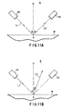
- the light emitting section 28 and the light receiving section 29 are arranged within the inspecting unit 8 in symmetry with respect to a normal line RH.
- each of the emitted light L1 and the reflected light L2 forms an angle ⁇ with the normal line RH in the case where contaminants are not present in a measuring point R.
- the laser light L1 emitted from the light emitting section 28 to form an angle ⁇ with the normal line RH is regularly reflected at the measuring point R, with the result that the reflected light L2 forming an angle ⁇ with the normal line RH is detected by the light receiving section 29.
- the emitted light L1 is irregularly reflected at the measuring point R, with the result that the reflected light L3 forms an angle ⁇ differing from the angle ⁇ , as shown in FIG. 11B.
- the reflected light L3 fails to be detected by the light receiving section 29. In this fashion, the distribution of the contaminants is measured over the entire surface of the wafer W, and the result of the measurement is supplied to the control device 80.
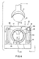
- the fifth washing unit 7E comprises a process chamber 12a for processing the semiconductor wafer W.
- the process chamber 12a is provided with an opening 12b through which the wafer W is transferred.
- the opening 12b is opened or closed by a shutter 13.
- the main arm mechanism 6 serves to load or unload the wafer W into and out of the process chamber 12a through the opening 12b.
- a spin chuck 9 Arranged within the process chamber 12a are a spin chuck 9, an upper brush mechanism 10, a cup 14, a jet water spurting nozzle 15, a rinsing nozzle 16 and a lower brush mechanism 40.
- the spin chuck 9 is equipped with a rotary driving mechanism 30, a hollow shaft 37, a liquid receiving section 32 and a wafer holding section 33.
- the rotary driving mechanism 30 comprises a motor 19, a driving pulley 19a, a driven pulley 38 and a belt 39 which is stretch between the driving pulley 19a and the hollow shaft 38.
- the hollow shaft 38 is rotatably supported by a frame 35 via a bearing 36, and the upper end portion of the hollow shaft 38 is joined to the liquid receiving section 32.
- a wafer holding section 33 is joined to the upper portion of the liquid receiving section 32.
- the wafer holding section 33 comprises three movable holding members 70 serving to press radially inward the peripheral edge portion of the wafer W and six stationary holding members 71 defining the peripheral edge portion of the wafer W.
- the position of the wafer W is determined by these movable holding members 70 and stationary holding members 71 so as to prevent the wafer W from being detached from the wafer holding section 33 during rotation of the wafer W.
- the upper brush mechanism 10 which is arranged in a free space above the spin chuck 9 within the process chamber 12a, comprises a rotary brush 10b which is brought into contact with the upper surface of the wafer W for scrubbing the wafer surface.
- the jet water spurting nozzle 15 for spurting a jet water which is arranged in an upper portion of the process chamber 12a and positioned on a side opposite to the upper brush mechanism 10, serves to spurt a high pressure jet water against the wafer W for washing the wafer W.
- a plurality of rinsing nozzles 16 are arranged within the process chamber 12a. After the washing with the washing brush mechanism 10 or after the washing with the jet water, a rinsing liquid (pure water) is supplied from these rinsing nozzles 16 onto the wafer W so as to remove the residual contaminants and washing liquid from the wafer W.
- a rinsing liquid pure water
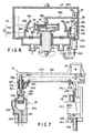
- the lower brush mechanism 40 which serves to wash the back surface of the wafer W, comprises an air cylinder 43, a rod 41, a collective brush 44 and a stage 42 supporting the collective brush 44, as shown in FIG. 8.
- the collective brush 44 is arranged within the wafer holding section 33 of the spin chuck 9 so as to face the back surface of the wafer W held by the spin chuck 9.
- the collective brush 44 consists of a plurality of brushing units and is supported on the stage 42 in a manner to cover substantially a radius of the wafer W.
- the rod 41 extends through the hollow shaft 38 so as to be joined to a lower portion of the stage 42.
- each of the brushing units of the collective brush 44 may be supported rotatable or may be fixed stationary to the stage 42.
- the cup 14, which is arranged to surround the periphery of the spin chuck 9, comprises a cylindrical outer cup member 14b standing from a bottom plate 20 fixed at the bottom portion of the process chamber 12a and a vertically movable inner cup member 12a arranged inside the outer cup member 12b.
- the inner cup member 12a comprises a cylindrical base portion 14c including an upwardly tapered upper region 14d. Also, an inward flange portion 14e is formed at the upper end of the tapered region 14d.
- a vertically movable rod 14g is joined to the inner cup member 14a via a bracket 14f extending from the lower end of the cylindrical base portion 14c.
- the rod 14g is joined to a vertical piston rod 21a of a vertically movable cylinder 21 via a joining member 14h.
- the vertically movable cylinder 21 is arranged outside of the lower end of the process chamber 12a. It follows that the inner cup member 14a is moved up and down by the driving of the vertically movable cylinder 21. When moved to the uppermost position, the inner cup member 14a surrounds the outer circumferential edges of the spin chuck 9 and the wafer W. When the inner cup member 14a is moved to the lowermost position, the upper end of the inner cup member 14a is positioned lower than the spin chuck 9.
- the shutter 13 is joined to the joining member 14h to permit the shutter 13 to be opened or closed by the vertically movable cylinder 21. It follows that the vertical movement of the inner cup member 14a and the opening-closing of the shutter 13 are carried out in synchronism by the driving of the vertically movable cylinder 21.
- a large number of small apertures are formed in the ceiling of the process chamber 12a to permit clean air to be introduced into the process chamber 12a through these small apertures.
- a large number of air passageways 20a are formed concentrically through the bottom plate 20 in the vicinity of the inner wall of the inner cup member 14a. These air passageways 20a communicate with waste liquid and waste gas discharge means (not shown) through a drain passageway 12c formed through the bottom of the process chamber 12a. It follows that a down-flow of air is formed within the process chamber 12a.
- the upper brush mechanism 10 comprises a brush arm 10a as a horizontal moving means, which is joined to a brush arm swinging mechanism 22 and to an upper brush vertical driver 24a via a brush pushing force adjusting mechanism 24.
- a brush 10b is mounted to the free end of the brush arm 10a.
- a motor 25 is mounted on the side of the proximal end of the brush arm 10a.
- a timing belt 25d is stretched between a driving pulley 25b joined to a driving shaft 25a of the motor 25 and a driven pulley 25c joined to a mounting shaft 10c of the brush 10b.
- the rotation of the motor 25 is transmitted by the timing belt 25d to the driven pulley 25c so as to rotate the brush 10b within a horizontal plane about its own vertical axis.
- the rotation of the motor 25 is transmitted by the timing belt 25d to the driven pulley 25c so as to rotate the brush 10b within a horizontal plane about its own vertical axis.
- a brush washing section 26 is formed in the home position of the brush 10b so as to wash the brush 10b itself during non-use of the brush 10b.
- a washing liquid receiving section 10d is formed right above the brush 10b in a manner to surround the shaft 10c.
- a washing liquid (pure water) is supplied through a washing liquid supply pipe 10e into the washing liquid receiving section 10d.
- the pure water is supplied through a plurality of through-holes formed at the bottom portion of the washing liquid receiving section 10d onto the brush 10b and, then, onto the wafer W.
- the mounting shaft 10c extends through a sleeve 10f vertically mounted below the free end of the brush arm 10a.
- a pair of bearings 10g are arranged within the sleeve 10f so as to rotatably support the mounting shaft 10c. The dust generated from the bearings 10g within the sleeve 10f are sucked by a tube 10h.
- the brush pushing force adjusting mechanism 24 comprises a shaft 24b which is rotated by a swing driver 22a and vertically moved by a vertical driver 24a.
- a linear guide 24c is joined to the shaft 24b.
- the linear guide 24c can be swung, swung and vertically moved in accordance with movement of the shaft 24b.
- a connector 24d is mounted below the proximal end of the brush arm 10a and engaged with the linear guide 24c via slider 24e.
- an upper bracket 24j is joined to the connector 24d.
- a compression coil spring 24g is interposed between the upper bracket 24j and the lower bracket 24f.
- the weight of the washing brush mechanism 10 whose vertical movement is guided by the linear guide 24c i.e., the total weight of the brush arm 10a, the brush 10b, etc., is applied to the compression coil spring 24g.
- the pressurizing force applied to the wafer W is controlled by controlling the amount of the downward movement of the slider 24e caused by the vertical driver 24a. In other words, the height of the lowermost point of the brush 10b is adjusted in the case where the brush 10b does not abut against the wafer W and both the slider 24e and the brush arm 10a are downwardly moved together.
- the amount of the downward movement of the slider 24e is assumed to be determined to permit the lower surface of the brush arm 10a to be positioned lower by H mm than the upper surface of the wafer W. If the brush 10b abuts against the wafer W under this condition, the brush 10b is not moved downward to a position lower than the wafer W. Therefore, the spring 24g is elongated by H mm, and an urging force corresponding to the elongation is applied to the brush 10b.
- the brush 10b itself also acts as a spring. It follows that the brush pushing force F can be adjusted within a somewhat allowable range. Since the brush pushing force adjusting mechanism 24 utilizing the spring characteristics of the spring 24b is employed in the present embodiment of the invention, the construction of the apparatus can be simplified, compared with prior art. In addition, the brush pushing force F can be adjusted easily.
- a stopper bearing 24h is mounted below the bracket 24f.
- a shaft supporting the stopper bearing 24h is mounted to the bracket 24f by a screw means such that the bracket 24f is vertically movable within a predetermined range.
- the stopper bearing 24h slides along an arcuate guide plane 24i formed about the center of swinging of the brush arm 10a, with the result that the brush arm 10a is swung under the condition that the brush 10b is in contact with the wafer W. In other words, the brush arm 10a is reversibly swung by the swinging driver 22 in a horizontal plane.
- the arm swinging mechanism 22 comprises a motor 22a.
- a timing belt 22d is stretched between a driving pulley 22b joined to the driving shaft of the motor 22a and a driven pulley 22c.
- a ball screw mechanism is utilized in the vertical driver 24a.
- a brush washing section 26 for washing the brush 10b itself is formed in the waiting position of the upper brush mechanism 10.
- the brush washing section 26 comprises a washing vessel 26a housing the brush 10b.
- a nozzle 26b is arranged to project into an upper open portion of the washing vessel 26a such that a pure water is spurted from an upper position toward the base portion of the brush 10b.
- a waste liquid passageway 26c is formed in the bottom portion of the washing vessel 26a.
- an L-shaped washing liquid supply passageway 26d which is open in the lower end and a side end, is formed in a lower portion of the washing vessel 26a.
- a washing liquid supply pipe (not shown) is connected to the lower end of the washing liquid supply passageway 26d.
- a tube 26e for supplying a washing liquid into the washing vessel 26a is connected to the side end of the washing liquid supply passageway 26d.
- the brush 10b is moved to the waiting position so as to be housed in the washing vessel 26a. Then, the brush 10b is rotated. Under this condition, a washing liquid is spurted from the nozzle 26b toward the base portion of the washing brush mechanism 10 so as to wash away the dust, etc. attached to the brush 10b. The dust, etc. thus removed are discharged to the outside through the waste liquid passageway 26c and, thus, are prevented from being attached again to the brush 10b.
- each of the driving sources of the fifth washing unit 7E is controlled by a control device 80.
- the output section of the control device 80 is connected to the power source of each of the spin chuck driving motor 19, a rotation changeover switch 18, the upper brush arm swinging motor 22a, the upper brush swinging motor 25, an upper brush vertical driver 24a, a lower brush vertical driver 43, and an inner cup member vertical driving cylinder 21.
- the rotation changeover switch 18 serves to changeover the rotation of the spin chuck driving motor 19 in the clockwise direction and the counter clockwise direction.
- the control device 80 controls the rotation changeover switch 18 to permit the rotating direction of the spin chuck 9 to be changed every predetermined period of time.
- the tendency of contaminants present on the washing surface of the wafer W before the washing treatment is stored in a memory of the control device 80 as initial data.
- the data for controlling the moving speed (swinging speed) of the brush arm 10a is stored as the initial data.
- the tendency of contaminants noted above corresponds to the actual data obtained through experiences from the actual manufacturing process.
- the initial data is read out of the memory in the control device 80 so as to control the operation of each of the driving sources 18, 19, 22a, 25, 24a, 43 and 21.
- the state of contaminants present on the washing surface of the wafer W is detected by using the optical sensors 28, 29 shown in FIGS. 11A and 11B, and the detected data is supplied to the control device 80 so as to control the operation of each of the driving sources 18, 19, 22a, 25, 24a, 43 and 21.
- FIG. 12 is a flow chart showing the operation of the wafer washing apparatus described above.
- the cassette CR housing a predetermined number of wafers W is set on the cassette table 4 in the cassette section 2. If the wafer washing apparatus 1 is started up by depressing a start-up button under this condition, the shutter 13 is opened by the cylinder 21 (step S1). In this step, the inner cup member 14b is moved downward together with the shutter 13. On the other hand, the wafer W is taken out of the cassette CR by the sub-arm mechanism 5 so as to be delivered to the main arm mechanism 6. Then, the wafer W is loaded in the process chamber 12a through the opening 12b (step S2). Further, the wafer W is transferred from the holder of the main arm mechanism 6 onto the spin chuck 9, followed by retreating the holder of the main arm mechanism 6 from within the process chamber 12a and subsequently closing the shutter 13 (step S3).
- the upper and lower brushes 10b and 44 are moved so as to be aligned with the wafer W held on the spin chuck 9 (step S4). Under this condition, the wafer W is rotated together with the spin chuck 9 (step S5) and the upper and lower brushes 10b, 44 are brought into contact with the wafer W while supplying a washing liquid (pure water) onto both surfaces of the wafer W.
- the stroke of the downward movement of the upper brush 10b is controlled by the vertical driver mechanism 24 so as to control the pushing force of the upper brush 10b against the wafer W. Also, the upper brush 10b is rotated.
- step S5 the motor 22a is started so as to swing the arm 10a and move the upper brush 10b relative to the rotating wafer W (step S5).
- the upper brush 10b is moved in a radial direction of the wafer W from a central portion toward a peripheral portion of the wafer W.
- the scrubbing operation of the upper brush 10b is controlled in accordance with the stained state of the washing region of the wafer W (step S7).
- step S7 the initial data is read out of the memory of the control device 80 so as to control the scrubbing operation based on the data read out of the control device 80.
- the data used in this step may be either the initial data (data inputted by input means 82) on the relationship between the surface state of the wafer W and the scrubbing operation, said data being stored in advance in the memory of the control device 80, or the data on the surface state of the wafer W, which was detected in advance by the inspection unit 8.
- the scrubbing operation of the brush is controlled in accordance with the stained state of the washing region of the wafer W so as to remove efficiently the contaminants from the surface of the wafer W.
- the upper brush 10b it is possible for the upper brush 10b to be freely rotatable. Also, the upper brush 10b may be allowed to contact the washing liquid alone without bringing the upper brush 10b into direct contact with the upper surface of the substrate.
- step S8 After the scrubbing operation, the movement of the upper brush 10b relative to the wafer W is stopped (step S8). Then, the upper brush 10b is moved into the waiting section 26, and the lower brush 44 is retreated downward (step S9). After the brush-washing treatment, the jet water spurting nozzle 15 is moved to a region above the wafer W, as required, so as to spurt a jet water onto the wafer W for washing the wafer W with the jet water.
- step S10 pure water is applied to both surfaces of the wafer W for the rinsing purpose.
- step S11 the spin chuck 9 is rotated at a high speed for centrifugally removing the applied water from the wafer W (step S11), followed by opening the shutter 13 (step S12 and subsequently unloading the washed wafer W from within the process chamber 20a by the main arm mechanism 6 (step S13).
- step S14 the shutter 13 is closed
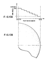
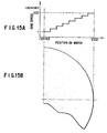
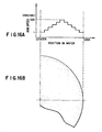
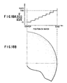
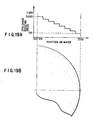
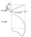
- FIGS. 13A to 20B show various modes of the scrubbing operation control step S7.
- the control device 80 controls the operation of the brush arm swinging mechanism 22 to permit the brush arm 10a to be moved at a high speed in a central portion of the wafer W and at a low speed in a peripheral portion of the wafer W as shown in FIG. 13A.
- the moving speed of the brush arm 10a is changed stepwise ranging between 300 mm/sec in a central portion of the wafer W and 1 mm/sec in the outermost peripheral portion of the wafer W.
- the peripheral portion of the wafer W is scrubbed with the brush 10b for a longer time, with the result that the peripheral portion is washed sufficiently so as to remove effectively the contaminants attached to the peripheral portion.
- the scrubbing time of the wafer W with the brush 10b is short, making it possible to prevent the difficulty that the contaminants attached to the brush 10b are transferred onto the wafer surface so as to stain the wafer surface.
- the control device 80 controls the operation of the brush arm swinging mechanism 22 to permit the brush arm 10a to be moved at a high speed in a central portion of the wafer W and at a low speed in a peripheral portion of the wafer W as shown in FIG. 14A.
- the moving speed of the brush arm 10a is changed continuously from 300 mm/sec in a central portion of the wafer W to 1 mm/sec in the outermost peripheral portion of the wafer W.
- the control device 80 controls the operation of the brush arm swinging mechanism 22 to permit the brush arm 10a to be moved at a low speed in a central portion of the wafer W and at a high speed in a peripheral portion of the wafer W as shown in FIG. 15A.
- the moving speed of the brush arm 10a is changed stepwise ranging between 1 mm/sec in a central portion of the wafer W and 300 mm/sec in the outermost peripheral portion of the wafer W.
- the control device 80 controls the operation of the brush arm swinging mechanism 22 to permit the brush arm 10a to be moved at a low speed in a central portion and the outermost peripheral portion of the wafer W and at a high speed in a region intermediate between the central portion and the outermost peripheral portion of the wafer W as shown in FIG. 16A.
- the moving speed of the brush arm 10a is changed stepwise ranging between 1 mm/sec in the central portion and the outermost peripheral portion of the wafer W and 300 mm/sec in the region intermediate between the central portion and the outermost peripheral portion of the wafer W.
- the control device 80 controls the operation of the brush vertical driver 24a to permit the contact pressure of the upper brush 10b to be lower in a central portion of the wafer W and higher in a peripheral portion of the wafer W as shown in FIG. 17A.
- the contact pressure of the upper brush 10b against the wafer W is changed stepwise ranging between 10 g in a central portion of the wafer W and 200 g in the outermost peripheral portion of the wafer W.
- the control device 80 controls the operation of the brush rotating motor 25 to permit the rotating speed of the upper brush 10b to be lower in a central portion of the wafer W and higher in a peripheral portion of the wafer W as shown in FIG. 18A.
- the rotating speed of the upper brush 10b is changed stepwise ranging between 10 rpm in a central portion of the wafer W and 300 rpm in the outermost peripheral portion of the wafer W.
- the control device 80 controls the operation of the spin chuck driving motor 19 to permit the rotating speed of the spin chuck 9 to be higher when the upper brush 10b is in contact with the central portion of the wafer W and to be lower when the upper brush 10b is in contact with the peripheral portion of the wafer W.
- the rotating speed of the spin chuck 9 is changed stepwise ranging between 5000 rpm when the upper brush 10b is in contact with the central portion of the wafer W and 100 rpm when the upper brush 10b is in contact with the peripheral portion of the wafer W.
- the control device 80 controls the operation of the spin chuck driving motor 19 to permit the rotating speed of the spin chuck 9 to be lower when the upper brush 10b is in contact with the central portion of the wafer W and to be higher when the upper brush 10b is in contact with the peripheral portion of the wafer W.
- the rotating speed of the spin chuck 9 is changed stepwise ranging between 5000 rpm when the upper brush 10b is in contact with the outermost peripheral portion of the wafer W and 100 rpm when the upper brush 10b is in contact with the central portion of the wafer W.
- the brush 10b is kept in contact with the outermost peripheral portion of the wafer W for a long time, making it possible to remove effectively the contaminants from the outermost peripheral portion of the wafer W.
- the method shown in FIG. 20 is exceptional.
- the contact time between the outermost peripheral portion of the wafer W and the brush 10b is short, with the result that the particles generated from the brush 10b are effectively prevented from being attached again to the outermost peripheral portion of the wafer W.
- the nozzle arm 10a and the jet water spurting nozzle 15 are formed as separate members. However, it is also possible to allow the nozzle arm 10a to perform the function of spurting a jet water. In this case, the space for mounting the jet water spurting nozzle 15 can be omitted. Also, the time for the washing treatment can be shortened because a jet water can be spurted immediately after sliding of the brush 10b.
- a semiconductor wafer is used as an object to be washed.
- the technical idea of the present invention can also be applied to the washing of, for example, a glass substrate for LCD.
Landscapes
- Cleaning Or Drying Semiconductors (AREA)
- Cleaning In General (AREA)
- Cleaning By Liquid Or Steam (AREA)
Claims (20)
- Appareil pour nettoyer un substrat comprenant :un mandrin tournant (9) pour porter et faire tourner un substrat à nettoyer ;des moyens de nettoyage (10) pour fournir un liquide de nettoyage sur une surface du substrat porté par le mandrin tournant et appliquer une force physique à des contaminants présents sur une surface du substrat de façon à ôter lesdits contaminants ;un bras de support (10) pour supporter les moyens de nettoyage ; et,un mécanisme d'entraínement pour le bras (22), pour entraíner le bras de support de façon à déplacer les moyens de nettoyage à la surface, depuis une zone centrale vers une zone périphérique du substrat ;caractérisé par des moyens (28, 29, 82) adaptés pour fournir des données relative à la distribution des contaminants sur la surface du substrat ; et,des moyens de commande (80) en communication avec lesdits moyens adaptés pour fournir des données relatives à la distribution, lesdits moyens de commande étant adaptés pour commander le fonctionnement d'au moins l'un parmi les moyens de nettoyage, le mandrin tournant et le mécanisme d'entraínement de l'arbre, de façon à commander la force physique agissant sur les contaminants présents sur la surface du substrat en accord avec les données de distribution reçues des moyens adaptés pour fournir des données relatives à la distribution.
- Appareil selon la revendication 1, caractérisé en ce que lesdits moyens adaptés à fournir des données relatives à la distribution, comprennent un capteur (28, 29) pour détecter la distribution des contaminants présents à la surface du substrat avant le traitement de nettoyage.
- Appareil selon la revendication 1, caractérisé en ce que les moyens adaptés à fournir des données relatives à la distribution, comprennent des moyens adaptés pour stocker des données de distribution, relatives à des processus de fabrication précédents, de contaminants à la surfaces de substrats, avant le nettoyage.
- Appareil selon la revendication 1, caractérisé en ce que les moyens de nettoyage (10) comprennent une brosse (10b) entraínée en rotation pour brosser la surface du substrat et des moyens de commutation (18) pour changer la direction de rotation de la brosse (10b) entre une direction horaire et une direction antihoraire.
- Appareil selon la revendication 4, caractérisé en ce qu'il comprend en outre un mécanisme presseur (24) pour une brosse, pour appuyer ladite brosse entraínée en rotation sur la surface du substrat ;
dans lequel lesdits moyens de commande (80) sont adaptés pour commander le mécanisme de pression (24) pour une brosse de façon à ce que la pression de contact de la brosse entraínée en rotation (10b) appliquée à la surface du substrat soit progressivement augmentée ou progressivement diminuée lorsque lesdits moyens de nettoyage (10) sont déplacés par ledit mécanisme d'entraínement du bras (22) depuis une zone centrale vers une zone périphérique du substrat. - Appareil selon la revendication 4, caractérisé en ce qu'il comprend en outre un mécanisme variable de rotation de brosse, pour augmenter ou diminuer progressivement la vitesse de rotation de la brosse entraínée en rotation ;
dans lequel lesdits moyens de commande (80) sont adaptés à commander ledit mécanisme variable de rotation de brosse (25) de façon à ce que la vitesse de rotation de la brosse entraínée en rotation (10b) soit progressivement augmentée ou progressivement diminuée lorsque lesdits moyens de nettoyage (10) sont déplacés par ledit mécanisme d'entraínement du bras (22) depuis une zone centrale vers une zone périphérique du substrat. - Appareil selon la revendication 1, caractérisé en ce que les moyens de nettoyage (10) comprennent une brosse qui est mobile en rotation autour d'un arbre de support vertical (10c) et qui est conçue pour entrer en contact avec un substrat maintenu horizontal par le mandrin tournant (9).
- Appareil selon la revendication 1, caractérisé en ce que ledit mécanisme d'entraínement d'un bras (22), comprend un mécanisme de balancement de bras (22a à 22d) pour faire se balancer ledit bras de support pour permettre aux moyens de nettoyage de se déplacer le long de la surface du substrat selon une direction radiale relativement au substrat, et en ce que lesdits moyens de commande (80) sont adaptés pour faire en sorte que le mécanisme de balancement de bras (22a à 22d) fasse progressivement augmenter ou diminuer la vitesse de déplacement des moyens de nettoyage (10) tandis que le mécanisme d'entraínement de bras (22) déplace les moyens de nettoyage (10) depuis une zone centrale vers une zone périphérique du substrat.
- Appareil selon la revendication 1, caractérisé en ce qu'il comprend en outre un mécanisme de variation de rotation pour un mandrin tournant pour augmenter ou diminuer la vitesse de rotation du mandrin tournant ;
dans lequel lesdits moyens de contrôle (80) sont adaptés pour faire en sorte que le mécanisme (19) de variation de rotation de mandrin tournant fasse progressivement augmenter ou diminuer la vitesse de rotation du mandrin tournant (9) lorsque le mécanisme d'entraínement de bras (22) déplace les moyens de nettoyage (10) depuis une zone centrale vers une zone périphérique du substrat. - Appareil selon la revendication 1, caractérisé en ce que lesdits moyens de nettoyage (10) comprennent un mécanisme de nettoyage par onde ultrasonique (7A, 7B) pour appliquer une onde ultrasonique à la surface du substrat couvert avec le liquide de nettoyage.
- Appareil selon la revendication 1, caractérisé en ce que lesdits moyens de nettoyage (10) comprennent un mécanisme de nettoyage par jet d'eau sous pression (7C) pour projeter de l'eau sous haute pression contre la surface du substrat.
- Appareil selon la revendication 1, caractérisé en ce que lesdits moyens de nettoyage (10) comprennent un premier mécanisme de brosse (10b à 10h) pour nettoyer par brossage une surface d'un substrat, ladite surface formant un motif, et un deuxième mécanisme de brosse (41, 43, 44) pour nettoyer par brossage la surface du substrat sur laquelle un motif n'est pas formé.
- Appareil selon la revendication 1, caractérisé en ce qu'il comprend en outre une buse (15) pour fournir un liquide de rinçage sur la surface du substrat.
- Procédé pour nettoyer un substrat, caractérisé en ce qu'il comprend les étapes suivantes :a) maintenir le substrat avec un mandrin tournant ;b) aligner des moyens de nettoyage, montés sur un bras supporté de façon mobile par un mécanisme d'entraínement de bras, relativement à la surface du substrat porté par le mandrin tournant ;c) Faire tourner le substrat en même temps que le mandrin tournant ; et,d) fournir un liquide de nettoyage sur la surface à nettoyer du substrat qui est maintenu en rotation ;
caractérisé en ce que :e) on détermine la distribution de contaminants présents à la surface du substrat à nettoyer ; et,f) on commande le fonctionnement d'au moins l'un parmi les moyens de nettoyage, le mandrin tournant et le mécanisme d'entraínement de bras, de façon à commander la force qui est appliquée sur les contaminants présents sur la surface du substrat, en accord avec la distribution des contaminants déterminée à l'étape (e), de façon à enlever les contaminants. - Procédé selon la revendication 14, caractérisé en ce que l'étape (e) consiste à détecter la distribution de contaminants présents sur la surface du substrat avant le traitement de nettoyage en utilisant un capteur (28, 29), et en ce qu'au moins l'un parmi les moyens de nettoyage, le mandrin tournant et le mécanisme d'entraínement de bras est commandé lors de ladite étape (f) sur la base du résultat de la détection.
- Procédé selon la revendication 14, caractérisé en ce que l'étape (e) consiste à obtenir la distribution des contaminants présents sur la surface de substrats avant le traitement de nettoyage dans des processus de fabrication précédents et au stockage de ladite distribution dans les moyens de commande en tant que données d"initialisation, et en ce que les données d'initialisation sont lues lors de ladite étape (f) de façon à commander au moins l'un parmi les moyens de nettoyage, le mandrin tournant et le mécanisme d'entraínement de bras sur la base des données d'initialisation.
- Procédé selon la revendication 14, caractérisé en ce que les moyens de nettoyage comprennent une brosse entraínée en rotation pour brosser la surface du substrat, et en ce que la vitesse de rotation de ladite brosse entraínée en rotation est progressivement augmentée ou progressivement diminuée lors de ladite étape (f) pendant que le mécanisme d'entraínement du bras déplace les moyens de nettoyage depuis une zone centrale vers une zone périphérique du substrat.
- Procédé selon la revendication 17, caractérisé en ce que la pression de contact, de la brosse entraínée en rotation, appliquée sur le substrat est progressivement augmentée ou progressivement diminuée lors de ladite étape (f) pendant que le mécanisme d'entraínement de bras déplace les moyens de nettoyage depuis une zone centrale vers une zone périphérique du substrat.
- Procédé selon la revendication 14, caractérisé en ce que la vitesse de rotation du mandrin tournant est progressivement augmentée ou progressivement diminuée lors de ladite étape (f) pendant que le mécanisme d'entraínement du bras déplace les moyens de nettoyage depuis une zone centrale vers une zone périphérique du substrat.
- Procédé selon la revendication 14, caractérisé en ce que deux surfaces du substrat sont simultanément nettoyées lors de l'étape (f).
Applications Claiming Priority (3)
| Application Number | Priority Date | Filing Date | Title |
|---|---|---|---|
| JP197226/97 | 1997-07-23 | ||
| JP19722697 | 1997-07-23 | ||
| JP19722697A JP3320640B2 (ja) | 1997-07-23 | 1997-07-23 | 洗浄装置 |
Publications (3)
| Publication Number | Publication Date |
|---|---|
| EP0893819A2 EP0893819A2 (fr) | 1999-01-27 |
| EP0893819A3 EP0893819A3 (fr) | 2000-08-02 |
| EP0893819B1 true EP0893819B1 (fr) | 2005-10-26 |
Family
ID=16370946
Family Applications (1)
| Application Number | Title | Priority Date | Filing Date |
|---|---|---|---|
| EP98113546A Expired - Lifetime EP0893819B1 (fr) | 1997-07-23 | 1998-07-21 | Dispositif et méthode pour le lavage de substrat |
Country Status (5)
| Country | Link |
|---|---|
| US (1) | US6059891A (fr) |
| EP (1) | EP0893819B1 (fr) |
| JP (1) | JP3320640B2 (fr) |
| KR (1) | KR100568388B1 (fr) |
| DE (1) | DE69832011T2 (fr) |
Families Citing this family (41)
| Publication number | Priority date | Publication date | Assignee | Title |
|---|---|---|---|---|
| US6261378B1 (en) * | 1998-03-23 | 2001-07-17 | Tokyo Electron Limited | Substrate cleaning unit and cleaning method |
| US6290780B1 (en) * | 1999-03-19 | 2001-09-18 | Lam Research Corporation | Method and apparatus for processing a wafer |
| US20010014498A1 (en) * | 1999-04-30 | 2001-08-16 | Gregory M. Amico | Method and apparatus for forming an inlaid capacitor in a semiconductor wafer |
| US6711775B2 (en) * | 1999-06-10 | 2004-03-30 | Lam Research Corporation | System for cleaning a semiconductor wafer |
| JP3990073B2 (ja) * | 1999-06-17 | 2007-10-10 | 株式会社荏原製作所 | 基板洗浄装置及び基板洗浄方法 |
| KR20010037210A (ko) * | 1999-10-14 | 2001-05-07 | 구본준, 론 위라하디락사 | 기판 세정 장치 및 기판 세정 방법 |
| US6415804B1 (en) * | 1999-12-23 | 2002-07-09 | Lam Research Corporation | Bowl for processing semiconductor wafers |
| JP2001246331A (ja) * | 2000-03-08 | 2001-09-11 | Sharp Corp | 洗浄装置 |
| FR2808120B1 (fr) * | 2000-04-20 | 2002-07-26 | Karl Suss France | Procede et dispositif pour le traitement du substrat d'un circuit integre ou d'un produit analogue en cours de fabrication |
| US6418584B1 (en) | 2000-05-24 | 2002-07-16 | Speedfam-Ipec Corporation | Apparatus and process for cleaning a work piece |
| KR100877044B1 (ko) * | 2000-10-02 | 2008-12-31 | 도쿄엘렉트론가부시키가이샤 | 세정처리장치 |
| US6530103B2 (en) * | 2001-06-21 | 2003-03-11 | Taiwan Semiconductor Manufacturing Company, Ltd. | Method and apparatus for eliminating wafer breakage during wafer transfer by a vacuum pad |
| US7171973B2 (en) * | 2001-07-16 | 2007-02-06 | Tokyo Electron Limited | Substrate processing apparatus |
| US20030029479A1 (en) * | 2001-08-08 | 2003-02-13 | Dainippon Screen Mfg. Co, Ltd. | Substrate cleaning apparatus and method |
| JP2003068695A (ja) * | 2001-08-29 | 2003-03-07 | Hitachi Ltd | 半導体集積回路装置の製造方法 |
| KR100445259B1 (ko) * | 2001-11-27 | 2004-08-21 | 삼성전자주식회사 | 세정방법 및 이를 수행하기 위한 세정 장치 |
| US6807972B2 (en) * | 2002-03-29 | 2004-10-26 | Applied Materials, Inc. | Gutter and splash-guard for protecting a wafer during transfer from a single wafer cleaning chamber |
| JP4105931B2 (ja) * | 2002-10-31 | 2008-06-25 | ラムリサーチ株式会社 | 対象物処理装置およびその方法 |
| KR100648165B1 (ko) | 2004-04-06 | 2006-11-28 | 동경 엘렉트론 주식회사 | 기판 세정 장치, 기판 세정 방법 및 그 방법에 사용되는프로그램을 기록한 매체 |
| KR100757093B1 (ko) * | 2005-07-20 | 2007-09-10 | 주식회사 룩스비타 | 카메라 모듈의 재생방법 |
| JP2007220890A (ja) | 2006-02-16 | 2007-08-30 | Toshiba Corp | 塗布現像処理装置における基板周縁処理方法 |
| JP2007273608A (ja) * | 2006-03-30 | 2007-10-18 | Dainippon Screen Mfg Co Ltd | 基板処理装置および基板処理方法 |
| KR100892809B1 (ko) | 2006-03-30 | 2009-04-10 | 다이닛뽕스크린 세이조오 가부시키가이샤 | 기판처리장치 및 기판처리방법 |
| JP4813430B2 (ja) * | 2007-07-12 | 2011-11-09 | 東京エレクトロン株式会社 | 基板洗浄装置、基板洗浄方法、および記録媒体 |
| TWI372661B (en) * | 2007-11-21 | 2012-09-21 | Tokyo Electron Ltd | Cleaning apparatus and cleaning method |
| KR101004435B1 (ko) | 2008-11-28 | 2010-12-28 | 세메스 주식회사 | 기판 연마 장치 및 이를 이용한 기판 연마 방법 |
| JP4751927B2 (ja) * | 2008-12-01 | 2011-08-17 | 芝浦メカトロニクス株式会社 | スピン処理装置 |
| US8468637B2 (en) * | 2009-02-06 | 2013-06-25 | Endoclear Llc | Mechanically-actuated endotracheal tube cleaning device |
| JP5535687B2 (ja) * | 2010-03-01 | 2014-07-02 | 株式会社荏原製作所 | 基板洗浄方法及び基板洗浄装置 |
| JP5661564B2 (ja) * | 2011-06-10 | 2015-01-28 | 株式会社荏原製作所 | 洗浄性能予測方法及び基板洗浄方法 |
| US20130092186A1 (en) | 2011-10-18 | 2013-04-18 | Taiwan Semiconductor Manufacturing Company, Ltd. | Removal of particles on back side of wafer |
| US20140310895A1 (en) * | 2013-04-19 | 2014-10-23 | Applied Materials, Inc. | Scrubber brush force control assemblies, apparatus and methods for chemical mechanical polishing |
| JP6054805B2 (ja) * | 2013-04-25 | 2016-12-27 | 株式会社荏原製作所 | 基板洗浄装置 |
| US9839942B1 (en) | 2014-01-16 | 2017-12-12 | Texas Nameplate Company, Inc. | System for and method of by-product removal from a metal substrate |
| KR102004109B1 (ko) | 2014-10-31 | 2019-07-25 | 가부시키가이샤 에바라 세이사꾸쇼 | 기판 세정 장치 및 기판 세정 방법 |
| JP6740065B2 (ja) * | 2016-09-13 | 2020-08-12 | 株式会社Screenホールディングス | 基板洗浄装置、基板処理装置、基板洗浄方法および基板処理方法 |
| JP7149869B2 (ja) * | 2019-02-07 | 2022-10-07 | 株式会社荏原製作所 | 基板洗浄方法および基板洗浄装置 |
| KR20200101638A (ko) | 2019-02-20 | 2020-08-28 | 장정원 | 세척기능을 포함한 오븐기 |
| US11256180B2 (en) * | 2019-04-29 | 2022-02-22 | Taiwan Semiconductor Manufacturing Co., Ltd. | Processing apparatus and method thereof |
| CN113042425B (zh) * | 2021-04-30 | 2022-04-29 | 深圳源明杰科技股份有限公司 | 一种智能卡表面清洗机 |
| CN115870295B (zh) * | 2022-12-05 | 2023-10-03 | 苏州天准科技股份有限公司 | 用于载具中玻璃镜片的下表面全自动清洁装置和清洁方法 |
Family Cites Families (58)
| Publication number | Priority date | Publication date | Assignee | Title |
|---|---|---|---|---|
| JPS5861632A (ja) * | 1981-10-07 | 1983-04-12 | Matsushita Electric Ind Co Ltd | 洗浄槽 |
| JPS5866333A (ja) * | 1981-10-14 | 1983-04-20 | Matsushita Electric Ind Co Ltd | 洗浄槽 |
| JPS6148258A (ja) * | 1984-08-15 | 1986-03-08 | Toshiba Corp | シリアルデ−タ伝送装置 |
| JPS6116528A (ja) * | 1985-06-14 | 1986-01-24 | Hitachi Ltd | ウエハ洗浄装置 |
| US4795497A (en) * | 1985-08-13 | 1989-01-03 | Mcconnell Christopher F | Method and system for fluid treatment of semiconductor wafers |
| JPS6247153A (ja) * | 1985-08-27 | 1987-02-28 | Ibiden Co Ltd | 半導体装置 |
| JPS62252147A (ja) * | 1986-04-25 | 1987-11-02 | Hitachi Ltd | 半導体ウエハ移し替え装置 |
| JPS6438721A (en) * | 1987-08-04 | 1989-02-09 | Fujikura Ltd | Branching ratio variable type optical fiber coupler |
| JPH01120828A (ja) * | 1987-11-04 | 1989-05-12 | Oki Electric Ind Co Ltd | 半導体ウエハの自動洗浄装置 |
| JPH01184926A (ja) * | 1988-01-20 | 1989-07-24 | Matsushita Electric Ind Co Ltd | 洗浄装置および洗浄方法 |
| KR970003907B1 (ko) * | 1988-02-12 | 1997-03-22 | 도오교오 에레구토론 가부시끼 가이샤 | 기판처리 장치 및 기판처리 방법 |
| JPH02130827A (ja) * | 1988-11-10 | 1990-05-18 | Mitsubishi Electric Corp | 半導体基板の洗浄方法およびそれに用いる洗浄装置 |
| US5061144A (en) * | 1988-11-30 | 1991-10-29 | Tokyo Electron Limited | Resist process apparatus |
| KR0134962B1 (ko) * | 1989-07-13 | 1998-04-22 | 나까다 구스오 | 디스크 세척장치 |
| JP2746669B2 (ja) * | 1989-07-20 | 1998-05-06 | 東京エレクトロン株式会社 | 洗浄装置及び洗浄方法 |
| JP2746670B2 (ja) * | 1989-07-20 | 1998-05-06 | 東京エレクトロン株式会社 | 洗浄装置 |
| JP2683940B2 (ja) * | 1989-08-09 | 1997-12-03 | 信越半導体 株式会社 | ワークの自動洗浄装置 |
| JPH03116731A (ja) * | 1989-09-28 | 1991-05-17 | Dan Kagaku:Kk | 半導体ウエハ用移送装置 |
| JPH0414494A (ja) * | 1990-05-07 | 1992-01-20 | Toppan Printing Co Ltd | 印刷物 |
| JPH0415920A (ja) * | 1990-05-09 | 1992-01-21 | Mitsubishi Electric Corp | ウエハの洗浄用保持装置およびその洗浄方法 |
| JPH0456321A (ja) * | 1990-06-26 | 1992-02-24 | Fujitsu Ltd | 半導体ウエハの洗浄装置 |
| JP2926944B2 (ja) * | 1990-09-18 | 1999-07-28 | 松下電器産業株式会社 | 光ディスク装置用クリーナー |
| JPH04130724A (ja) * | 1990-09-21 | 1992-05-01 | Hitachi Ltd | 洗浄装置 |
| JP3165435B2 (ja) * | 1990-11-17 | 2001-05-14 | 東京エレクトロン株式会社 | 洗浄装置 |
| US5226437A (en) * | 1990-11-28 | 1993-07-13 | Tokyo Electron Limited | Washing apparatus |
| JP3214503B2 (ja) * | 1990-11-28 | 2001-10-02 | 東京エレクトロン株式会社 | 洗浄装置 |
| JP3162704B2 (ja) * | 1990-11-28 | 2001-05-08 | 東京エレクトロン株式会社 | 処理装置 |
| US5297910A (en) * | 1991-02-15 | 1994-03-29 | Tokyo Electron Limited | Transportation-transfer device for an object of treatment |
| US5144711A (en) * | 1991-03-25 | 1992-09-08 | Westech Systems, Inc. | Cleaning brush for semiconductor wafer |
| JPH04304652A (ja) * | 1991-04-01 | 1992-10-28 | Hitachi Ltd | 熱処理装置用ボート |
| JP2901098B2 (ja) * | 1991-04-02 | 1999-06-02 | 東京エレクトロン株式会社 | 洗浄装置および洗浄方法 |
| JP2913119B2 (ja) * | 1991-05-07 | 1999-06-28 | 東京エレクトロン株式会社 | 被洗浄体の移載方法及びその装置並びに被移載体の位置決め装置 |
| JPH0553241A (ja) * | 1991-06-10 | 1993-03-05 | Fuji Photo Film Co Ltd | ハロゲン化銀写真感光材料 |
| JPH0536815A (ja) * | 1991-07-25 | 1993-02-12 | Canon Inc | ウエハ搬送装置 |
| JPH0536814A (ja) * | 1991-07-31 | 1993-02-12 | Sony Corp | ウエハ移載装置 |
| JPH05121361A (ja) * | 1991-10-28 | 1993-05-18 | Mitsubishi Electric Corp | 半導体ウエハ冷却装置 |
| JPH05182946A (ja) * | 1991-12-27 | 1993-07-23 | Shimada Phys & Chem Ind Co Ltd | 洗浄装置 |
| JP2571487B2 (ja) * | 1991-12-27 | 1997-01-16 | 信越半導体株式会社 | 薄円板状ワークのスクラバー洗浄装置 |
| US5327921A (en) * | 1992-03-05 | 1994-07-12 | Tokyo Electron Limited | Processing vessel for a wafer washing system |
| JP3113411B2 (ja) * | 1992-03-18 | 2000-11-27 | 東京エレクトロン株式会社 | 洗浄装置 |
| US5345639A (en) * | 1992-05-28 | 1994-09-13 | Tokyo Electron Limited | Device and method for scrubbing and cleaning substrate |
| JP2739419B2 (ja) * | 1992-09-25 | 1998-04-15 | 大日本スクリーン製造株式会社 | 基板処理装置 |
| JP3194209B2 (ja) * | 1992-11-10 | 2001-07-30 | 東京エレクトロン株式会社 | 洗浄処理装置 |
| JP3052105B2 (ja) * | 1992-11-20 | 2000-06-12 | 東京エレクトロン株式会社 | 洗浄処理装置 |
| US5503171A (en) * | 1992-12-26 | 1996-04-02 | Tokyo Electron Limited | Substrates-washing apparatus |
| JP3347814B2 (ja) * | 1993-05-17 | 2002-11-20 | 大日本スクリーン製造株式会社 | 基板の洗浄・乾燥処理方法並びにその処理装置 |
| US5509464A (en) * | 1993-07-30 | 1996-04-23 | Applied Materials, Inc. | Method and apparatus for cooling rectangular substrates |
| US5518542A (en) * | 1993-11-05 | 1996-05-21 | Tokyo Electron Limited | Double-sided substrate cleaning apparatus |
| US5626675A (en) * | 1993-11-18 | 1997-05-06 | Tokyo Electron Limited | Resist processing apparatus, substrate processing apparatus and method of transferring a processed article |
| JP3328426B2 (ja) * | 1994-05-12 | 2002-09-24 | 東京エレクトロン株式会社 | 洗浄装置 |
| KR0171491B1 (ko) * | 1994-09-20 | 1999-03-30 | 이시다 아키라 | 회전식 기판세정장치 |
| JP3539787B2 (ja) * | 1995-03-09 | 2004-07-07 | 大日本スクリーン製造株式会社 | 回転式基板洗浄装置 |
| JPH08148459A (ja) * | 1994-11-18 | 1996-06-07 | Toshiba Corp | 半導体基板の洗浄方法 |
| US5730162A (en) * | 1995-01-12 | 1998-03-24 | Tokyo Electron Limited | Apparatus and method for washing substrates |
| TW316995B (fr) * | 1995-01-19 | 1997-10-01 | Tokyo Electron Co Ltd | |
| JPH0949802A (ja) * | 1995-08-09 | 1997-02-18 | Shin Etsu Handotai Co Ltd | パーティクルの検査方法 |
| JPH09148295A (ja) * | 1995-11-27 | 1997-06-06 | Dainippon Screen Mfg Co Ltd | 回転式基板処理装置 |
| US5865901A (en) * | 1997-12-29 | 1999-02-02 | Siemens Aktiengesellschaft | Wafer surface cleaning apparatus and method |
-
1997
- 1997-07-23 JP JP19722697A patent/JP3320640B2/ja not_active Expired - Fee Related
-
1998
- 1998-07-21 DE DE69832011T patent/DE69832011T2/de not_active Expired - Lifetime
- 1998-07-21 EP EP98113546A patent/EP0893819B1/fr not_active Expired - Lifetime
- 1998-07-22 US US09/120,551 patent/US6059891A/en not_active Expired - Lifetime
- 1998-07-23 KR KR1019980029745A patent/KR100568388B1/ko not_active Expired - Lifetime
Also Published As
| Publication number | Publication date |
|---|---|
| KR100568388B1 (ko) | 2006-07-11 |
| KR19990014121A (ko) | 1999-02-25 |
| EP0893819A3 (fr) | 2000-08-02 |
| EP0893819A2 (fr) | 1999-01-27 |
| DE69832011T2 (de) | 2006-07-27 |
| JP3320640B2 (ja) | 2002-09-03 |
| US6059891A (en) | 2000-05-09 |
| JPH1140530A (ja) | 1999-02-12 |
| DE69832011D1 (de) | 2005-12-01 |
Similar Documents
| Publication | Publication Date | Title |
|---|---|---|
| US6059891A (en) | Apparatus and method for washing substrate | |
| KR101118655B1 (ko) | 폴리싱장치 및 기판처리장치 | |
| US7850817B2 (en) | Polishing device and substrate processing device | |
| US7416474B2 (en) | Planarization apparatus | |
| KR101042762B1 (ko) | 기판처리장치 및 기판처리방법 | |
| JP3321725B2 (ja) | 洗浄装置 | |
| KR20140034273A (ko) | 기판 세정 방법 및 기판 세정 장치 | |
| US6491760B2 (en) | Scrub washing method | |
| JP2001038614A (ja) | 研磨装置 | |
| JP2001070896A (ja) | 基板洗浄装置 | |
| KR101977771B1 (ko) | 기판 처리 장치 | |
| JP3616725B2 (ja) | 基板の処理方法及び処理装置 | |
| US10376929B2 (en) | Apparatus and method for polishing a surface of a substrate | |
| KR102270937B1 (ko) | 기판 처리 장치 및 방법 | |
| JP2909432B2 (ja) | スピン洗浄処理ユニット | |
| JP7510473B2 (ja) | 基板処理装置及び基板処理方法 | |
| KR20030067391A (ko) | 화학기계적 연마장치 | |
| US7155963B2 (en) | Cleaning evaluation method for a substrate | |
| JP2000208466A (ja) | 基板処理方法および基板処理装置 | |
| JP4150116B2 (ja) | 基板の処理装置 | |
| KR102798418B1 (ko) | 기판 세정 장치 | |
| JPH11204472A (ja) | 基板研磨装置用光学測定装置 | |
| JPH11219881A (ja) | 基板処理装置 | |
| KR20190008458A (ko) | 기판 처리 장치 및 방법 | |
| KR20260047461A (ko) | 기판 처리 장치 및 기판 처리 방법 |
Legal Events
| Date | Code | Title | Description |
|---|---|---|---|
| PUAI | Public reference made under article 153(3) epc to a published international application that has entered the european phase |
Free format text: ORIGINAL CODE: 0009012 |
|
| 17P | Request for examination filed |
Effective date: 19980721 |
|
| AK | Designated contracting states |
Kind code of ref document: A2 Designated state(s): DE |
|
| AX | Request for extension of the european patent |
Free format text: AL;LT;LV;MK;RO;SI |
|
| PUAL | Search report despatched |
Free format text: ORIGINAL CODE: 0009013 |
|
| AK | Designated contracting states |
Kind code of ref document: A3 Designated state(s): AT BE CH CY DE DK ES FI FR GB GR IE IT LI LU MC NL PT SE |
|
| AX | Request for extension of the european patent |
Free format text: AL;LT;LV;MK;RO;SI |
|
| AKX | Designation fees paid |
Free format text: DE |
|
| 17Q | First examination report despatched |
Effective date: 20031210 |
|
| GRAP | Despatch of communication of intention to grant a patent |
Free format text: ORIGINAL CODE: EPIDOSNIGR1 |
|
| GRAS | Grant fee paid |
Free format text: ORIGINAL CODE: EPIDOSNIGR3 |
|
| GRAA | (expected) grant |
Free format text: ORIGINAL CODE: 0009210 |
|
| AK | Designated contracting states |
Kind code of ref document: B1 Designated state(s): DE |
|
| REF | Corresponds to: |
Ref document number: 69832011 Country of ref document: DE Date of ref document: 20051201 Kind code of ref document: P |
|
| PLBE | No opposition filed within time limit |
Free format text: ORIGINAL CODE: 0009261 |
|
| STAA | Information on the status of an ep patent application or granted ep patent |
Free format text: STATUS: NO OPPOSITION FILED WITHIN TIME LIMIT |
|
| 26N | No opposition filed |
Effective date: 20060727 |
|
| PGFP | Annual fee paid to national office [announced via postgrant information from national office to epo] |
Ref country code: DE Payment date: 20120718 Year of fee payment: 15 |
|
| PG25 | Lapsed in a contracting state [announced via postgrant information from national office to epo] |
Ref country code: DE Free format text: LAPSE BECAUSE OF NON-PAYMENT OF DUE FEES Effective date: 20140201 |
|
| REG | Reference to a national code |
Ref country code: DE Ref legal event code: R119 Ref document number: 69832011 Country of ref document: DE Effective date: 20140201 |