EP0898264B1 - Steuergerät für einen Videoanzeigespeicher - Google Patents
Steuergerät für einen Videoanzeigespeicher Download PDFInfo
- Publication number
- EP0898264B1 EP0898264B1 EP98112280A EP98112280A EP0898264B1 EP 0898264 B1 EP0898264 B1 EP 0898264B1 EP 98112280 A EP98112280 A EP 98112280A EP 98112280 A EP98112280 A EP 98112280A EP 0898264 B1 EP0898264 B1 EP 0898264B1
- Authority
- EP
- European Patent Office
- Prior art keywords
- buffer
- data
- write
- display memory
- effective
- Prior art date
- Legal status (The legal status is an assumption and is not a legal conclusion. Google has not performed a legal analysis and makes no representation as to the accuracy of the status listed.)
- Expired - Lifetime
Links
- 239000000872 buffer Substances 0.000 claims description 254
- 230000000052 comparative effect Effects 0.000 claims 1
- 238000000034 method Methods 0.000 description 15
- 238000010276 construction Methods 0.000 description 4
- 230000010365 information processing Effects 0.000 description 4
- 230000001276 controlling effect Effects 0.000 description 2
- 238000010586 diagram Methods 0.000 description 2
- 230000009977 dual effect Effects 0.000 description 1
- 230000000694 effects Effects 0.000 description 1
- 230000006870 function Effects 0.000 description 1
- 239000004973 liquid crystal related substance Substances 0.000 description 1
- 230000001105 regulatory effect Effects 0.000 description 1
Images



Classifications
-
- G—PHYSICS
- G09—EDUCATION; CRYPTOGRAPHY; DISPLAY; ADVERTISING; SEALS
- G09G—ARRANGEMENTS OR CIRCUITS FOR CONTROL OF INDICATING DEVICES USING STATIC MEANS TO PRESENT VARIABLE INFORMATION
- G09G5/00—Control arrangements or circuits for visual indicators common to cathode-ray tube indicators and other visual indicators
- G09G5/001—Arbitration of resources in a display system, e.g. control of access to frame buffer by video controller and/or main processor
-
- G—PHYSICS
- G09—EDUCATION; CRYPTOGRAPHY; DISPLAY; ADVERTISING; SEALS
- G09G—ARRANGEMENTS OR CIRCUITS FOR CONTROL OF INDICATING DEVICES USING STATIC MEANS TO PRESENT VARIABLE INFORMATION
- G09G5/00—Control arrangements or circuits for visual indicators common to cathode-ray tube indicators and other visual indicators
- G09G5/36—Control arrangements or circuits for visual indicators common to cathode-ray tube indicators and other visual indicators characterised by the display of a graphic pattern, e.g. using an all-points-addressable [APA] memory
- G09G5/39—Control of the bit-mapped memory
- G09G5/393—Arrangements for updating the contents of the bit-mapped memory
Definitions
- the present invention relates to a display memory control apparatuses which is effectively used in information processing apparatuses such as various computers, in particular, in portable appliances in which it is important to lower the amount of power consumption.
- VRAM display memory
- CPU central processing unit
- a display memory control circuit a periodical read access to the VRAM is preferentially executed in order to transmit display data to the display device. Therefore, in the case where the CPU makes an access to the VRAM, the CPU is in a wait state until timing other than the periodical read. Under such a control, the processing performance of CPU is not effectively exhibited, and this is one factor of lowering a processing speed.
- Fig. 6 schematically shows the prior art which is disclosed in Fig. 1 of Japanese Unexamined Patent Publication JP-A 7-28990 (1995) .
- an address buffer 2 which stores a plurality of addresses at the time of writing from a CPU 1
- a data buffer 3 which stores a plurality of write data corresponding to these addresses.
- a bus control circuit 5 executes control between each of the buffers and the CPU 1.
- the buffer control circuit 4 executes control for effectively writing the addresses and data stored in each of the address buffer 2 and the data buffer 3, into a VRAM 6.
- a buffer for capturing write data to the VRAM 6 and addresses corresponding to the write data is provided, and access control is made so as to obtain effective timing of writing the data in the VRAM 6. By doing so, it is possible to execute access processing without applying a load to the CPU 1 and depending upon the performance of VRAM 6.
- a write sequence to the VRAM 6 first, when the bus control circuit 5 judges that the data is written from the CPU 1, the write data and address are stored in the data buffer 3 and the address buffer 2, respectively. At this time, the address and data mutually make one-to-one correspondence.
- the address buffer 2 informs the bus control circuit 5 about whether it is empty or full of the content stored as address, by using an internal control signal. And then, the bus control circuit 5 executes control between the CPU 1 and the VRAM 6 on the basis of the signal.
- US-A-5,559,952 discloses a display control system which comprises a frame buffer cache which is arranged to store part of image data in an image memory so that a CPU and a drawing processor can perform image data read/write operations by only accessing the frame buffer cache. Therefore, the image data read/write operations of the CPU and the drawing processor can be performed simultaneously with the access to a dual port image memory, thus improving the drawing performance of the CPU and the drawing processor.
- EP-A-0 228 745 discloses a raster scan video controller which is provided with an update cache for selective updating of a display memory under control of an updating device.
- the display has a larger bit width than the updating device.
- the update cache is full-width connected to the display memory.
- Each display memory collection is paired to a corresponding connection to the updating device.
- the updating device has random-access facility to the update cache for accessing only a selective part thereof for receiving, transmitting and latching data with respect to the update cache. Corresponding functions are available with respect to the memory.
- An object of the invention is to provide a display memory control circuit which can control a CPU so that the CPU does not enter a wait state without making large a circuit scale and causing an increase of power consumption.
- a display memory control apparatus for controlling access from a CPU and display access to a display memory having a data width plural times a data bus width of the CPU is provided, the display memory control apparatus comprising:
- the buffer means is provided between the CPU and the display memory.
- the display memory has a data width plural times the data bus width of the CPU, and the buffer means can store data in the same number of bits as the display memory data width. Therefore, in the case where the access control means executes data transfer between the display memory and the buffer means, the data equivalent to one address of the display memory is transferred at one time.
- the transfer of the data equivalent to one address of the display memory between the buffer means and the CPU is executed by a plurality of accesses controlled by the buffer control means. It is not necessary to regulate the plurality of accesses in dependence on read by the display control means from the display memory.
- VRAM having a multi-bit bus width with respect to the data bus width of the CPU
- write data is stored in the VRAM by a fewer number of VRAM accesses. Therefore, it is possible to shorten a waiting time of CPU, and to reduce current consumption of the VRAM itself. Further, as compared with a construction of a general buffer or cache memory, in the write buffer, as many addresses as areas may not be stored therein, so that a circuit scale can be made small.
- the display memory has data lines which outnumbers the data lines for connecting the CPU and the display memory control apparatus.
- a multi-bit data requiring plural-time writing operations from the CPU is temporarily stored in the write buffer included in the display memory control apparatus, and is controlled by means of the access control circuit so as to execute a write operation by one-time access to the display memory.
- data, which is to be written in the writhe buffer by plural-time writing operations of the CPU can be written in the display memory by one-time access; therefore, it is possible to make small a frequency with which the CPU waits for the write operation due to the periodical read of display data to the display memory, and to reduce the number of power consumption by the writing operation.
- the access control circuit controls the display memory control circuit so as to immediately write data into the display memory from the write buffer in the case where the plurality of effective flags of the write buffer all indicate the presence of effective data.
- the data write to the display memory is executed at once. Therefore, it is possible to shorten a waiting time of access by the CPU due to a full state of the write buffer.
- the access control circuit controls the display memory control circuit so as to write data stored in the write buffer into the display memory in the case where a read instruction of storage contents is given to the display memory from the CPU in a state that effective data is stored in the write buffer.
- all of data stored in the write buffer is controlled by means of the access control circuit so as to be written into the display memory. Further, all data stored in the write buffer is data which ought to be written into the display memory in the CPU, and then, the data is read after being written into the display memory, so that data mismatch can be prevented. Further, it is possible to use the read instruction from the CPU as an instruction to write the data stored in the write buffer into the display memory.
- the invention is characterized in that the display control apparatus further comprises a timer for counting a predetermined cycle time, wherein the access control circuit controls the display memory control circuit so as to write data stored in the write buffer into the display memory in the case where effective data is stored in the write buffer when the timer counts a given time.
- the timer counts a given time in a state that the effective flag of the write buffer is effective, effective data stored in the write buffer is written into the display memory; therefore, it is possible to shorten the time taken until display data is actually written into the display memory so as to display the data after data has been written into the write buffer from the CPU.
- the access control circuit controls the display memory control circuit so as to write data stored in the write buffer into the display memory in the case where a result from the comparison of the high-order address comparator circuit is that the high-order address stored in the high-order address buffer does not coincide with the high-order address of addresses of the pre-buffer, in a state that the effective flag of the write buffer and the pre-buffer effective flag of the pre-buffer indicate that effective data is present.
- the effective data stored in the write buffer is controlled by means of the access control circuit so as to be written into the display memory. Further, even in a state that the data stored in the write buffer is not identical to the data width of the display memory, the CPU can write data into different addresses of the display memory. Therefore, it is possible to make lower a frequency of giving a waiting instruction with respect to the access by the CPU.
- Fig. 1 shows a configuration of a display memory control circuit 11 according to a first embodiment of the invention.
- the display memory control circuit 11 comprises a pre-buffer 12, an access control circuit 13, a low-order address decoder 14, a write buffer 15, and a high-order address comparator circuit 16, a display circuit 17, a VRAM control circuit 18 and a timer 19, and executes a control with respect to a VRAM 20.
- the write buffer 15 comprises a plurality of data buffers 21, and shows whether or not an effective data is stored for each data buffer, with the use of an effective flag 22. Further, the write buffer 15 is provided with a high-order address buffer 23.
- the pre-buffer 12 is provided with a pre-data buffer 24 for storing data, a pre-effective flag 25 showing whether or not effective data is stored in the pre-data buffer 24, and a pre-address buffer 26 storing addresses.
- a data width of the VRAM 20 is n-times as much as a data bus width of a CPU 27.
- Each data buffer 21 included in the write buffer 15 has the number of bits corresponding to the data bus width of the CPU 27.
- n-tuple data buffers are provided in the write buffer 15, and the whole number of bits is identical with the data width of the VRAM 20.
- the data and addresses outputted from the CPU 27 are transmitted to the pre-data buffer 24 and the pre-address buffer 26, respectively.
- the information of the pre-effective flag 25 is effective in the case where data is stored in the pre-data buffer 24 and is not still written in the data buffer 21.
- the information of the effective flag 22 is effective in the case where data is stored in the corresponding data buffer 21 and is not still written in the VRAM 20.
- the access control circuit 13 executes write control and read control of internal circuits and control of a wait signal given to the CPU 27 in accordance with the content accessed from the CPU 27.
- the low-order address decoder 14 decodes a low-order address from address information of the pre-address buffer 26.
- the high-order address comparator circuit 16 makes a comparison between the high-order address buffer 23 of the write buffer 15 and a high-order address of the pre-address buffer 26 of the pre-buffer 12.
- the display circuit 17 periodically reads out display data from the VRAM 20, and then, displays the data with use of a display device 28 such as a liquid crystal display (LCD) and a cathode-ray tube (CRT) or the like.
- the VRAM control circuit 18 executes access control to the VRAM 20.
- VRAM 20 to be used will be described before the display memory control circuit 11 is described in detail.
- VRAM 20 used in this embodiment it is premised that the following matters. More specifically, a data bit width corresponding to one address of the VRAM 20 has a multi-bit, and only part of the multi-bit data may be read or written.
- a data bit width of the VRAM 20 is determined as "a”, and the least unit of the number of bits in reading or writing of part of data is determined as "b".
- a data bus width of one address that is, "a” is 128 bits.
- "b" is 8 bits.
- the 128-bit data bus is divided into 16 elements for each 8-bit, and it is possible to read or write arbitrary one of 16 elements, that is, only 8-bit. Also, it is possible to read or write a plurality of elements having a combination of the arbitrary one element, that is, data for integral multiple of 8 bit.
- the construction of the write buffer 15 is determined.
- the data buffers 21 need to be provided in number so that the whole number of bits is identical to the data width of the VRAM 20.
- a 128-bit data buffer 21 is provided.
- a/b that is, 16 effective flags 22 exist therein so as to make one-to-one correspondence with respect to 16 small areas.
- the display memory control circuit 11 of this embodiment is connected to the CPU 27 having 8-bit data bus width.
- the data bus width of CPU 27 is not specially limited to the 8-bit, and the CPU 27 may have 16-bit, 32-bit and 64-bit data bus width.
- the basic configuration of the control circuit 11 is unchanged although a minor change is made in the number of bits of the pre-data buffer 24 of the pre-buffer 12 described later and in a control method of the effective flags 22 included in the write buffer 15.
- the pre-buffer 12 includes the pre-data buffer 24 having the same number of bits as the data bus width of the CPU 27. Further, the pre-buffer 12 comprises the pre-address buffer 26 for storing addresses from the CPU 27 and the pre-effective flag 25.
- the data bus width of the VRAM 20 is 128-bit
- the data bus width of the CPU 27 is 8-bit
- the data bus width of the VRAM 20 is 16 times as much as that of the CPU 27. From the aforesaid relationship, an address of the VRAM 20 is determined by a high-order address except low-order 4-bit (16 times) of addresses of the CPU 27. Therefore, the VRAM 20 and the CPU are connected in the following manner.
- a high-order address except the low-order 4-bit is stored in the next-stage high-order address buffer 23.
- the low-order 4-bit of the address from the CPU 27 stored in the pre-address buffer 26 is used in the control of the effective flags 22 via the low-order address decoder 14.
- the pre-effective flag 25 is in an invalid state, that is, the pre-data buffer 24 must be in an empty state.
- the access control circuit 13 makes no limitation to the CPU 27, and then, stores a write address in the pre-address buffer 26 of the pre-buffer 12 and stores a write data in the pre-data buffer 24, and thus, makes effective the pre-effective flag 25 of the pre-buffer 12.
- the pre-effective flag 25 returns to the invalid state, so that a write data can be again captured from the CPU 27.
- the access control circuit 13 outputs a wait signal to the CPU 27 until the pre-effective flag 25 becomes invalid, and thus, time required to capture the write data is kept.
- the access control circuit 13 makes a judgment on whether or not the write data of the pre-buffer 12 is written in the write buffer 15 on the basis of information of the pre-effective flag 25.
- pre-effective flag 25 is effective and any of the effective flags 22 of the write buffer 15 is in an invalid state, that is, the write buffer 15 is in an empty state
- the write data can be moved from the pre-buffer 12 to the write buffer 15.
- the pre-effective flag 25 is effective and any of the effective flags 22 is in an effective state
- the write data can be moved from the pre-buffer 12 to the write buffer 15.
- To move write data means the following matter; more specifically, the high-order address data of the pre-address buffer 26 and the write data of the pre-data buffer 24 is stored in the corresponding data buffer 21 of the write buffer 15 on the basis of the decode result of the high-order address buffer 23 of the write buffer 15 and the high-order address decoder 14.
- the pre-effective flag 25 of the pre-buffer 12 is returned to an invalid state.
- the high-order address comparator circuit 16 can make a comparison between data of bit widths except the low-order 4-bit of the CPU address, and compare respective address values of the pre-address buffer 26 and the high-order address buffer 23. And then, on the basis of whether or not the aforesaid address values conincide with each other, the access control circuit 13 executes the following control.
- the write data stored in the pre-buffer 12 is identical with the address to the VRAM 20 of the write data already stored in the write buffer 15, and therefore, it is possible to write the write data into the VRAM 20 by one-time access to the VRAM 20.
- the write data of the pre-buffer 12 is moved to the write buffer 15 regardless of effective flags 22 of the write buffer 15. In such a case, even in the case where data write of plural times is made from the CPU 27, it is possible to write data into the VRAM 20 by one-time write operation, so that current consumption can be reduced.
- the data buffers 21 of the write buffer 15 are 16 small areas for each 8-bit. Of 16 small areas, one to which input should be made is determined according to the decode result of the low-order address decoder 14.
- the low-order address decoder 14 decodes the low-order 4-bit of CPU address. With respect to the data buffer 21 having the effective flag 22 which is in an effective state, data change is made by the write buffer 15, not by the VRAM 20.
- the high-order address buffer 23 is a single unit unlike the plurality of data buffers 21; therefore, this serves to make small a circuit scale as compared with the buffer of the prior art described before.
- the high-order addresses stored in the high-order address buffer 23 and the pre-address buffer 26, that is, VRAM addresses are different, it is impossible to write these address data into the VRAM 20 by one-time VRAM access; for this reason, low power consumption is not achieved. Therefore, in software, it is effective in low power consumption to make a program to execute a write process such that the same VRAM address continues.
- the access control circuit 13 stores write data in the VRAM 20 at predetermined timing in the case where any of the effective flags 22 of the write buffer 15 are effective. Every write access to the VRAM 20, a consumptive current of the VRAM 20 itself flows; for this reason, the timing should be predetermined so as to store write data in the write buffer 15 as much as possible and to reduce the number of VRAM access times. The details of this timing will be described in other embodiments.
- the display circuit 17 periodically makes a read access to the VRAM 20 in order to transmit display data to the display device 28; for this reason, the display circuit 17 must make a write access to the VRAM 20 at timing except this read cycle (hereinafter, referred to as display cycle).
- timing control is executed by means of the VRAM control circuit 18.
- the number of bits of data read by the display circuit 17 in one-time display cycle is plural times as much as the number of bits required for display of one picture element by the display device 28.
- the display circuit 17 transmits data read in one-time display cycle to the display device 28 repeatedly several times. For this reason, the display cycle is plural times as much as a dot cycle of display for each picture element.
- the procedures for storing write data in the VRAM 20 from the write buffer 15 are executed in the following manner.
- the access control circuit 13 instructs the VRAM control circuit 18 to store write data in the VRAM at predetermined timing.
- the VRAM control circuit 18 determines whether to make write access to a particular part or all of multi-bit data of the VRAM 20 on the basis of a state of the effective flags 22 of the write buffer 15.
- the VRAM control circuit 18 executes write access to the VRAM 20 at timing except the display cycle, and then, stores the write data of the write buffer 15 in the VRAM 20.
- the VRAM control circuit 18 returns all effective flags 22 to an invalid state, and again, permits moving the write data from the pre-buffer 12 to the write buffer 15.
- VRAM 20 having a multi-bit bus width in this manner, it is possible to store the write data in the VRAM 20 a smaller number of VRAM access times than the number of CPU access times. Thus, the current consumption of the VRAM 20 itself can be reduced.
- the address buffer 23 of the write buffer 15 may not be provided by the number equivalent to the number of data buffers 21, so that a circuit scale can be made small.
- the circuit configuration and write sequence of the display memory control apparatus 11 is basically the same as those described in the first embodiment.
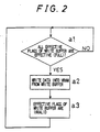
- Fig. 2 shows VRAM write timing according to the second embodiment of the invention.
- the access control circuit 13 makes a decision on whether or not all the effective flags 22 of the write buffer 15 are effective.
- the access control circuit 13 instructs the VRAM control circuit 18 to write data for the first time when the write buffer 15 is in a full state, and then, the write data is stored in the VRAM 20.
- software does not execute wasteful flow such that overwrite is continuously made on the same coordinate two times or more.
- the write buffer 15 becomes in a full state, in the next write data from the CPU 27, there is the high possibility that the high-order address of the write buffer 15 has been varied. Therefore, since there is no need of waiting for the timing of the writing operation from the write buffer 15 to the VRAM 20 any more, data is immediately written into the VRAM 20.
- step a2 VRAM writing is immediately executed when the write buffer 14 is in a full state, and in step a3, the effective flag 22 is kept invalid. By doing so, in the next write access from the CPU 27, even if effective write data is stored in the pre-buffer 12, it is possible to immediately transfer the write data to the write buffer 15, so that the write data can be immediately written into the pre-buffer 12 regardless of high-order address.
- Timing control of repeating processes from step a1 to step a3 is executed, and thereby, it is possible to capture write data without unnecessarily keeping the CPU 27 waiting. Therefore, this serves to achieve a speedup of the entirety of system into which the display memory control circuit 11 is incorporated.
- this timing control it is possible to store the most numerous CPU write data in the VRAM 20 by the least number of VRAM access times.
- This embodiment defines a data bus width of the CPU 27 as 8 bits and defines one address data width of the VRAM 20 as 128 bits.
- data equivalent to the maximum 16 times CPU access in the VRAM 20 is restricted to the minimum, so that a current consumption of the VRAM itself can be reduced.
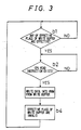
- VRAM write timing means control timing of first instructing the VRAM control circuit 18 to write data and storing the write data in the VRAM 20 in the case of reading a VRAM data from the CPU in a state that write data is stored in the pre-buffer 12 or the write buffer 15.
- step b1 waiting is made till any of effective flags 22 of the write buffer 15 is effective or the pre-effective flag 25 of the pre-buffer 12 is effective, that is, write data becomes in a state of being stored in the write buffer 15 or the pre-buffer 12.
- step b2 the sequence proceeds to step b3 in the case where the CPU 27 executes read access to the VRAM 20.
- this read access is still a read instruction to write data of VRAM address included in the write buffer 15, or write data of the pre-buffer 12.
- the write data is still not stored in the VRAM 20; for this reason, it is impossible to immediately read the write data from the VRAM 20.
- the access control circuit 13 instructs the VRAM control circuit 18 to immediately store write data stored in the pre-buffer 12 or the write buffer 15 in the VRAM 20. At this time, the access control circuit 13 outputs a wait signal to the CPU 27 at once so as to keep a time till read data is prepared.
- the write data of the pre-buffer 12 is transferred to the write buffer 15, and thereafter, the access control circuit 13 instructs the VRAM control circuit 18 to write the data of the write buffer 15 into the main body of VRAM 20.
- step b4 as soon as the pre-effective flag 25 of the pre-buffer 12 and all of the effective flags 22 of the write buffer 15 becomes invalid, the access control circuit 13 immediately instructs the VRAM control circuit 18 to read VRAM data of a specified address. And then, the read cycle controlled by the VRAM control circuit 18 ends, and thereafter, the access control circuit 13 outputs read data to the CPU 27, and cancels the wait signal. Data read from the VRAM 20 in the read cycle is temporarily stored in the data buffers 21 of the write buffer 15, and thereafter, is transmitted to the CPU 27 for each number of bits corresponding to data bus width. The read data does not always need to be stored in the data buffers 21 as described below.
- Fig. 4 shows VRAM access timing according to the fourth embodiment of the invention.
- a state that write data is stored in the write buffer 15 in the case where write data having of the same VRAM address is written in the VRAM from the CPU 27, by simultaneously writing the two write data together in the VRAM 20, it is possible to reduce the power consumption of the VRAM 20. Therefore, as described in the second embodiment shown in Fig. 2 , it is preferable to write the write data in the VRAM 20 after the write buffer 15 becomes in a full state.
- step c2 in order to solve the aforesaid problem, in the case where write data is stored in the write buffer 15 in step c1, after a predetermined time has elapsed in step c2, the access control circuit 13 executes a process for transferring the write data from the write buffer 15 to the VRAM 20. In step c4, the effective flag 22 of the write buffer 15 is made invalid, and the sequence returns to step c1.
- the time 19 is previously set so as to count a predetermined cycle time. If the preset time is too shorter, surplus VRAM accesses are executed. In this embodiment, in order to make full the write buffer 15 by the CPU 27, 16-bus cycle time of the CPU 27 is required. Thus, the preset cycle time should be at least longer than the 16-bus cycle time. After the given time elapsed, the access control circuit 13 instructs the VRAM timing control circuit 18 to write the write data of the write buffer 15 into the main body of VRAM 20.
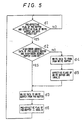
- Fig. 5 shows VRAM access timing according to the fifth embodiment of the invention.
- the access control circuit 13 in step d2, makes a comparison between a high-order address of the pre-address buffer 26 and a high-order address of the high-order address buffer 23 with the use of the high-order address comparator circuit 16.
- the write data stored in the pre-buffer 12 is identical to the VRAM address of the write data already existing in the write buffer 15; therefore, it is possible in step d3 to transfer the write data of the pre-buffer 12 to the write buffer 15.
- step d4 the access control circuit 13 immediately transfers the write data stored in the write buffer 15 to the VRAM 20, and then, in step d5, instructs the VRAM control circuit 18 to make invalid all the effective flags 22. Whereby the sequence proceeds to step d3, and it is possible to transfer the write data of the pre-buffer 12 to the write buffer 15.
- step d6 the pre-effective flag 25 of the pre-buffer 12 is made invalid so that new write data can be written, and the sequence returns to step d1.
- the aforesaid embodiments are applicable to a display device of an information processing apparatus with any of combinations.
- these embodiments of the invention are effectively applicable to the whole of portable appliances in which it is important to lower the amount of power consumption.
Landscapes
- Engineering & Computer Science (AREA)
- Physics & Mathematics (AREA)
- Computer Hardware Design (AREA)
- General Physics & Mathematics (AREA)
- Theoretical Computer Science (AREA)
- Multimedia (AREA)
- Controls And Circuits For Display Device (AREA)
- Control Of Indicators Other Than Cathode Ray Tubes (AREA)
- Memory System (AREA)
- Digital Computer Display Output (AREA)
Claims (5)
- Anzeigespeicher-Steuervorrichtung, die dazu ausgelegt ist, Daten in einen Anzeigespeicher (20), der eine Datenbusbreite besitzt, die eine mehrfache Datenbusbreite einer CPU (27) ist, zu schreiben, mit:einem Vorpuffer (12), der dazu ausgelegt ist, Adressen und Daten von der CPU (27) zu speichern, und dazu ausgelegt ist, einen Vorpuffereffektivmerker auszugeben, der als ein Signal verwendet wird, das angibt, ob im Vorpuffer Adressen und Daten gespeichert sind oder nicht;einem Schreibpuffer (15), der dazu ausgelegt ist, Daten mit derselben Anzahl von Bits wie die im Anzeigespeicher (20) gespeicherten Daten zu speichern, wobei der Schreibpuffer (15) in mehrere Bereiche unterteilt ist, wovon jeder die gleiche Anzahl von Bits wie die im Vorpuffer (12) gespeicherten Daten besitzt, wobei die Daten vom Vorpuffer (12) in einem dieser Bereiche gespeichert werden und wobei der Schreibpuffer (15) dazu ausgelegt ist, mehrere Effektivmerker auszugeben, die als ein Signal verwendet werden, das angibt, ob in den jeweiligen Bereichen effektive Daten gespeichert sind;einem Puffer (23) für Adressen hoher Ordnung, der dazu ausgelegt ist, eine Adresse hoher Ordnung, die einer vorgegebenen Anzahl von Bits entspricht, auf einer Seite hoher Ordnung von Adressdaten, die von dem Vorpuffer (12) ankommen, zu speichern;einem Decodierer (14) für Adressen niedriger Ordnung, der dazu ausgelegt ist, Adressen einer vorgegebenen Anzahl von Bits auf einer Seite niedriger Ordnung von Adressdaten, die von dem Vorpuffer (12) ankommen, zu decodieren;einer Komparatorschaltung (16) für Adressen hoher Ordnung, die dazu ausgelegt ist, einen Vergleich zwischen den Adressbits hoher Ordnung, die in dem Puffer (23) für Adressen hoher Ordnung gespeichert sind, und den Adressbits hoher Ordnung von Adressen in dem Vorpuffer (12) auszuführen;einer Zugriffssteuerschaltung (13), die dazu ausgelegt ist, eine Schreiboperation in den Schreibpuffer (15) zu steuern;einer Anzeigespeicher-Steuerschaltung (18), die dazu ausgelegt ist, die Lese- und Schreiboperationen des Anzeigespeichers über Datenbusse mit der gleichen Anzahl von Bits wie die Anzeigedaten zu steuern, undeiner Anzeigesteuerschaltung (17), die dazu ausgelegt ist, periodisch eine Leseoperation der Anzeigedaten von dem Anzeigespeicher (20) über die Anzeigespeicher-Steuerschaltung (18) auszuführen;wobei die Zugriffssteuerschaltung (13) auf den Vorpuffereffektivmerker und auf die Schreibpuffereffektivmerker Bezug nimmt und dazu ausgelegt ist, die in dem Vorpuffer (12) gespeicherten Daten in einen Bereich des Schreibpuf fers (15) zu schreiben, der anhand des Vergleichsergebnisses der Komparatorschaltung (16) für Adressen hoher Ordnung und eines decodierten Ausgangs des Decodierers (14) für Adressen niedriger Ordnung bestimmt wird, und dazu ausgelegt ist, die Anzeigespeicher-Steuerschaltung (18) zu steuern, um durch einen einmaligen Zugriff die in dem Schreibpuffer (15) gespeicherten Daten in den Anzeigespeicher (20) zu schreiben, falls wenigstens eine der folgenden Bedingungen (a) bis (d) erfüllt ist:(a) Fall, in dem die mehreren Effektivmerker des Schreibpuffers (15) alle das Vorhandensein von effektiven Daten angeben,(b) Fall, in dem in einem Zustand, in dem effektive Daten in dem Schreibpuffer (15) gespeichert sind, ein Lesebefehl für Speicherinhalte von der CPU (27) an den Anzeigespeicher (20) ausgegeben wird,(c) Fall, in dem nach einer gegebenen Zeitdauer effektive Daten in dem Schreibpuffer (15) gespeichert werden, und(d) Fall, in dem ein Ergebnis des Vergleichs der Komparatorschaltung (16) für Adressen hoher Ordnung angibt, dass Adressen hoher Ordnung nicht miteinander übereinstimmen, wenn sowohl der Effektivmerker des Schreibpuffers (15) als auch der Vorpuffereffektivmerker des Vorpuffers (12) angeben, dass effektive Daten vorhanden sind.
- Anzeigespeicher-Steuervorrichtung nach Anspruch 1, wobei die Zugriffssteuerschaltung (13) die Anzeigespeicher-Steuerschaltung (18) steuert, um Schreibdaten von dem Schreibpuffer (15) sofort in den Anzeigespeicher (20) zu schreiben, falls alle Effektivmerker des Schreibpuffers (15) das Vorhandensein effektiver Daten angeben.
- Anzeigespeicher-Steuervorrichtung nach Anspruch 1 oder 2, wobei die Zugriffssteuerschaltung (13) die Anzeigespeicher-Steuerschaltung (18) steuert, um Daten, die in dem Schreibpuffer (15) gespeichert sind, in den Anzeigespeicher (20) zu schreiben, falls in einem Zustand, in dem effektive Daten in dem Schreibpuffer (15) gespeichert sind, ein Lesebefehl für Speicherinhalte von der CPU (27) an den Anzeigespeicher (20) ausgegeben wird.
- Anzeigespeicher-Steuervorrichtung nach Anspruch 1 oder 2, wobei die Anzeigesteuervorrichtung ferner einen Zeitgeber (19) zum Zählen einer vorgegebene Zykluszeit enthält,
wobei die Zugriffssteuerschaltung (13) die Anzeigespeicher-Steuerschaltung (18) steuert, um Daten, die in dem Schreibpuffer (15) gespeichert sind, in den Anzeigespeicher (20) zu schreiben, falls in dem Schreibpuffer (15) effektive Daten gespeichert sind, wenn der Zeitgeber (19) eine gegebene Zeit zählt. - Anzeigespeicher-Steuervorrichtung nach Anspruch 1 oder 2, wobei die Zugriffssteuerschaltung (13) die Anzeigespeicher-Steuerschaltung (18) steuert, um Daten, die in dem Schreibpuffer (15) gespeichert sind, in den Anzeigespeicher (20) zu schreiben, falls in einem Zustand, in dem sowohl der Effektivmerker des Schreibpuffers (15) als auch der Vorpuffereffektivmerker des Vorpuffers (12) angeben, dass effektive Daten vorhanden sind, ein Ergebnis des Vergleichs der Komparatorschaltung (18) für Adressen hoher Ordnung angibt, dass Adressen hoher Ordnung nicht miteinander übereinstimmen.
Applications Claiming Priority (3)
| Application Number | Priority Date | Filing Date | Title |
|---|---|---|---|
| JP18006997 | 1997-07-04 | ||
| JP18006997A JP3342352B2 (ja) | 1997-07-04 | 1997-07-04 | 表示用メモリ制御装置 |
| JP180069/97 | 1997-07-04 |
Publications (3)
| Publication Number | Publication Date |
|---|---|
| EP0898264A2 EP0898264A2 (de) | 1999-02-24 |
| EP0898264A3 EP0898264A3 (de) | 2000-03-29 |
| EP0898264B1 true EP0898264B1 (de) | 2009-01-21 |
Family
ID=16076930
Family Applications (1)
| Application Number | Title | Priority Date | Filing Date |
|---|---|---|---|
| EP98112280A Expired - Lifetime EP0898264B1 (de) | 1997-07-04 | 1998-07-02 | Steuergerät für einen Videoanzeigespeicher |
Country Status (5)
| Country | Link |
|---|---|
| US (1) | US6278467B1 (de) |
| EP (1) | EP0898264B1 (de) |
| JP (1) | JP3342352B2 (de) |
| CN (1) | CN1109301C (de) |
| DE (1) | DE69840491D1 (de) |
Families Citing this family (8)
| Publication number | Priority date | Publication date | Assignee | Title |
|---|---|---|---|---|
| EP1160759A3 (de) * | 2000-05-31 | 2008-11-26 | Panasonic Corporation | Bildausgabevorrichtung und Verfahren zur Steuerung der Bildausgabe |
| EP1262939B1 (de) * | 2001-05-31 | 2012-02-01 | Nokia Corporation | Verfahren und Einrichtung zur Aktualisierung eines Bildspeichers mit reduzierter Leistungsaufnahme |
| JP2003281071A (ja) * | 2002-03-20 | 2003-10-03 | Seiko Epson Corp | データ転送制御装置、電子機器及びデータ転送制御方法 |
| JP4478001B2 (ja) * | 2004-12-03 | 2010-06-09 | 株式会社ソニー・コンピュータエンタテインメント | 画像表示装置、画像表示方法及びプログラム |
| CN101639931B (zh) * | 2008-07-30 | 2012-05-02 | 瑞鼎科技股份有限公司 | 存储器及像素数据储存方法 |
| US8602518B2 (en) * | 2010-04-06 | 2013-12-10 | Xerox Corporation | Test pattern effective for coarse registration of inkjet printheads and methods of analysis of image data corresponding to the test pattern in an inkjet printer |
| CN102103740B (zh) * | 2010-12-20 | 2013-01-02 | 福州瑞芯微电子有限公司 | 一种写入地址和宽度不对齐图像的处理方法和处理电路 |
| CN103077123A (zh) * | 2013-01-15 | 2013-05-01 | 华为技术有限公司 | 一种数据写入和读取方法及装置 |
Family Cites Families (9)
| Publication number | Priority date | Publication date | Assignee | Title |
|---|---|---|---|---|
| DE3015125A1 (de) | 1980-04-19 | 1981-10-22 | Ibm Deutschland Gmbh, 7000 Stuttgart | Einrichtung zur speicherung und darstellung graphischer information |
| EP0228745A3 (de) | 1985-12-30 | 1990-03-28 | Koninklijke Philips Electronics N.V. | Rasterabtastvideosteuergerät mit einem "Cache"-Speicher, Aktualisierungs-"Cache"-Speicher für ein solches Videosteuergerät und KSR-Anzeigeterminal mit einem solchen Videosteuergerät |
| JP3350043B2 (ja) * | 1990-07-27 | 2002-11-25 | 株式会社日立製作所 | 図形処理装置及び図形処理方法 |
| US5572655A (en) * | 1993-01-12 | 1996-11-05 | Lsi Logic Corporation | High-performance integrated bit-mapped graphics controller |
| JPH06332664A (ja) | 1993-03-23 | 1994-12-02 | Toshiba Corp | 表示制御システム |
| JPH0728990A (ja) | 1993-07-14 | 1995-01-31 | Nec Shizuoka Ltd | グラフィックスメモリアクセス回路 |
| JPH07319436A (ja) * | 1994-03-31 | 1995-12-08 | Mitsubishi Electric Corp | 半導体集積回路装置およびそれを用いた画像データ処理システム |
| US5625386A (en) * | 1994-09-30 | 1997-04-29 | Apple Computer, Inc. | Method and apparatus for interleaving display buffers |
| US5696947A (en) * | 1995-11-20 | 1997-12-09 | International Business Machines Corporation | Two dimensional frame buffer memory interface system and method of operation thereof |
-
1997
- 1997-07-04 JP JP18006997A patent/JP3342352B2/ja not_active Expired - Fee Related
-
1998
- 1998-07-01 US US09/108,807 patent/US6278467B1/en not_active Expired - Lifetime
- 1998-07-02 EP EP98112280A patent/EP0898264B1/de not_active Expired - Lifetime
- 1998-07-02 DE DE69840491T patent/DE69840491D1/de not_active Expired - Lifetime
- 1998-07-03 CN CN98115923A patent/CN1109301C/zh not_active Expired - Fee Related
Also Published As
| Publication number | Publication date |
|---|---|
| US6278467B1 (en) | 2001-08-21 |
| JP3342352B2 (ja) | 2002-11-05 |
| CN1204820A (zh) | 1999-01-13 |
| EP0898264A2 (de) | 1999-02-24 |
| CN1109301C (zh) | 2003-05-21 |
| EP0898264A3 (de) | 2000-03-29 |
| JPH1124644A (ja) | 1999-01-29 |
| DE69840491D1 (de) | 2009-03-12 |
Similar Documents
| Publication | Publication Date | Title |
|---|---|---|
| US5644784A (en) | Linear list based DMA control structure | |
| US6819334B1 (en) | Information processing apparatus and its display controller | |
| CN1105360C (zh) | 执行直接存储器访问(dma)字节交换的方法和装置 | |
| US6678755B1 (en) | Method and apparatus for appending memory commands during a direct memory access operation | |
| US6278467B1 (en) | Display memory control apparatus | |
| CN114785748B (zh) | 用于图像传输的dma控制系统与方法 | |
| CA2289192C (en) | Communication dma device | |
| US5471672A (en) | Method for implementing a high speed computer graphics bus | |
| JPH08278778A (ja) | 画像表示制御方法及び画像表示制御装置 | |
| US20030067456A1 (en) | Indirect interface | |
| JPH0696007A (ja) | Dma転送方式 | |
| JPH0431918A (ja) | キースキャン装置 | |
| JPS62183487A (ja) | ラスタ走査ビデオ制御装置 | |
| JPS5952460B2 (ja) | メモリ装置 | |
| JP2856244B2 (ja) | データ転送方式 | |
| JP3259095B2 (ja) | データ転送方法 | |
| JPH10254817A (ja) | Dma転送制御システム | |
| JPS63292355A (ja) | Dma転送制御方式 | |
| JPH11203232A (ja) | 情報処理装置および入出力制御装置 | |
| JPH0553548A (ja) | デイスプレイ制御装置 | |
| JPH0772837A (ja) | 表示システム | |
| JPS6029837A (ja) | 情報処理装置 | |
| JPH10240317A (ja) | モジュール装置 | |
| JPH06214749A (ja) | 描画制御装置 | |
| JPH0962562A (ja) | メモリの処理回路 |
Legal Events
| Date | Code | Title | Description |
|---|---|---|---|
| PUAI | Public reference made under article 153(3) epc to a published international application that has entered the european phase |
Free format text: ORIGINAL CODE: 0009012 |
|
| AK | Designated contracting states |
Kind code of ref document: A2 Designated state(s): DE FR GB |
|
| AX | Request for extension of the european patent |
Free format text: AL;LT;LV;MK;RO;SI |
|
| PUAL | Search report despatched |
Free format text: ORIGINAL CODE: 0009013 |
|
| AK | Designated contracting states |
Kind code of ref document: A3 Designated state(s): AT BE CH CY DE DK ES FI FR GB GR IE IT LI LU MC NL PT SE |
|
| AX | Request for extension of the european patent |
Free format text: AL;LT;LV;MK;RO;SI |
|
| 17P | Request for examination filed |
Effective date: 20000811 |
|
| AKX | Designation fees paid |
Free format text: DE FR GB |
|
| 17Q | First examination report despatched |
Effective date: 20070827 |
|
| GRAP | Despatch of communication of intention to grant a patent |
Free format text: ORIGINAL CODE: EPIDOSNIGR1 |
|
| GRAS | Grant fee paid |
Free format text: ORIGINAL CODE: EPIDOSNIGR3 |
|
| GRAA | (expected) grant |
Free format text: ORIGINAL CODE: 0009210 |
|
| AK | Designated contracting states |
Kind code of ref document: B1 Designated state(s): DE FR GB |
|
| REG | Reference to a national code |
Ref country code: GB Ref legal event code: FG4D |
|
| REF | Corresponds to: |
Ref document number: 69840491 Country of ref document: DE Date of ref document: 20090312 Kind code of ref document: P |
|
| PLBE | No opposition filed within time limit |
Free format text: ORIGINAL CODE: 0009261 |
|
| STAA | Information on the status of an ep patent application or granted ep patent |
Free format text: STATUS: NO OPPOSITION FILED WITHIN TIME LIMIT |
|
| 26N | No opposition filed |
Effective date: 20091022 |
|
| REG | Reference to a national code |
Ref country code: FR Ref legal event code: PLFP Year of fee payment: 18 |
|
| PGFP | Annual fee paid to national office [announced via postgrant information from national office to epo] |
Ref country code: FR Payment date: 20150626 Year of fee payment: 18 |
|
| PGFP | Annual fee paid to national office [announced via postgrant information from national office to epo] |
Ref country code: GB Payment date: 20150721 Year of fee payment: 18 Ref country code: DE Payment date: 20150721 Year of fee payment: 18 |
|
| REG | Reference to a national code |
Ref country code: DE Ref legal event code: R119 Ref document number: 69840491 Country of ref document: DE |
|
| GBPC | Gb: european patent ceased through non-payment of renewal fee |
Effective date: 20160702 |
|
| PG25 | Lapsed in a contracting state [announced via postgrant information from national office to epo] |
Ref country code: FR Free format text: LAPSE BECAUSE OF NON-PAYMENT OF DUE FEES Effective date: 20160801 Ref country code: DE Free format text: LAPSE BECAUSE OF NON-PAYMENT OF DUE FEES Effective date: 20170201 |
|
| REG | Reference to a national code |
Ref country code: FR Ref legal event code: ST Effective date: 20170331 |
|
| PG25 | Lapsed in a contracting state [announced via postgrant information from national office to epo] |
Ref country code: GB Free format text: LAPSE BECAUSE OF NON-PAYMENT OF DUE FEES Effective date: 20160702 |