EP0905764A2 - Méthode pour maximaliser le rendement de puces sur des tranches semi-conductrices - Google Patents
Méthode pour maximaliser le rendement de puces sur des tranches semi-conductrices Download PDFInfo
- Publication number
- EP0905764A2 EP0905764A2 EP98114247A EP98114247A EP0905764A2 EP 0905764 A2 EP0905764 A2 EP 0905764A2 EP 98114247 A EP98114247 A EP 98114247A EP 98114247 A EP98114247 A EP 98114247A EP 0905764 A2 EP0905764 A2 EP 0905764A2
- Authority
- EP
- European Patent Office
- Prior art keywords
- wafer
- chips
- yield
- center point
- wafer map
- Prior art date
- Legal status (The legal status is an assumption and is not a legal conclusion. Google has not performed a legal analysis and makes no representation as to the accuracy of the status listed.)
- Ceased
Links
Images


Classifications
-
- H—ELECTRICITY
- H10—SEMICONDUCTOR DEVICES; ELECTRIC SOLID-STATE DEVICES NOT OTHERWISE PROVIDED FOR
- H10P—GENERIC PROCESSES OR APPARATUS FOR THE MANUFACTURE OR TREATMENT OF DEVICES COVERED BY CLASS H10
- H10P74/00—Testing or measuring during manufacture or treatment of wafers, substrates or devices
- H10P74/23—Testing or measuring during manufacture or treatment of wafers, substrates or devices characterised by multiple measurements, corrections, marking or sorting processes
Definitions
- This disclosure relates to semiconductor wafers and more particularly, to a method of maximizing the overall yield of chips per wafer.
- Semiconductor crystal wafers such as those made of silicon, are used as a substrate for processing integrated circuit chips. As processing has improved over the years wafer diameters have increased to their current size of approximately 8 inches and greater. Wafers are generally sliced off from a large silicon crystal ingot and are therefore generally circular in shape.
- CMP Chemical mechanical polishing
- CMP is a process for improving the surface planarity of a semiconductor wafer and involves the use of mechanical pad polishing systems usually with a silica-based slurry.
- CMP offers a practical approach to achieving the important advantage of global wafer planarity.
- CMP systems for global planarization have certain limitations. These limitations include low wafer throughput, polished surface non-uniformity and a problem related to polishing uniformity known as "edge exclusion". Edge exclusion occurs when too much of the semiconductor wafer is polished. This causes the edge or outer portion of the wafer to be unusable for integrated circuit fabrication. Wafer polish throughput and polish uniformity are important process parameters, because they also directly affect the number of integrated circuit chips that a fabrication facility can produce for a given period of time.
- edge exclusions can be created by wafer handling devices.
- An edge exclusion can be defined on a given wafer by handling marks on that wafer. For example, a handling mark that extends further inward from the edge of the wafer than the polishing edge, defines the edge exclusion for that wafer. Edge exclusions tend to measure 2 to 8 millimeters radially outward from the innermost useable diameter to the edge of the wafer.
- a wafer map 20 is a layout of integrated circuit chips 12 on a wafer 18 which accounts for cuts between the chips as well.
- Wafer map 20 is fixed in defining the locations of individual chips 12 relative to one another.
- Wafer modeling programs are given a wafer map center point 16 and a given edge exclusion as input. The distance between point A and point B is the edge exclusion for wafer 18.
- An exclusion zone 14 is created at the outside of the wafer.
- a chip 12 that passes 3 mm past a diameter 22 is considered unusable.
- the wafer modeling program moves the wafer map by adjusting center point 16 within the region defined by diameter 22 until the maximum number of useable chips is achieved for a given edge exclusion.
- a method of fabricating semiconductor chips includes the steps of optimizing a number of chips that geometrically fit on a wafer and maximizing chip yield for the wafer by considering chips located in a normally rejectable location and utilizing yield probability data for the chip in the normally rejectable locations to weight the probability of an acceptable chip such that if the probability is above a threshold value the chips are not rejected. This results in an increased chip yield for semiconductor wafers.
- the step of optimizing a number of chips that geometrically fit on a wafer includes providing a predetermined wafer map for overlaying the wafer, the wafer map being referenced from a center point thereon and maximizing a first quantity of chips that can fit on the wafer by varying the center point of the wafer map on the wafer.
- the step of maximizing chip yield includes determining the quantity of chips that can fit on the wafer by varying an edge exclusion distance with a wafer map fixed at a maximized center point location, providing a yield probability curve for wafer map locations, multiplying the yield probability curve by the quantity of chips at each of the wafer map locations to obtain a weighted yield probability curve for each wafer map center point location, comparing alternative the weighted probability curves for different wafer map center point locations, and selecting the wafer map center point location to maximize the chip yield for the wafer.
- the steps of optimizing a number of chips that geometrically fit on a wafer and maximizing chip yield for the wafer may be performed by a computer.
- the present disclosure describes a method for maximizing the chip yield for a semiconductor wafer.
- yield probability data By introducing yield probability data into a wafer modeling program the number of usable chips can be increased for a wafer.
- the present method typically improves the yield in situations where an edge exclusion for a wafer is relatively larger.
- the method takes yield data collected for a given type of chip and weights the chip location on the wafer in accordance with the yield data. Since large edge exclusions equate to chips deemed unusable in the prior art technique, the weighting of yield probability saves some of these chips based on their location on the wafer. This results in a larger number of chips for a given wafer.
- FIG. 2 shows the number of integrated circuit chips that can be fabricated from a wafer.
- the wafer is an eight inch wafer, for example.
- the horizontal axis of FIG. 2 represents the edge exclusion dimension for a given chip in millimeters.
- the range of the horizontal axis can be, for example, between 2 mm and 8 mm. This range is determined by wafer map center point 16 (FIG. 1) which is limited in its displacement due to the geometries of wafer map 20 and wafer 18.
- FIG. 1 wafer map center point 16
- FIG. 2 is a plot of a curve 210 of a wafer modeler in which center point 16 of wafer map 20 was varied for a given edge exclusion until the maximum number of chips is determined. Generally, the variation shown in the maximum number of chips for a given edge exclusion decreases as the edge exclusion increases.
- corners 212 which are at the ends of horizontal line segments of curve 210.
- a horizontal line in FIG. 2 denotes no decrease in the number of chips for a given edge exclusion. This means that as the edge exclusion is increased the number of chips remains relatively constant over a given range of edge exclusion distance. This is typical for wafer modeling graphs which involve the circular geometry of the wafer and the rectangular shape of the chips. Several chips are deemed unusable simultaneously due to this geometrical mismatch. Referring to FIG. 1, as the edge exclusion distance (between point A and point B) is increased several chip corners, for example 12a, 12b and 12c, move deeper into exclusion zone 14 and are no longer deemed to be usable.
- FIG. 2 illustrates the prior art technique of maximizing the number of chips on a wafer. Based on FIG. 2, it appears as though point 1 with a smaller edge exclusion would result in a higher yield, for example, 146 chips.
- a left vertical axis of FIG. 3 shows the number of integrated circuit chips that can be fabricated from a wafer.
- the wafer is an eight inch wafer, for example.
- a horizontal axis of FIG. 3 represents the edge exclusion for a given chip in millimeters. The range of the horizontal axis can be between 2 mm and 8 mm as in FIG. 2.
- FIG. 3 illustrates the yield for a given edge exclusion when the center point of the wafer map is held fixed.
- a first curve 310 shows the chip yield per wafer over the range of edge exclusions with the center point fixed at the location determined by the wafer modeler for point 1 in FIG. 2.
- a second curve 312 shows the chip yield per wafer over the range of edge exclusions with the center point fixed at the location determined by the wafer modeler for point 2 in FIG. 2.
- Yield probability for an individual chip increases as the location of the chip is closer to the center of the wafer. This is illustrated by a curve 314.
- Curve 314 has a right vertical axis which denotes yield probability as a percent value. Curve 314 uses the same horizontal axis for edge exclusion as before. As illustrated by curve 314, yield probability increases for larger edge exclusions. Curve 314 is a typical yield probability curve for manufacturing chips. Despite the higher number of chips per wafer given initially for point 1 in FIG. 2, the wafer map center point may have moved more chips closer to the edge of a wafer thereby decreasing the number of usable chips due to their location on the wafer (increased distance from wafer center, therefore decreasing their yield probability).
- Curve 312 illustrates that for larger edge exclusions a plateau 316 remains constant over the illustrated range of edge exclusions. This signifies a potential advantage to replacing the center point of the wafer map from the location corresponding to point 1 (146 chips available) to the location corresponding to point 2 (140 chips available) in FIG. 2 for wafers with larger edge exclusions. This determination is based on the overall yield of the chips including those in exclusion zone 14 (FIG. 1) and not just geometrically fitting wafer map 20 on wafer 10 and eliminating those chips that fall into the exclusion zone.
- a method for incorporating yield probability into the placement of the wafer map includes obtaining wafer map center locations on a wafer by determining corner points 212 as illustrated in FIG.2. This is completed by assuming a value for an edge exclusion and varying the center of the wafer map to determine which location will allow the most chips to fit within the bounds of the edge exclusion based on geometry alone. This determination can be performed by an appropriately programmed computer.
- a corresponding center point 16 for the wafer map is determined.
- curve 310 and 312 of FIG. 3 are generated for the center points 16 corresponding to point 1 and point 2 of FIG. 2.
- the generation of curves 310 and 312 can be performed by an appropriately programmed computer.
- Curves 310 and 312 are generated by fixing the center point 16 location and varying the edge exclusion to determine the number of chips that can fit within the bounds of the edge exclusion as in FIG. 3.
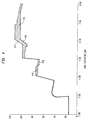
- Curves 310 and 312 (FIG. 3) are each multiplied by the yield probability curve 314 for the overall chip manufacturing process. Yield probability data at each edge exclusion dimension in FIG. 3 is multiplied by the corresponding value at the same edge exclusion value on the chips per wafer axis to obtain the plots shown in FIG. 4.
- a curve 410 is generated as a result of yield probability curve 314 and curve 310 multiplication.
- a curve 412 is generated in a similar way but by multiplying curve 314 by curve 312.
- a comparison may now be made between two alternative placements of wafer map center point 16 which includes the overall yield of the chips.
- the area under curve 410 and curve 412 is taken in the edge exclusion range between 2 mm and 8 mm, for example. The greater value of the area under each curve gives the most favorable yield probability.
- the generation of curves 410 and 412 can be performed by an appropriately programmed computer, and the areas under curves 410 and 412 can be computed using a numerical integration program, for example. In FIG.
- curve 412 gives a superior location for the center point of the wafer map. As graphically illustrated a region 414 and a region 416 exceed the area of region 418. Therefore, the location that would have been rejected in the prior art, for example point 2 of FIG. 1, provides a greater overall yield of usable chips since the location of the individual chips that would have been rejected may now be used based on the weight of the yield probability data which shows how successful a chip at a given location fares during acceptance testing.
- chip yield data is used to adjust for the weighting of the location of the wafer map. Yield increases can range for example, from 1-3% for wafer sizes of eight inches although higher yields are contemplated.
- a chip located at a position that was normally rejected due to its location in an exclusion zone of a wafer can now be considered for use based on the yield probability associated with its position on the wafer. If the yield probability for the chip at this location is above an assigned threshold value the chip can be accepted for use, hence increasing the overall yield for a given wafer.
Landscapes
- Testing Or Measuring Of Semiconductors Or The Like (AREA)
- Design And Manufacture Of Integrated Circuits (AREA)
- Die Bonding (AREA)
- Crystals, And After-Treatments Of Crystals (AREA)
Applications Claiming Priority (2)
| Application Number | Priority Date | Filing Date | Title |
|---|---|---|---|
| US08/937,764 US6070004A (en) | 1997-09-25 | 1997-09-25 | Method of maximizing chip yield for semiconductor wafers |
| US937764 | 1997-09-25 |
Publications (2)
| Publication Number | Publication Date |
|---|---|
| EP0905764A2 true EP0905764A2 (fr) | 1999-03-31 |
| EP0905764A3 EP0905764A3 (fr) | 1999-10-13 |
Family
ID=25470363
Family Applications (1)
| Application Number | Title | Priority Date | Filing Date |
|---|---|---|---|
| EP98114247A Ceased EP0905764A3 (fr) | 1997-09-25 | 1998-07-30 | Méthode pour maximaliser le rendement de puces sur des tranches semi-conductrices |
Country Status (6)
| Country | Link |
|---|---|
| US (1) | US6070004A (fr) |
| EP (1) | EP0905764A3 (fr) |
| JP (1) | JP4338240B2 (fr) |
| KR (1) | KR100562223B1 (fr) |
| CN (1) | CN1148784C (fr) |
| TW (1) | TW408348B (fr) |
Families Citing this family (19)
| Publication number | Priority date | Publication date | Assignee | Title |
|---|---|---|---|---|
| GB9812783D0 (en) | 1998-06-12 | 1998-08-12 | Cenes Ltd | High throuoghput screen |
| US6581202B1 (en) * | 2000-11-10 | 2003-06-17 | Viasystems Group, Inc. | System and method for monitoring and improving dimensional stability and registration accuracy of multi-layer PCB manufacture |
| KR100418194B1 (ko) * | 2001-04-07 | 2004-02-19 | 주식회사 메닉스 | 다이의 갯수를 최대화하는 방법 |
| US6823496B2 (en) | 2002-04-23 | 2004-11-23 | International Business Machines Corporation | Physical design characterization system |
| US6826738B2 (en) | 2002-05-10 | 2004-11-30 | Pdf Solutions, Inc. | Optimization of die placement on wafers |
| DE10243755B4 (de) * | 2002-09-20 | 2005-03-31 | Infineon Technologies Ag | Verfahren zum Bilden einer matrixförmigen Anordnung von Belichtungsfeldern auf einem idealisierten Halbleiterwafer |
| US7251743B2 (en) * | 2003-11-20 | 2007-07-31 | International Business Machines Corporation | Method, system, and program for transmitting input/output requests from a primary controller to a secondary controller |
| US7653523B2 (en) * | 2003-12-15 | 2010-01-26 | Lsi Corporation | Method for calculating high-resolution wafer parameter profiles |
| US7243325B2 (en) * | 2004-07-21 | 2007-07-10 | Bae Systems Information And Electronic Systems Integration Inc. | Method and apparatus for generating a wafer map |
| US7137098B2 (en) * | 2004-08-27 | 2006-11-14 | Lsi Logic Corporation | Pattern component analysis and manipulation |
| US7886238B1 (en) * | 2006-11-28 | 2011-02-08 | Cadence Design Systems, Inc. | Visual yield analysis of intergrated circuit layouts |
| JP2008156572A (ja) | 2006-12-26 | 2008-07-10 | Idemitsu Kosan Co Ltd | 樹脂用可塑剤およびそれを含む樹脂組成物 |
| CN101178745B (zh) * | 2007-11-16 | 2010-06-09 | 浙江大学 | 一种利用有效面积来建立记忆体电路的成品率模型的方法 |
| CN101183399B (zh) * | 2007-11-16 | 2010-12-08 | 浙江大学 | 一种分析和提高半导体生产线的成品率的方法 |
| CN101826123B (zh) * | 2010-01-29 | 2012-01-25 | 浙江大学 | 一种增加标准单元通孔提升芯片成品率的方法 |
| US8560980B2 (en) | 2010-11-16 | 2013-10-15 | International Business Machines Corporation | Optimal chip acceptance criterion and its applications |
| CN103164567A (zh) * | 2012-12-04 | 2013-06-19 | 天津蓝海微科技有限公司 | 一种根据流片数据拟合晶圆参数的方法 |
| US10290354B1 (en) * | 2017-10-31 | 2019-05-14 | Sandisk Technologies Llc | Partial memory die |
| CN111640647B (zh) * | 2019-12-19 | 2022-04-22 | 福建省晋华集成电路有限公司 | 芯片的排版方法 |
Family Cites Families (20)
| Publication number | Priority date | Publication date | Assignee | Title |
|---|---|---|---|---|
| US3751647A (en) * | 1971-09-22 | 1973-08-07 | Ibm | Semiconductor and integrated circuit device yield modeling |
| US3842491A (en) * | 1972-12-08 | 1974-10-22 | Ibm | Manufacture of assorted types of lsi devices on same wafer |
| JPS57143844A (en) * | 1981-02-28 | 1982-09-06 | Matsushita Electric Works Ltd | Chip composition of wafer |
| JPS58107633A (ja) * | 1981-12-21 | 1983-06-27 | Canon Inc | 特殊チツプを逃げたシヨツト配列方法 |
| JPS6347925A (ja) * | 1986-08-18 | 1988-02-29 | Oki Electric Ind Co Ltd | 半導体装置の製造方法 |
| US4841893A (en) * | 1988-03-18 | 1989-06-27 | Boat America Corporation | Boat fender |
| JPH03214764A (ja) * | 1990-01-19 | 1991-09-19 | Sharp Corp | 半導体チップの製造方法 |
| JPH043959A (ja) * | 1990-04-20 | 1992-01-08 | Seiko Epson Corp | 半導体集積回路 |
| US5578532A (en) * | 1990-07-16 | 1996-11-26 | Novellus Systems, Inc. | Wafer surface protection in a gas deposition process |
| US5620525A (en) * | 1990-07-16 | 1997-04-15 | Novellus Systems, Inc. | Apparatus for supporting a substrate and introducing gas flow doximate to an edge of the substrate |
| US5347465A (en) * | 1992-05-12 | 1994-09-13 | International Business Machines Corporation | Method of integrated circuit chips design |
| US5430734A (en) * | 1993-02-12 | 1995-07-04 | Metalithic Systems, Inc. | Fault-tolerant waferscale integrated circuit device and method |
| JPH07211622A (ja) * | 1994-01-27 | 1995-08-11 | Nikon Corp | 露光方法及び露光システム |
| US5609719A (en) * | 1994-11-03 | 1997-03-11 | Texas Instruments Incorporated | Method for performing chemical mechanical polish (CMP) of a wafer |
| JP3986571B2 (ja) * | 1994-12-09 | 2007-10-03 | 日本テキサス・インスツルメンツ株式会社 | 歩留り予測装置とその方法 |
| US5539652A (en) * | 1995-02-07 | 1996-07-23 | Hewlett-Packard Company | Method for manufacturing test simulation in electronic circuit design |
| US5699260A (en) * | 1995-03-14 | 1997-12-16 | Analog Devices, Incorporated | Technique for optimizing the number of IC chips obtainable from a wafer |
| JPH0927445A (ja) * | 1995-07-13 | 1997-01-28 | Nikon Corp | ショットマップ作成方法 |
| US5777901A (en) * | 1995-09-29 | 1998-07-07 | Advanced Micro Devices, Inc. | Method and system for automated die yield prediction in semiconductor manufacturing |
| IT1290887B1 (it) * | 1997-01-08 | 1998-12-14 | Consorzio Eagle | Procedimento per ottimizzare la fabbricazione di circuiti integrati |
-
1997
- 1997-09-25 US US08/937,764 patent/US6070004A/en not_active Expired - Lifetime
-
1998
- 1998-07-30 EP EP98114247A patent/EP0905764A3/fr not_active Ceased
- 1998-08-01 TW TW087112683A patent/TW408348B/zh not_active IP Right Cessation
- 1998-08-24 KR KR1019980034195A patent/KR100562223B1/ko not_active Expired - Fee Related
- 1998-09-18 CN CNB981196225A patent/CN1148784C/zh not_active Expired - Fee Related
- 1998-09-24 JP JP26992198A patent/JP4338240B2/ja not_active Expired - Fee Related
Also Published As
| Publication number | Publication date |
|---|---|
| CN1212453A (zh) | 1999-03-31 |
| EP0905764A3 (fr) | 1999-10-13 |
| CN1148784C (zh) | 2004-05-05 |
| KR19990029336A (ko) | 1999-04-26 |
| JPH11150045A (ja) | 1999-06-02 |
| JP4338240B2 (ja) | 2009-10-07 |
| KR100562223B1 (ko) | 2006-06-13 |
| TW408348B (en) | 2000-10-11 |
| US6070004A (en) | 2000-05-30 |
Similar Documents
| Publication | Publication Date | Title |
|---|---|---|
| US6070004A (en) | Method of maximizing chip yield for semiconductor wafers | |
| US7474386B2 (en) | Wafer flatness evaluation method, wafer flatness evaluation apparatus carrying out the evaluation method, wafer manufacturing method using the evaluation method, wafer quality assurance method using the evaluation method, semiconductor device manufacturing method using the evaluation method and semiconductor device manufacturing method using a wafer evaluated by the evaluation method | |
| US7704122B2 (en) | Customized polish pads for chemical mechanical planarization | |
| US6159075A (en) | Method and system for in-situ optimization for semiconductor wafers in a chemical mechanical polishing process | |
| Pei et al. | Fine grinding of silicon wafers: designed experiments | |
| US6828163B2 (en) | Wafer shape evaluating method and device producing method, wafer and wafer selecting method | |
| US7722436B2 (en) | Run-to-run control of backside pressure for CMP radial uniformity optimization based on center-to-edge model | |
| WO2001043194A1 (fr) | Procedes de remplissage au niveau de la grille permettant de reduire les effets de densite globale des motifs | |
| US6607423B1 (en) | Method for achieving a desired semiconductor wafer surface profile via selective polishing pad conditioning | |
| KR100239226B1 (ko) | 반도체 웨이퍼 연마 방법 및 그 연마패드 | |
| CN117140340A (zh) | 一种晶圆研磨控制方法、装置、设备及介质 | |
| CN114667594A (zh) | 晶片的研磨方法及硅晶片 | |
| US6682398B2 (en) | Method for characterizing the planarizing properties of an expendable material combination in a chemical-mechanical polishing process; simulation technique; and polishing technique | |
| HK1017142A (en) | Method of maximizing chip yield for semiconductor wafers | |
| US20020179941A1 (en) | Semiconductor device and method of manufacturing the same | |
| KR20060105855A (ko) | 반도체소자 제조를 위한 화학적기계적연마 방법 | |
| Bibby et al. | Cartesian coordinate maps for chemical mechanical planarization uniformity characterization | |
| EP1312112A2 (fr) | Procede de prevention des dommages aux tranches de silicium lors d'un processus sequentiel de polissage en plusieurs etapes | |
| US6495465B2 (en) | Method for appraising the condition of a semiconductor polishing cloth | |
| US20260070191A1 (en) | Abrasive conditioner and a method of fabricating the same | |
| JP2000216116A (ja) | 高平坦度ウェ―ハの再加工方法 | |
| Zhang et al. | Mapping wafer flatness changes in chemical mechanical planarization | |
| JPH02121897A (ja) | 薄膜磁気トランスデューサの製造方法 |
Legal Events
| Date | Code | Title | Description |
|---|---|---|---|
| PUAI | Public reference made under article 153(3) epc to a published international application that has entered the european phase |
Free format text: ORIGINAL CODE: 0009012 |
|
| AK | Designated contracting states |
Kind code of ref document: A2 Designated state(s): DE FR GB IE IT NL |
|
| AX | Request for extension of the european patent |
Free format text: AL;LT;LV;MK;RO;SI |
|
| PUAL | Search report despatched |
Free format text: ORIGINAL CODE: 0009013 |
|
| AK | Designated contracting states |
Kind code of ref document: A3 Designated state(s): AT BE CH CY DE DK ES FI FR GB GR IE IT LI LU MC NL PT SE |
|
| AX | Request for extension of the european patent |
Free format text: AL;LT;LV;MK;RO;SI |
|
| 17P | Request for examination filed |
Effective date: 19991208 |
|
| AKX | Designation fees paid |
Free format text: DE FR GB IE IT NL |
|
| RAP1 | Party data changed (applicant data changed or rights of an application transferred) |
Owner name: INFINEON TECHNOLOGIES AG |
|
| REG | Reference to a national code |
Ref country code: HK Ref legal event code: WD Ref document number: 1017142 Country of ref document: HK |
|
| RAP1 | Party data changed (applicant data changed or rights of an application transferred) |
Owner name: INFINEON TECHNOLOGIES AG |
|
| RAP1 | Party data changed (applicant data changed or rights of an application transferred) |
Owner name: QIMONDA AG |
|
| STAA | Information on the status of an ep patent application or granted ep patent |
Free format text: STATUS: THE APPLICATION HAS BEEN REFUSED |
|
| 18R | Application refused |
Effective date: 20110227 |