EP0908947A2 - Procédé de fabrication d'un dispositif semi-conducteur avec un transistor pMIS - Google Patents
Procédé de fabrication d'un dispositif semi-conducteur avec un transistor pMIS Download PDFInfo
- Publication number
- EP0908947A2 EP0908947A2 EP98118296A EP98118296A EP0908947A2 EP 0908947 A2 EP0908947 A2 EP 0908947A2 EP 98118296 A EP98118296 A EP 98118296A EP 98118296 A EP98118296 A EP 98118296A EP 0908947 A2 EP0908947 A2 EP 0908947A2
- Authority
- EP
- European Patent Office
- Prior art keywords
- gate electrode
- transistor
- fluorine
- gate
- forming
- Prior art date
- Legal status (The legal status is an assumption and is not a legal conclusion. Google has not performed a legal analysis and makes no representation as to the accuracy of the status listed.)
- Withdrawn
Links
- 238000000034 method Methods 0.000 title claims description 108
- 239000004065 semiconductor Substances 0.000 title claims description 75
- 229910052731 fluorine Inorganic materials 0.000 claims abstract description 104
- 239000011737 fluorine Substances 0.000 claims abstract description 104
- 239000000758 substrate Substances 0.000 claims abstract description 70
- 229910052796 boron Inorganic materials 0.000 claims abstract description 34
- ZOXJGFHDIHLPTG-UHFFFAOYSA-N Boron Chemical compound [B] ZOXJGFHDIHLPTG-UHFFFAOYSA-N 0.000 claims abstract description 25
- 238000000059 patterning Methods 0.000 claims abstract description 7
- 239000012535 impurity Substances 0.000 claims description 46
- 150000002500 ions Chemical class 0.000 claims description 34
- 229910015900 BF3 Inorganic materials 0.000 claims description 24
- WTEOIRVLGSZEPR-UHFFFAOYSA-N boron trifluoride Chemical compound FB(F)F WTEOIRVLGSZEPR-UHFFFAOYSA-N 0.000 claims description 17
- 238000005468 ion implantation Methods 0.000 claims description 16
- 238000010438 heat treatment Methods 0.000 claims description 12
- 239000012212 insulator Substances 0.000 claims description 11
- 230000001681 protective effect Effects 0.000 claims description 8
- PXGOKWXKJXAPGV-UHFFFAOYSA-N Fluorine Chemical compound FF PXGOKWXKJXAPGV-UHFFFAOYSA-N 0.000 claims 12
- FGUUSXIOTUKUDN-IBGZPJMESA-N C1(=CC=CC=C1)N1C2=C(NC([C@H](C1)NC=1OC(=NN=1)C1=CC=CC=C1)=O)C=CC=C2 Chemical compound C1(=CC=CC=C1)N1C2=C(NC([C@H](C1)NC=1OC(=NN=1)C1=CC=CC=C1)=O)C=CC=C2 FGUUSXIOTUKUDN-IBGZPJMESA-N 0.000 claims 1
- -1 fluorine ions Chemical class 0.000 abstract description 61
- YCKRFDGAMUMZLT-UHFFFAOYSA-N Fluorine atom Chemical compound [F] YCKRFDGAMUMZLT-UHFFFAOYSA-N 0.000 abstract description 49
- 229910021420 polycrystalline silicon Inorganic materials 0.000 abstract description 27
- XUIMIQQOPSSXEZ-UHFFFAOYSA-N Silicon Chemical compound [Si] XUIMIQQOPSSXEZ-UHFFFAOYSA-N 0.000 abstract description 18
- 229910052710 silicon Inorganic materials 0.000 abstract description 18
- 239000010703 silicon Substances 0.000 abstract description 18
- 238000004151 rapid thermal annealing Methods 0.000 abstract description 13
- VYPSYNLAJGMNEJ-UHFFFAOYSA-N Silicium dioxide Chemical compound O=[Si]=O VYPSYNLAJGMNEJ-UHFFFAOYSA-N 0.000 abstract description 12
- 235000012239 silicon dioxide Nutrition 0.000 abstract description 6
- 239000000377 silicon dioxide Substances 0.000 abstract description 6
- 239000007943 implant Substances 0.000 description 15
- 229920002120 photoresistant polymer Polymers 0.000 description 11
- 238000009792 diffusion process Methods 0.000 description 8
- 230000000694 effects Effects 0.000 description 8
- ZAMOUSCENKQFHK-UHFFFAOYSA-N Chlorine atom Chemical compound [Cl] ZAMOUSCENKQFHK-UHFFFAOYSA-N 0.000 description 7
- UFHFLCQGNIYNRP-UHFFFAOYSA-N Hydrogen Chemical compound [H][H] UFHFLCQGNIYNRP-UHFFFAOYSA-N 0.000 description 7
- 230000015556 catabolic process Effects 0.000 description 7
- 239000000460 chlorine Substances 0.000 description 7
- 229910052801 chlorine Inorganic materials 0.000 description 7
- 239000001257 hydrogen Substances 0.000 description 7
- 229910052739 hydrogen Inorganic materials 0.000 description 7
- 238000002513 implantation Methods 0.000 description 7
- 229910052785 arsenic Inorganic materials 0.000 description 6
- RQNWIZPPADIBDY-UHFFFAOYSA-N arsenic atom Chemical compound [As] RQNWIZPPADIBDY-UHFFFAOYSA-N 0.000 description 5
- 238000005516 engineering process Methods 0.000 description 4
- 238000002955 isolation Methods 0.000 description 4
- 238000004519 manufacturing process Methods 0.000 description 3
- 150000004767 nitrides Chemical class 0.000 description 3
- 230000001133 acceleration Effects 0.000 description 2
- 238000009825 accumulation Methods 0.000 description 2
- 230000015572 biosynthetic process Effects 0.000 description 2
- BPUBBGLMJRNUCC-UHFFFAOYSA-N oxygen(2-);tantalum(5+) Chemical compound [O-2].[O-2].[O-2].[O-2].[O-2].[Ta+5].[Ta+5] BPUBBGLMJRNUCC-UHFFFAOYSA-N 0.000 description 2
- 230000001737 promoting effect Effects 0.000 description 2
- 229910001936 tantalum oxide Inorganic materials 0.000 description 2
- OAICVXFJPJFONN-UHFFFAOYSA-N Phosphorus Chemical compound [P] OAICVXFJPJFONN-UHFFFAOYSA-N 0.000 description 1
- 230000002411 adverse Effects 0.000 description 1
- 230000005465 channeling Effects 0.000 description 1
- 230000000295 complement effect Effects 0.000 description 1
- 239000013078 crystal Substances 0.000 description 1
- 230000007423 decrease Effects 0.000 description 1
- 230000006866 deterioration Effects 0.000 description 1
- 230000002542 deteriorative effect Effects 0.000 description 1
- 238000002474 experimental method Methods 0.000 description 1
- 125000001153 fluoro group Chemical group F* 0.000 description 1
- 239000007789 gas Substances 0.000 description 1
- 238000009413 insulation Methods 0.000 description 1
- 229910052698 phosphorus Inorganic materials 0.000 description 1
- 239000011574 phosphorus Substances 0.000 description 1
Images




Classifications
-
- H—ELECTRICITY
- H10—SEMICONDUCTOR DEVICES; ELECTRIC SOLID-STATE DEVICES NOT OTHERWISE PROVIDED FOR
- H10D—INORGANIC ELECTRIC SEMICONDUCTOR DEVICES
- H10D84/00—Integrated devices formed in or on semiconductor substrates that comprise only semiconducting layers, e.g. on Si wafers or on GaAs-on-Si wafers
- H10D84/01—Manufacture or treatment
- H10D84/0123—Integrating together multiple components covered by H10D12/00 or H10D30/00, e.g. integrating multiple IGBTs
- H10D84/0126—Integrating together multiple components covered by H10D12/00 or H10D30/00, e.g. integrating multiple IGBTs the components including insulated gates, e.g. IGFETs
- H10D84/0165—Integrating together multiple components covered by H10D12/00 or H10D30/00, e.g. integrating multiple IGBTs the components including insulated gates, e.g. IGFETs the components including complementary IGFETs, e.g. CMOS devices
- H10D84/0181—Manufacturing their gate insulating layers
-
- H—ELECTRICITY
- H10—SEMICONDUCTOR DEVICES; ELECTRIC SOLID-STATE DEVICES NOT OTHERWISE PROVIDED FOR
- H10D—INORGANIC ELECTRIC SEMICONDUCTOR DEVICES
- H10D84/00—Integrated devices formed in or on semiconductor substrates that comprise only semiconducting layers, e.g. on Si wafers or on GaAs-on-Si wafers
- H10D84/01—Manufacture or treatment
- H10D84/02—Manufacture or treatment characterised by using material-based technologies
- H10D84/03—Manufacture or treatment characterised by using material-based technologies using Group IV technology, e.g. silicon technology or silicon-carbide [SiC] technology
- H10D84/038—Manufacture or treatment characterised by using material-based technologies using Group IV technology, e.g. silicon technology or silicon-carbide [SiC] technology using silicon technology, e.g. SiGe
Definitions
- the present invention relates to an improved method for fabricating a semiconductor device including a highly reliable pMIS transistor with physical stress on the gate insulating film thereof reduced.
- the thickness of the gate insulating film thereof has also been reduced.
- a very thin gate insulating film is provided to have a thickness of several nm or less, then the reliability of the gate insulating film is deteriorated. This is because the physical stress applied on the gate insulating film cannot be sufficiently reduced owing to the difference between the thermal expansion coefficient of a gate electrode and that of the gate insulating film. Accordingly, it is widely recognized that technology for improving the reliability of a gate insulating film plays a significant role in implementing such a thin gate insulating film.
- FIGS 8(a) through 8(d) are cross-sectional views illustrating an extract of the process steps for fabricating a pMOS transistor as disclosed in Figures 3(a) through 3(i) of the publication.
- a gate insulating film 102 and a gate electrode 103 are formed on an n-type semiconductor layer (silicon substrate) 101 , and boron (B + ) ions are implanted into the entire substrate, thereby forming a p + layer 104 .
- fluorine (F + ) ions are implanted at a certain tilt angle on the conditions that the acceleration voltage is set at 40 keV and the dose is set at 1 ⁇ 10 14 cm -2 . Thereafter, heat treatment is conducted to diffuse boron ions, thereby turning the major part of the gate electrode 103 into a p-type region and turning the side portions of the gate electrode 103 into a high-resistance layer 112 .
- the p + layer 104 is turned into a p layer 106 and an end layer (fluorine-doped layer) 113 is formed to surround the p layer 106 .
- insulator sidewalls 107 are formed on the side surfaces of the gate electrode 103 .
- boron fluoride (BF 2 + ) ions are implanted on the conditions that the acceleration voltage is set in the range from 30 keV to 50 keV and the dose is set in the range from 1 ⁇ 10 15 cm -2 to 1 ⁇ 10 16 cm -2 and then heat treatment is conducted, thereby forming a highly-doped source region 109 , a highly-doped drain region 110 , a lightly-doped layer 108 (parts of the p layer 106 ) as a so-called LDD layer and the end layer 113 .
- boron fluoride (BF 2 + ) ions are implanted on the conditions that the acceleration voltage is set in the range from 30 keV to 50 keV and the dose is set in the range from 1 ⁇ 10 15 cm -2 to 1 ⁇ 10 16 cm -2 and then heat treatment is conducted, thereby forming a highly-doped source region 109 , a highly-doped drain region 110 , a lightly-doped layer
- a pMOS transistor having such a structure by promoting the diffusion of boron ions in the gate electrode 103 with the implantation of fluorine ions, fluorine ions can be doped into the gate insulating film 102 at a high doping level. As a result, the stress applied into the gate insulating film 102 owing the difference between the thermal expansion coefficient of the gate electrode 103 and that of the gate insulating film 102 can be reduced. In addition, since fluorine ions have been doped into the substrate, the diffusion of boron ions can be suppressed and therefore a shallow junction can be formed. It is noted that the high-resistance layer 112 is formed in the gate electrode 103 in order to increase the breakdown voltage thereof.
- boron ions diffusing in the gate electrode, are likely to enter the substrate. That is to say, a "boron passage" phenomenon happens and adversely varies the threshold voltage of a pMIS transistor from a predetermined value. Specifically, boron ions, which have been implanted into the gate electrode of a pMIS transistor, are likely to pass through a thin gate insulating film to diffuse into the substrate during a subsequent heat treatment.
- the variation in threshold voltages of a pMIS transistor also causes various problems in a so-called “dual-gate-type semiconductor device", in which a gate electrode made of n + -type polycrystalline silicon and a gate electrode made of p + -type polycrystalline silicon are used for nMIS and pMIS transistors, respectively.
- the reliability of a gate insulating film is disadvantageously deteriorated because of the accumulation of boron ions in the gate insulating film.
- the reliability of a gate insulating film is allegedly improved by reducing the stress applied into the gate insulating film through the introduction of fluorine ions into the gate insulating film.
- the reliability of the gate insulating film is still deteriorated because of a different reason, i.e., not only fluorine ions but also boron ions enter the gate insulating film.
- the present invention was made to accomplish the object of providing a method for fabricating a semiconductor device that can improve the reliability of a gate insulating film and prevent the characteristics of a pMIS transistor from varying by modifying the conditions on which fluorine ions are implanted into a gate electrode.
- a first method for fabricating a semiconductor device includes the steps of: a) sequentially forming a gate insulating film and a semiconductor film over a region of a semiconductor substrate where a pMIS transistor is to be formed; b) forming a gate electrode for the pMIS transistor by patterning the semiconductor film; c) introducing an impurity containing fluorine into the gate electrode of the pMIS transistor in accordance with ion implantation technique such that the dose of fluorine is in the range from 2 ⁇ 10 13 cm -2 to 2 ⁇ 10 15 cm -2 before or after the step b) is performed; d) introducing boron into the gate electrode of the pMIS transistor; e) forming source/drain regions for the pMIS transistor by introducing a p-type impurity into the semiconductor substrate; and f) diffusing fluorine in the gate electrode to the gate insulating film by conducting a heat treatment.
- a pMIS transistor formed in accordance with this method has advantageous characteristics as follows.
- fluorine is introduced into the gate insulating film of the pMIS transistor in the step c)
- the physical stress applied on the gate insulating film because of the difference between the thermal expansion coefficient of the gate electrode and that of the gate insulating film can be reduced.
- the reliability of the transistor can be improved.
- fluorine is also introduced into the gate electrode in accordance with ion implantation technique at a dose in the range from 2 ⁇ 10 13 cm -2 to 2 ⁇ 10 15 cm -2 , it is possible to prevent boron, which is introduced into the gate electrode in the step d), from entering the gate insulating film and the semiconductor substrate.
- boron which is introduced into the gate electrode in the step d
- the step c) may be performed to introduce the impurity containing fluorine into the entire surface of the semiconductor film after the step a) has been performed and before the step b) is performed.
- the steps c) and d) may be performed simultaneously by introducing boron fluoride as the impurity containing fluorine into the entire surface of the semiconductor film after the step a) has been performed and before the step b) is performed.
- the method may further include the step of forming a protective insulating film over the semiconductor film after the steps c) and d) have been performed.
- the step b) not only the gate electrode but also the protective insulating film may be patterned.
- the step e) may be performed by implanting p-type impurity ions with the gate electrode, covered with the protective insulating film, used as a mask. Then, the doping level of boron in the gate electrode and that of the p-type impurity in the source/drain regions in the semiconductor substrate can be independently controlled at respectively appropriate values.
- the steps c) and d) may be performed simultaneously by introducing boron fluoride as the impurity containing fluorine.
- the process can be simplified.
- the step c) may be performed to introduce the impurity containing fluorine into the gate electrode and the semiconductor substrate after the step b) has been performed.
- the step c) since the diffusion of boron in the semiconductor substrate can be suppressed, a shallow junction can be formed easily.
- the step c) may be performed by implanting ions of single-element fluorine.
- the steps d) and e) may be performed by introducing single-element boron into the semiconductor substrate with the gate electrode used as a mask after the step b) has been performed. Then, the doping levels of fluorine and boron can be independently controlled at respectively appropriate values.
- the impurity containing fluorine is more preferably introduced in accordance with ion implantation technique such that the dose of fluorine is 2 ⁇ 10 14 cm -2 or more.
- the method preferably further includes, prior to the step e), the steps of: forming an LDD region for the pMIS transistor by introducing a p-type impurity into the semiconductor substrate with the gate electrode used as a mask, and forming insulator sidewalls on side surfaces of the gate electrode of the pMIS transistor.
- the step e) is preferably performed by using the insulator sidewalls and the gate electrode as a mask. In such an embodiment, a highly reliable pMIS transistor having stable characteristics can be obtained even though the transistor has a so-called "LDD structure".
- the gate insulating film and the semiconductor film may be formed so as to also cover a region of the semiconductor substrate where an nMIS transistor is to be formed.
- a gate electrode for the nMIS transistor may be formed by patterning the semiconductor film.
- the impurity containing fluorine may also be introduced in accordance with ion implantation technique into the gate electrode of the nMIS transistor.
- the method may further include the step of forming source/drain regions for the nMIS transistor by introducing an n-type impurity into the region of the semiconductor substrate where the nMIS transistor is to be formed with the gate electrode for the nMIS transistor used as a mask. In such an embodiment, a complementary MIS transistor is formed. Since fluorine is also introduced into the gate insulating film of the nMIS transistor, the reliability of the nMIS transistor is also improved because of the above-described functions.
- a second method for fabricating a semiconductor device includes the steps of: a) sequentially forming a gate insulating film and a semiconductor film over respective regions of a semiconductor substrate where nMIS and pMIS transistors are to be formed; b) forming respective gate electrodes for the nMIS and the pMIS transistors by patterning the semiconductor film; c) forming p-type lightly-doped source/drain regions in the region where the pMIS transistor is to be formed by introducing boron fluoride into the gate electrodes and the entire semiconductor substrate in accordance with ion implantation technique after the step b) has been performed; d) forming n-type lightly-doped source/drain regions in the region of the semiconductor substrate where the nMIS transistor is to be formed by introducing an n-type impurity at a level higher than that of boron fluoride; e) forming insulator sidewalls on side surfaces of each said gate electrode; f) forming p-type highly-d
- a semiconductor device including highly reliable pMIS and nMIS transistors with stable characteristics can be obtained, even though the pMIS and nMIS transistors both have a so-called "LDD structure".
- the introduction of fluorine into the gate electrode and the formation of an LDD region in the pMIS transistor are simultaneously performed during a single process step, the number of process steps and the fabrication costs of a semiconductor device can both be reduced.
- Figures 1(a) through 1(e) are cross-sectional views illustrating a method for fabricating a semiconductor device in the first embodiment of the present invention.
- an n-well 1A and a p-well 1B are formed in respective regions Rp and Rn of a silicon substrate 1 where pMOS and nMOS transistors are to be formed.
- these regions will be referred to as “pMOS transistor forming region” and “nMOS transistor forming region”.
- an element isolation region 5 is formed to electrically isolate these regions from each other.
- a gate oxide film 2 made of silicon dioxide having a thickness of 5 nm, is formed over the silicon substrate 1 and a polycrystalline silicon film 3 having a thickness of 200 nm is deposited thereon.
- fluorine ions are implanted into the entire polycrystalline silicon film 3 on the conditions that the implant energy is set at 10 keV and the dose is set at 5 ⁇ 10 14 cm -2 .
- the polycrystalline silicon film 3 and the gate oxide film 2 are patterned, thereby forming gate electrode 3A , 3B and gate oxide films 2A , 2B for the pMOS and nMOS transistors, respectively. It is noted that the gate oxide film 2 is not necessarily patterned.
- the n-type doped layer 7 is formed by implanting n-type impurity ions such as arsenic (As) into the nMOS transistor forming region Rn at an angle substantially vertical to the surface of the substrate on the conditions that the implant energy is set at 30 keV and the dose is set at 2 ⁇ 10 15 cm -2 with the pMOS transistor forming region Rp covered with a photoresist mask or the like.
- the conductivity type of the gate electrode 3B in the nMOS transistor forming region Rn is also turned into n-type. That is to say, the polycrystalline silicon film 3 is turned into an n-type polycrystalline silicon film.
- the p-type doped layer 8 is formed by implanting p-type impurity ions such as boron (B) into the pMOS transistor forming region Rp at an angle substantially vertical to the surface of the substrate on the conditions that the implant energy is set at 8 keV and the dose is set at 2 ⁇ 10 15 cm -2 with the nMOS transistor forming region Rn covered with a photoresist mask or the like.
- the conductivity type of the gate electrode 3A in the pMOS transistor forming region Rp is also turned into p-type. That is to say, the polycrystalline silicon film 3 is turned into a p-type polycrystalline silicon film.
- the ion implantation at the "angle substantially vertical to the surface of the substrate” is performed at a tilt angle of about 7 degrees for preventing channeling. It is noted that though the angle is vertical to the surface of the substrate in the cross section (shown in Figure 1(e) ) including the channel direction of the gate electrodes, the angle is tilted 7 degrees with respect to the surface of the substrate in a cross section parallel to the gate width direction.
- fluorine ions are first introduced into the polycrystalline silicon film 3 to be the gate electrodes 3A and 3B . And after the gate electrodes 3A and 3B have been formed, a heat treatment is conducted, thereby diffusing fluorine ions from the gate electrodes 3A and 3B into the gate oxide films 2A and 2B , respectively.
- the physical stress applied on the gate oxide films 2A and 2B because of the difference between the thermal expansion coefficient of the gate electrodes 3A , 3B and that of the gate oxide films 2A , 2B can be reduced in the nMOS and pMOS transistors. As a result, the reliability of the gate oxide films 2A and 2B can be improved.
- fluorine ions are implanted at an appropriate dose of 5 ⁇ 10 14 cm -2 , and it is possible to prevent boron, which has been introduced into the gate electrode 3A of the pMOS transistor, from passing through the gate oxide film 2A to enter the silicon substrate 1 . That is to say, the variation in characteristics of the pMOS transistor can be suppressed.
- fluorine ions are implanted in the process step shown in Figure 1(c) .
- fluorine may be naturally introduced into the gate electrode 3A by implanting any other impurity ions, such as BF 2 + , containing fluorine.
- the implant dose of the impurity may be set at an arbitrary value so long as the dose of fluorine atoms, derived by converting the dose of the impurity introduced, falls within the above-described range (from 2 ⁇ 10 13 cm -2 to 2 ⁇ 10 15 cm -2 ).
- the implant energy may also be set at an arbitrary value so long as the impurity does not pass through the gate electrode during the ion implantation.
- the specific energy value is variable depending on the thickness of the gate electrode. In general, the energy may be 15 keV to 20 keV or less.
- Hydrogen or chlorine may be introduced through the implantation of some impurity containing hydrogen or chlorine or the diffusion resulting from a heat treatment in a gas containing hydrogen or chlorine.
- the doping levels of boron in the gate electrodes 3A and 3B and in the silicon substrate 1 can be advantageously controlled independently at respectively appropriate values.
- a dual-gate-type cMOS transistor may be formed by performing independent ion implantation processes using masks in such a manner that boron is introduced into the polycrystalline silicon film 3 in the pMOS transistor forming region Rp and that phosphorus or arsenic is introduced into the polycrystalline silicon film 3 in the nMOS transistor forming region Rn .
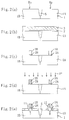
- Figures 2(a) through 2(e) are cross-sectional views illustrating a method for fabricating a semiconductor device in the second embodiment of the present invention.
- an n-well 1A and a p-well 1B are formed as in the first embodiment in the pMOS transistor forming region Rp and the nMOS transistor forming region Rn of a silicon substrate 1 , respectively. Then, an element isolation region 5 is formed to electrically isolate these regions from each other.
- a gate oxide film 2 having a thickness of 5 nm, is formed over the silicon substrate 1 and a polycrystalline silicon film 3 having a thickness of 200 nm is deposited thereon.
- the polycrystalline silicon film 3 and the gate oxide film 2 are patterned, thereby forming gate electrodes 3A , 3B and gate oxide films 2A , 2B for the pMOS and nMOS transistors, respectively. It is noted that the gate oxide film 2 is not necessarily patterned.
- fluorine ions are implanted into the entire substrate at an angle substantially vertical to the surface of the substrate on the conditions that the implant energy is set at 10 keV and the dose is set at 5 ⁇ 10 14 cm -2 .
- sidewalls 11 made of silicon dioxide, are formed on the side surfaces of each gate electrode 3A , 3B as in the first embodiment.
- n-type and p-type doped layers 7 and 8 which are to constitute respective source/drain regions for the nMOS and pMOS transistors, are formed.
- rapid thermal annealing is conducted at 1000°C for 10 seconds, thereby completing the pMOS and nMOS transistors.
- fluorine diffuses from the gate electrodes 3A , 3B into the gate oxide films 2A , 2B .
- n-type and p-type doped layers 7 and 8 are formed in the same way as in the first embodiment.
- fluorine ions are implanted after the gate electrodes 3A and 3B have been formed and before the impurity for forming the n-type and p-type doped layers 7 and 8 is implanted.
- fluorine ions may be implanted after the impurity for forming the n-type and p-type doped layers 7 and 8 has been implanted. In such a case, rapid thermal annealing is conducted after fluorine ions have been implanted.
- impurity ions containing fluorine may be implanted in place of fluorine ions.
- the dose thereof may be set at such a value as suppressing the passage of boron through the pMOS transistor.
- the physical stress on the gate oxide films 2A and 2B can also be reduced and the reliability of the gate oxide films 2A and 2B can also be improved.
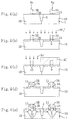
- Figures 3(a) through 3(e) are cross-sectional views illustrating a method for fabricating a semiconductor device in the third embodiment of the present invention.
- an n-well 1A and a p-well 1B are formed as in the first embodiment in the pMOS transistor forming region Rp and the nMOS transistor forming region Rn of a silicon substrate 1 , respectively. Then, an element isolation region 5 is formed to electrically isolate these regions from each other. Next, a gate oxide film 2 , having a thickness of 5 nm, is formed over the silicon substrate 1 and a polycrystalline silicon film 3 having a thickness of 200 nm is deposited thereon.
- the polycrystalline silicon film 3 and the gate oxide film 2 are patterned, thereby forming gate electrodes 3A , 3B and gate oxide films 2A , 2B for the pMOS and nMOS transistors, respectively. It is noted that the gate oxide film 2 is not necessarily patterned.
- fluorine ions are implanted into the entire substrate at an angle substantially vertical to the surface of the substrate on the conditions that the implant energy is set at 10 keV and the dose is set at 5 ⁇ 10 14 cm -2 .
- a photoresist film 4A is formed to cover the nMOS transistor forming region Rn .
- boron fluoride (BF 2 + ) ions are implanted into the pMOS transistor forming region Rp at an angle substantially vertical to the surface of the substrate with the photoresist film 4A used as a mask on the conditions that the implant energy is set at 15 keV and the dose is set at 1 ⁇ 10 14 cm -2 .
- a p - -type doped layer 9 which is to constitute lightly doped source/drain regions (LDD regions) for the pMOS transistor, is formed.
- a photoresist film 4B is formed to cover the pMOS transistor forming region Rp .
- arsenic (As + ) ions are implanted into the nMOS transistor forming region Rn at an angle substantially vertical to the surface of the substrate with the photoresist film 4B used as a mask on the conditions that the implant energy is set at 15 keV and the dose is set at 1 ⁇ 10 14 cm -2 .
- an n - -type doped layer 10 which is to constitute lightly doped source/drain regions (LDD regions) for the nMOS transistor, is formed.
- an n + -type doped layer 12 which is to constitute highly-doped source/drain regions for the nMOS transistor, and a p + -type doped layer 13 , which is to constitute highly-doped source/drain regions for the pMOS transistor, are formed.
- rapid thermal annealing is conducted at 1000°C for 10 seconds, thereby completing the pMOS and nMOS transistors.
- fluorine diffuses from the gate electrodes 3A , 3B into the gate oxide films 2A , 2B , respectively.
- n + -type and p + -type doped layers 12 and 13 are formed in the same way as the n-type and p-type doped layers 7 and 8 of the first and second embodiments.
- fluorine ions are implanted into the entire surface of the substrate on the conditions that the implant energy is set at 10 keV and the dose is set at 5 ⁇ 10 14 cm -2 .
- BF 2 + ions are implanted on the conditions that the implant energy is set at 15 keV and the dose is set at 1 ⁇ 10 14 cm -2 .
- fluorine ions are implanted in the process step shown in Figure 3(a) immediately after the gate electrodes 3A and 3B have been formed.
- fluorine ions may be implanted into the entire polycrystalline silicon film as in the first embodiment.
- fluorine ions are implanted after the patterns for the gate electrodes 3A and 3B have been formed as in this embodiment, then fluorine can be implanted into the silicon substrate 1 , too.
- fluorine ions are implanted into the entire substrate in the process step shown in Figure 3(a) .
- fluorine ions may be separately implanted into the pMOS transistor forming region Rp and the nMOS transistor Rn in the process steps shown in Figures 3(b) and 3(c) , respectively.
- the flexibility of process can be increased for a semiconductor device in which pMOS and nMOS transistors co-exist.
- fluorine ions are implanted immediately after the patterns for the gate electrodes 3A and 3B have been formed and before the p-type and n-type impurities are implanted.
- fluorine ions may be implanted in the process step shown in Figure 3(d) after all the impurities have been implanted, i.e., after the implantation for forming the n + - and p + -type doped layers 12 and 13 has been performed. In such a case, rapid thermal annealing is conducted after fluorine ions have been implanted.
- impurity ions containing fluorine may be implanted in place of fluorine ions.
- the dose thereof may be set at such a value as suppressing the passage of boron through the pMOS transistor.
- the doping level of fluorine in the interface between the gate oxide film 2A , 2B and the gate electrode 3A , 3B is also set as described in the first embodiment.
- the process step shown in Figure 3(a) of implanting fluorine ions may be omitted.
- fluorine is not introduced into the gate electrode 3B of the nMOS transistor. Nevertheless, there is virtually no possibility that As passes from the gate electrode 3B into the substrate.
- the concentration of boron fluoride implanted in the process step shown in Figure 3(b) is preferably rather dense.
- the physical stress on the gate oxide films 2A and 2B can also be reduced and the reliability of the gate oxide films 2A and 2B can also be improved.
- Figures 4(a) through 4(e) are cross-sectional views illustrating a method for fabricating a semiconductor device in the fourth embodiment of the present invention.
- an n-well 1A and a p-well 1B are formed as in the second embodiment in the pMOS transistor forming region Rp and the nMOS transistor forming region Rn of a silicon substrate 1 , respectively.
- an element isolation region 5 is formed to electrically isolate these regions from each other.
- a gate oxide film 2 having a thickness of 5 nm, is formed over the silicon substrate 1 and a polycrystalline silicon film 3 having a thickness of 200 nm is deposited thereon.
- the polycrystalline silicon film 3 and the gate oxide film 2 are patterned, thereby forming gate electrodes 3A , 3B and gate oxide films 2A , 2B for the pMOS and nMOS transistors, respectively. It is noted that the gate oxide film 2 is not necessarily patterned.
- boron fluoride (BF 2 + ) ions are implanted into the entire substrate at an angle substantially vertical to the surface of the substrate on the conditions that the implant energy is set at 15 keV and the dose is set at 1 ⁇ 10 14 cm -2 , thereby forming a p - -type doped layer 9 not only in the pMOS transistor forming region Rp but also in the nMOS transistor forming region Rn .
- a photoresist film 4C is formed to cover the pMOS transistor forming region Rp .
- arsenic (As + ) ions are implanted into the nMOS transistor forming region Rn at an angle substantially vertical to the surface of the substrate with the photoresist film 4C used as a mask on the conditions that the implant energy is set at 15 keV and the dose is set at 2 ⁇ 10 14 cm -2 .
- an n - -type doped layer 10 is formed in the nMOS transistor forming region Rn .
- the dose of arsenic ions is set larger than the dose of boron fluoride ions implanted in the process step shown in Figure 4(b) .
- an n + -type doped layer 12 and a p + -type doped layer 13 are formed.
- rapid thermal annealing is conducted at 1000°C for 10 seconds, thereby completing the semiconductor device.
- fluorine which has been implanted as boron fluoride in the process step shown in Figure 4(b) , diffuses from the gate electrodes 3A , 3B into the gate oxide films 2A , 2B , respectively.
- the n + -type and p + -type doped layers 12 and 13 are formed in the same way as the n-type and p-type doped layers 7 and 8 of the first and second embodiments.
- boron fluoride ions are implanted into the entire surface of the substrate. And a heat treatment is conducted, thereby diffusing fluorine from the gate electrodes 3A , 3B into the gate oxide films 2A , 2B , respectively.
- the physical stress ordinarily applied on the gate oxide films 2A and 2B because of the difference between the thermal expansion coefficient of the gate oxide films and that of the gate electrode 3A , 3B , can be reduced.
- the reliability of the gate oxide films 2A and 2B can be improved.
- the variation in characteristics of the pMOS transistor resulting from the passage of boron from the gate electrode 3A into the silicon substrate 1 can be suppressed.
- the process step shown in Figure 4(b) of implanting boron fluoride ions after the gate electrodes 3A and 3B have been formed also functions as a process step of forming the p - -type doped layer 9 for the pMOS transistor having an LDD structure.
- the number of process steps can be advantageously reduced.
- the dose of the n-type impurity (arsenic, in this embodiment) for forming the n - -type doped layer 10 need not be larger than that of boron fluoride.
- the gate oxide film 2 may be an oxide film, an oxide-nitride film, a nitride film, a tantalum oxide film or the like.
- Figure 5 is a graph illustrating the dependence of Q BD of a surface-channel-type pMOS transistor on the dose of BF 2 + ions.
- the pMOS transistor is formed by performing substantially the same process steps as those of the third embodiment and includes a gate electrode doped with boron and a gate oxide film having a thickness of 6 nm.
- the axis of abscissas represents the dose of BF 2 + ions implanted in the process step shown in Figure 3(b) of the third embodiment.
- this is the data obtained about the pMOS transistor that has fundamentally the same final cross-sectional structure as that of the pMOS transistor shown in Figure 3(e) having an LDD structure and that has been formed by implanting BF 2 + ions for forming the p - -type doped layer 9 and B + ions for forming the p + -type doped layer 13 (implant energy: 10 keV; dose: 2 ⁇ 10 15 cm -2 ).
- the axis of ordinates represents charge to breakdown Q BD , which is the total amount of charge implanted into the gate oxide film before the insulation breakdown is caused.
- Figure 6 is a graph illustrating the dependence of a flat-band voltage on the dose of BF 2 + ions for a surface-channel-type pMOS transistor having the same structure as the pMOS transistor about which the data shown in Figure 5 is obtained.
- Figure 7 is a graph illustrating how the C-V waveform of an insulated gate portion of an MOS transistor including a gate oxide film with a thickness of 6 nm varies depending upon whether fluorine is implanted into the gate electrode or not.
- the axis of ordinates represents the ratio C/C OX of the measured capacitance C of the gate oxide film to the ideal capacitance C OX of the gate oxide film, while the axis of abscissas represents a voltage applied to the gate electrode.
- the data shown in Figure 7 is about a pMOS transistor having fundamentally the same structure as that of the pMOS transistor shown in Figure 1(e) .
- the p + -type doped layer 13 is formed by implanting B + ions at a dose of 4 ⁇ 10 15 cm -2 and an RTA (rapid thermal annealing) process is performed after the gate electrode has been formed, thereby intentionally applying physical stress on the gate oxide film.
- the C-V waveform 7A represents the data where B + ions are implanted for forming the p + -type doped layer and fluorine ions are implanted at a dose of 5 ⁇ 10 14 cm -2
- the C-V waveform 7B represents the data where only B + ions are implanted for forming the p + -type doped layer and fluorine ions are not implanted.
- the C-V waveform 7B has a lot of uneven portions indicating the existence of interface states because of the physical stress. In particular, in the vicinity of a gate voltage of 0.25 V, a remarkable uneven portion indicating the existence of many interface states appears.
- the C-V waveform 7A on the sample doped with fluorine has a smooth shape having substantially no uneven portions. Thus, it is estimated that substantially no interface states exist. That is to say, the interface states resulting from the physical stress have presumably disappeared, i.e., the physical stress has probably been released.
- the physical stress on the gate oxide film can be advantageously released. This effect is not limited to a pMOS transistor, but is attainable in an nMOS transistor as well.
- the dose of fluorine ions is preferably in the range from 1.0 ⁇ 10 13 cm -2 to 1.0 ⁇ 10 15 cm -2 when converted into the dose of BF 2 + ions. That is to say, fluorine as a single element is preferably implanted in the range from 2 ⁇ 10 13 cm -2 to 2 ⁇ 10 15 cm -2 . Moreover, as can be understood from Figure 5 , the dose of BF 2 + ions is more preferably 1 ⁇ 10 14 cm -2 or more.
- the flat-band voltage does not change.
- boron has not entered the silicon substrate 1 .
- the dose of BF 2 + ions exceeds 1 ⁇ 10 15 cm -2 , the flat-band voltage increases and the characteristics of a transistor such as the threshold voltage thereof deteriorate.
- the total dose of fluorine ions, which are implanted into the gate electrode 103 in the process steps shown in Figures 8(a) and 8(d) is in the range from about 1.1 ⁇ 10 15 cm -2 to 1.01 ⁇ 10 16 cm -2 when converted into the dose of BF 2 + ions.
- the technology disclosed in the publication cannot prevent the deterioration in reliability of a gate insulating film and the variation in characteristics of a transistor.
- a gate oxide film is used as a gate insulating film.
- the gate insulating film of the present invention is not limited to a gate oxide film.
- the gate insulating film may also be an oxide-nitride film, a nitride film, a tantalum oxide film or the like.
Landscapes
- Insulated Gate Type Field-Effect Transistor (AREA)
- Metal-Oxide And Bipolar Metal-Oxide Semiconductor Integrated Circuits (AREA)
- Formation Of Insulating Films (AREA)
Applications Claiming Priority (3)
| Application Number | Priority Date | Filing Date | Title |
|---|---|---|---|
| JP264286/97 | 1997-09-29 | ||
| JP26428697 | 1997-09-29 | ||
| JP26428697 | 1997-09-29 |
Publications (2)
| Publication Number | Publication Date |
|---|---|
| EP0908947A2 true EP0908947A2 (fr) | 1999-04-14 |
| EP0908947A3 EP0908947A3 (fr) | 2000-08-16 |
Family
ID=17401063
Family Applications (1)
| Application Number | Title | Priority Date | Filing Date |
|---|---|---|---|
| EP98118296A Withdrawn EP0908947A3 (fr) | 1997-09-29 | 1998-09-28 | Procédé de fabrication d'un dispositif semi-conducteur avec un transistor pMIS |
Country Status (1)
| Country | Link |
|---|---|
| EP (1) | EP0908947A3 (fr) |
Cited By (4)
| Publication number | Priority date | Publication date | Assignee | Title |
|---|---|---|---|---|
| US6261889B1 (en) * | 1999-03-16 | 2001-07-17 | Nec Corporation | Manufacturing method of semiconductor device |
| US7666736B2 (en) * | 2004-11-08 | 2010-02-23 | Panasonic Corporation | Method for fabricating semiconductor device comprising P-type MISFET, including step of implanting fluorine |
| CN112038293A (zh) * | 2020-08-27 | 2020-12-04 | 上海华力集成电路制造有限公司 | CMOS工艺中P型多晶硅电阻和p型扩散区电阻反向调节方法 |
| US11462625B2 (en) | 2020-02-20 | 2022-10-04 | Asahi Kasel Microdevices Corporation | Semiconductor device having fluorine in the interface regions between the gate electrode and the channel |
Citations (3)
| Publication number | Priority date | Publication date | Assignee | Title |
|---|---|---|---|---|
| JPH02129927A (ja) * | 1988-11-09 | 1990-05-18 | Oki Electric Ind Co Ltd | 表面チャネル型のp−mosfetの製造方法 |
| JPH02278867A (ja) * | 1989-04-20 | 1990-11-15 | Oki Electric Ind Co Ltd | 相補型mos電界効果トランジスタ |
| JPH07283400A (ja) * | 1994-04-08 | 1995-10-27 | Nippon Steel Corp | 半導体装置及びその製造方法 |
Family Cites Families (7)
| Publication number | Priority date | Publication date | Assignee | Title |
|---|---|---|---|---|
| JPS6035560A (ja) * | 1983-08-08 | 1985-02-23 | Oki Electric Ind Co Ltd | Νウエル相補型半導体装置の製造方法 |
| US4748131A (en) * | 1987-02-06 | 1988-05-31 | The Aerospace Corporation | Method for increasing radiation hardness of MOS gate oxides |
| JPH04259254A (ja) * | 1991-02-14 | 1992-09-14 | Olympus Optical Co Ltd | Cmos半導体装置の製造方法 |
| JP2658848B2 (ja) * | 1993-12-24 | 1997-09-30 | 日本電気株式会社 | 半導体装置の製造方法 |
| JPH08264660A (ja) * | 1995-03-24 | 1996-10-11 | Nec Corp | 半導体装置の製造方法 |
| US5585286A (en) * | 1995-08-31 | 1996-12-17 | Lsi Logic Corporation | Implantation of a semiconductor substrate with controlled amount of noble gas ions to reduce channeling and/or diffusion of a boron dopant subsequently implanted into the substrate to form P- LDD region of a PMOS device |
| US5605848A (en) * | 1995-12-27 | 1997-02-25 | Chartered Semiconductor Manufacturing Pte Ltd. | Dual ion implantation process for gate oxide improvement |
-
1998
- 1998-09-28 EP EP98118296A patent/EP0908947A3/fr not_active Withdrawn
Patent Citations (3)
| Publication number | Priority date | Publication date | Assignee | Title |
|---|---|---|---|---|
| JPH02129927A (ja) * | 1988-11-09 | 1990-05-18 | Oki Electric Ind Co Ltd | 表面チャネル型のp−mosfetの製造方法 |
| JPH02278867A (ja) * | 1989-04-20 | 1990-11-15 | Oki Electric Ind Co Ltd | 相補型mos電界効果トランジスタ |
| JPH07283400A (ja) * | 1994-04-08 | 1995-10-27 | Nippon Steel Corp | 半導体装置及びその製造方法 |
Cited By (5)
| Publication number | Priority date | Publication date | Assignee | Title |
|---|---|---|---|---|
| US6261889B1 (en) * | 1999-03-16 | 2001-07-17 | Nec Corporation | Manufacturing method of semiconductor device |
| US7666736B2 (en) * | 2004-11-08 | 2010-02-23 | Panasonic Corporation | Method for fabricating semiconductor device comprising P-type MISFET, including step of implanting fluorine |
| US11462625B2 (en) | 2020-02-20 | 2022-10-04 | Asahi Kasel Microdevices Corporation | Semiconductor device having fluorine in the interface regions between the gate electrode and the channel |
| CN112038293A (zh) * | 2020-08-27 | 2020-12-04 | 上海华力集成电路制造有限公司 | CMOS工艺中P型多晶硅电阻和p型扩散区电阻反向调节方法 |
| CN112038293B (zh) * | 2020-08-27 | 2024-03-12 | 上海华力集成电路制造有限公司 | CMOS工艺中P型多晶硅电阻和p型扩散区电阻反向调节方法 |
Also Published As
| Publication number | Publication date |
|---|---|
| EP0908947A3 (fr) | 2000-08-16 |
Similar Documents
| Publication | Publication Date | Title |
|---|---|---|
| US7060574B2 (en) | Buried channel type transistor having a trench gate and method of manufacturing the same | |
| US6410938B1 (en) | Semiconductor-on-insulator device with nitrided buried oxide and method of fabricating | |
| US20020117698A1 (en) | Semiconductor device and method for manufacturing the same | |
| US6828185B2 (en) | CMOS of semiconductor device and method for manufacturing the same | |
| US20070298598A1 (en) | Semiconductor device and method of fabricating semiconductor device | |
| US5994179A (en) | Method of fabricating a MOSFET featuring an effective suppression of reverse short-channel effect | |
| US5614432A (en) | Method for manufacturing LDD type MIS device | |
| JP2001156290A (ja) | 半導体装置 | |
| US5457060A (en) | Process for manufactuirng MOSFET having relatively shallow junction of doped region | |
| US5432105A (en) | Method for fabricating self-aligned polysilicon contacts on FET source/drain areas | |
| US5723357A (en) | Supplementary implantation method for fabricating twin gate CMOS | |
| US6861375B1 (en) | Method of fabricating semiconductor device | |
| US5973370A (en) | Preventing boron penetration through thin gate oxide of P-channel devices in advanced CMOS technology | |
| US6261885B1 (en) | Method for forming integrated circuit gate conductors from dual layers of polysilicon | |
| JP2802263B2 (ja) | 半導体素子の製造方法 | |
| US6492234B1 (en) | Process for the selective formation of salicide on active areas of MOS devices | |
| KR20000011692A (ko) | 반도체장치의제조방법 | |
| EP0908947A2 (fr) | Procédé de fabrication d'un dispositif semi-conducteur avec un transistor pMIS | |
| US7053450B2 (en) | Semiconductor device and method for fabricating the same | |
| US7666736B2 (en) | Method for fabricating semiconductor device comprising P-type MISFET, including step of implanting fluorine | |
| US7015088B2 (en) | High-K gate dielectric defect gettering using dopants | |
| JP2845186B2 (ja) | 半導体装置とその製造方法 | |
| JPH1012870A (ja) | 半導体装置及びその製造方法 | |
| JPH0330470A (ja) | 半導体装置 | |
| JPH11163345A (ja) | 半導体装置の製造方法 |
Legal Events
| Date | Code | Title | Description |
|---|---|---|---|
| PUAI | Public reference made under article 153(3) epc to a published international application that has entered the european phase |
Free format text: ORIGINAL CODE: 0009012 |
|
| AK | Designated contracting states |
Kind code of ref document: A2 Designated state(s): DE FR GB NL |
|
| AX | Request for extension of the european patent |
Free format text: AL;LT;LV;MK;RO;SI |
|
| PUAL | Search report despatched |
Free format text: ORIGINAL CODE: 0009013 |
|
| AK | Designated contracting states |
Kind code of ref document: A3 Designated state(s): AT BE CH CY DE DK ES FI FR GB GR IE IT LI LU MC NL PT SE |
|
| AX | Request for extension of the european patent |
Free format text: AL;LT;LV;MK;RO;SI |
|
| RIC1 | Information provided on ipc code assigned before grant |
Free format text: 7H 01L 21/8238 A, 7H 01L 21/28 B |
|
| 17P | Request for examination filed |
Effective date: 20000919 |
|
| AKX | Designation fees paid |
Free format text: DE FR GB NL |
|
| RAP1 | Party data changed (applicant data changed or rights of an application transferred) |
Owner name: MATSUSHITA ELECTRIC INDUSTRIAL CO., LTD. |
|
| 17Q | First examination report despatched |
Effective date: 20060724 |
|
| STAA | Information on the status of an ep patent application or granted ep patent |
Free format text: STATUS: THE APPLICATION IS DEEMED TO BE WITHDRAWN |
|
| 18D | Application deemed to be withdrawn |
Effective date: 20061205 |