EP0909117A2 - Verfahren zur Herstellung von Dickfilmschaltungen - Google Patents
Verfahren zur Herstellung von Dickfilmschaltungen Download PDFInfo
- Publication number
- EP0909117A2 EP0909117A2 EP98203059A EP98203059A EP0909117A2 EP 0909117 A2 EP0909117 A2 EP 0909117A2 EP 98203059 A EP98203059 A EP 98203059A EP 98203059 A EP98203059 A EP 98203059A EP 0909117 A2 EP0909117 A2 EP 0909117A2
- Authority
- EP
- European Patent Office
- Prior art keywords
- alignment
- alignment features
- conductor
- thick film
- pair
- Prior art date
- Legal status (The legal status is an assumption and is not a legal conclusion. Google has not performed a legal analysis and makes no representation as to the accuracy of the status listed.)
- Granted
Links
- 238000004519 manufacturing process Methods 0.000 title claims abstract description 8
- 239000004020 conductor Substances 0.000 claims abstract description 47
- 239000000523 sample Substances 0.000 claims abstract description 23
- 238000012360 testing method Methods 0.000 claims abstract description 22
- 239000000758 substrate Substances 0.000 claims abstract description 17
- 238000000034 method Methods 0.000 claims description 13
- 230000002093 peripheral effect Effects 0.000 claims 1
- 230000003287 optical effect Effects 0.000 description 5
- 238000007689 inspection Methods 0.000 description 3
- 238000010304 firing Methods 0.000 description 2
- 230000002411 adverse Effects 0.000 description 1
- 238000009966 trimming Methods 0.000 description 1
Images

Classifications
-
- H—ELECTRICITY
- H05—ELECTRIC TECHNIQUES NOT OTHERWISE PROVIDED FOR
- H05K—PRINTED CIRCUITS; CASINGS OR CONSTRUCTIONAL DETAILS OF ELECTRIC APPARATUS; MANUFACTURE OF ASSEMBLAGES OF ELECTRICAL COMPONENTS
- H05K1/00—Printed circuits
- H05K1/02—Details
- H05K1/0266—Marks, test patterns or identification means
- H05K1/0268—Marks, test patterns or identification means for electrical inspection or testing
-
- H—ELECTRICITY
- H05—ELECTRIC TECHNIQUES NOT OTHERWISE PROVIDED FOR
- H05K—PRINTED CIRCUITS; CASINGS OR CONSTRUCTIONAL DETAILS OF ELECTRIC APPARATUS; MANUFACTURE OF ASSEMBLAGES OF ELECTRICAL COMPONENTS
- H05K3/00—Apparatus or processes for manufacturing printed circuits
- H05K3/10—Apparatus or processes for manufacturing printed circuits in which conductive material is applied to the insulating support in such a manner as to form the desired conductive pattern
- H05K3/12—Apparatus or processes for manufacturing printed circuits in which conductive material is applied to the insulating support in such a manner as to form the desired conductive pattern using thick film techniques, e.g. printing techniques to apply the conductive material or similar techniques for applying conductive paste or ink patterns
-
- H—ELECTRICITY
- H05—ELECTRIC TECHNIQUES NOT OTHERWISE PROVIDED FOR
- H05K—PRINTED CIRCUITS; CASINGS OR CONSTRUCTIONAL DETAILS OF ELECTRIC APPARATUS; MANUFACTURE OF ASSEMBLAGES OF ELECTRICAL COMPONENTS
- H05K2201/00—Indexing scheme relating to printed circuits covered by H05K1/00
- H05K2201/09—Shape and layout
- H05K2201/09209—Shape and layout details of conductors
- H05K2201/09654—Shape and layout details of conductors covering at least two types of conductors provided for in H05K2201/09218 - H05K2201/095
- H05K2201/09781—Dummy conductors, i.e. not used for normal transport of current; Dummy electrodes of components
-
- H—ELECTRICITY
- H05—ELECTRIC TECHNIQUES NOT OTHERWISE PROVIDED FOR
- H05K—PRINTED CIRCUITS; CASINGS OR CONSTRUCTIONAL DETAILS OF ELECTRIC APPARATUS; MANUFACTURE OF ASSEMBLAGES OF ELECTRICAL COMPONENTS
- H05K2203/00—Indexing scheme relating to apparatus or processes for manufacturing printed circuits covered by H05K3/00
- H05K2203/16—Inspection; Monitoring; Aligning
- H05K2203/166—Alignment or registration; Control of registration
-
- Y—GENERAL TAGGING OF NEW TECHNOLOGICAL DEVELOPMENTS; GENERAL TAGGING OF CROSS-SECTIONAL TECHNOLOGIES SPANNING OVER SEVERAL SECTIONS OF THE IPC; TECHNICAL SUBJECTS COVERED BY FORMER USPC CROSS-REFERENCE ART COLLECTIONS [XRACs] AND DIGESTS
- Y10—TECHNICAL SUBJECTS COVERED BY FORMER USPC
- Y10T—TECHNICAL SUBJECTS COVERED BY FORMER US CLASSIFICATION
- Y10T428/00—Stock material or miscellaneous articles
- Y10T428/23907—Pile or nap type surface or component
- Y10T428/23986—With coating, impregnation, or bond
Definitions
- This invention relates to the manufacture and testing of thick film circuits having multiple conductor print steps.
- a conductive ink composition is wiped across a print screen by a squeegee to form a conductor pattern on substrate underlying the print screen.
- a layer of dielectric is interposed between successive conductor layers, but it has been proposed to use multiple successive conductor printing steps with no intervening dielectric.
- multiple printing is used to produce fine pitch features; in other cases, it is used to over-print as a means of improving reliability or producing extra thick or multiple composition conductor systems.
- the present invention is directed to an improved method of making a multiple print thick film circuit wherein the alignment between successive conductor print steps is both optically inspectable and electrically testable.
- the first of two or more successive conductor prints includes a pair of adjacent alignment features, and the successive conductor prints include identical alignment features which are printed in registry with the alignment features of the first conductor print.
- the alignment features are defined by a pair of contiguous mutually perpendicular conductor segments or surfaces resembling a box or an upper case L. With proper print alignment, there is a non-conductive gap between adjacent alignment features, and test probes brought into contact with the features or associated probe pads will reveal a high or open-circuit impedance therebetween.
- the second conductor print is mis-aligned relative to the first print, one or more of its alignment feature segments or surfaces will bridge the gap between the first pair of alignment features, and test probes brought into contact with the features or associated probe pads will reveal a low or short-circuit impedance therebetween.
- the degree of mis-alignment may be optically determined with conventional vision equipment. In general, optical inspection may be performed shortly after printing, whereas electrical inspection may be performed after firing.
- the spacing between adjacent alignment features is less than the smallest conductor spacing on the circuit. Because the gap between alignment features is smaller than the circuit spacing, the test equipment can detect alignment errors large enough to short-circuit the adjacent alignment features, but not so large as to cause shorting in the actual circuit.
- a particularly advantageous aspect of this invention is that alignment features may be formed at multiple locations throughout the substrate. This provides more comprehensive alignment information in substantially the same amount of time, and can be used to detect localized distortion due to stretching of the print screen, for example. This information can be used to signal the operator to replace the worn screen. Moreover, if only a portion of the circuit features are mis-aligned due to such stretching, the testing will indicate which circuits are mis-aligned and which circuits are properly aligned. In addition, adjacent alignment features may span a pair of adjacent circuits to minimize the usable circuit board area used for the alignment features, and to increase layout flexibility.
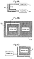
- Figures 1A-1C depict four alternative embodiments of the optically inspectable and electrically testable alignment features according to this invention.
- a first pair of alignment features is printed as part of a first conductor print
- a second pair of identical alignment features is printed as part of a successive conductor print, with no intervening dielectric.
- the alignment features depicted in Figures 1A-1C may be generally described as comprising first and second contiguous mutually perpendicular conductor segments or surfaces.
- at least one of the alignment features is in the shape of a L.
- at least one of the alignment features is in the shape of a square or rectangular box.
- the spacing between adjacent alignment features is preferably smaller than the spacing between adjacent conductors in the body of the circuit. In this way, a small degree of misalignment that does not cause shorting between adjacent conductors in the body of the circuit will be detected by shorting between the more closely spaced alignment features. Likewise, excessive conductor spread due to ink composition anomalies will be detected by shorting of the adjacent alignment features before the actual circuit features are adversely affected.
- the alignment features comprise a pair of adjacent L-shaped features 10 and 12 connected to respective probe pads 14 and 16.
- the probe pads may be printed as part of the conductor print, or may be pre-existing from an earlier print.
- one alignment feature 20 is in the shape of a box, while the other alignment feature 22 is in the shape of an adjacent box with a contiguous loop portion 22a that encircles the feature 20; in this case, probe pads are provided in the center areas of each feature.
- one alignment feature 30 is in the form of a box, and the other feature 32 is in the shape of a L having conductor segments in close proximity to two contiguous edges of the feature 30; this configuration is also shown in the testing illustration of Figure 2 and the multiple circuit illustration of Figure 3.
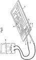
- Figure 2 illustrates off-line electrical testing of alignment using the general alignment feature topology of Figure 1C.
- various conductor patterns generally designated by the reference numeral 40 are printed on the substrate 42, and the probes 44, 46 of an electrical impedance tester 48 are placed in contact with the probe pads of the adjacent alignment features.
- the box-shaped alignment feature 30' also serves as a bond pad for the circuit, and the L-shaped alignment feature 32' is coupled to the probe pad 50.
- the tester 48 may be a digital multi-meter, or a more sophisticated piece of in-line equipment such as an automated laser trimmer/tester having probes that are automatically brought into contact with various probe and bond pads for functional testing and laser trimming.
- a particularly advantageous application of this invention may be realized with substrates that contain several independent circuits which are later separated in a singulation step.
- the above described alignment features may be printed at each circuit location on the substrate to provide an optically inspectable and electrically testable alignment check for each circuit. This can be easily achieved because the alignment features can be very small. In this way, the test equipment can be used to identify and discard circuits having improper print alignment due to localized stretching of the print screen, or localized conductor spreading, for example.
- Figure 3 illustrates a portion of a multiple circuit substrate having multiple alignment features, and a particularly advantageous embodiment in which adjacent alignment feature elements span from one circuit to another.
- the reference numeral 60 generally designates a substrate having formed thereon several identical individual circuits, identified as Circuit #1, Circuit #2, and so on. Marginal areas 62 of the substrate 60 between the various circuits are reserved to accommodate the singulation step referred to above.
- an alignment feature comprising a pair of adjacent alignment elements substantially as shown in Figure 1C is provided for each pair of adjacent circuits, although other alignment feature patterns could be used as well.
- an L-shaped alignment feature 64 electrically coupled to a bond or probe pad 66 of Circuit #1 is positioned in proximity to an existing bond or probe pad 68 at the periphery of Circuit #2.
- a similar arrangement is utilized between Circuit #'s 3 and 4, and Circuit #'s 5 and 6.
- This arrangement has two important advantages. First, it utilizes some of the marginal space 62 between adjacent circuits, instead of taking up space that would normally be used for circuit traces or elements. And second, it minimizes the impact of alignment feature shorting on any given circuit, since alignment feature shorting (due to misalignment or line spread) results only in circuit-to-circuit shorting, which will be eliminated in the singulation process anyway -- as a consequence, any existing bond or probe pad may be used as an alignment feature without having to design the circuits to tolerate inter-circuit shorting due to minor mis-alignment or line spread that causes alignment feature shorting.
- the method of this invention significantly improves the alignment testability of thick film circuits having multiple conductor print steps.
- the alignment features occupy minimal space on the circuit board, and provide both optical inspectability and electrical testability.
- Optical inspection can be carried out shortly after printing, and can be used to detect misalignment relatively early in the manufacturing process.
- Electrical testing can be carried out after firing, and is used to accurately detect misalignment sufficient to short circuit adjacent alignment features.
- the provision of multiple pairs of alignment features yields further information with minimal increase in test time since automated test equipment can test for impedance at multiple locations in parallel.
Landscapes
- Engineering & Computer Science (AREA)
- Microelectronics & Electronic Packaging (AREA)
- Manufacturing & Machinery (AREA)
- Testing Of Short-Circuits, Discontinuities, Leakage, Or Incorrect Line Connections (AREA)
- Manufacturing Of Printed Wiring (AREA)
- Structure Of Printed Boards (AREA)
Applications Claiming Priority (2)
| Application Number | Priority Date | Filing Date | Title |
|---|---|---|---|
| US94693197A | 1997-10-08 | 1997-10-08 | |
| US946931 | 1997-10-08 |
Publications (3)
| Publication Number | Publication Date |
|---|---|
| EP0909117A2 true EP0909117A2 (de) | 1999-04-14 |
| EP0909117A3 EP0909117A3 (de) | 2000-09-06 |
| EP0909117B1 EP0909117B1 (de) | 2006-01-04 |
Family
ID=25485205
Family Applications (1)
| Application Number | Title | Priority Date | Filing Date |
|---|---|---|---|
| EP19980203059 Expired - Lifetime EP0909117B1 (de) | 1997-10-08 | 1998-09-14 | Verfahren zur Herstellung von Dickfilmschaltungen |
Country Status (3)
| Country | Link |
|---|---|
| US (1) | US6143355A (de) |
| EP (1) | EP0909117B1 (de) |
| DE (1) | DE69833087T2 (de) |
Cited By (3)
| Publication number | Priority date | Publication date | Assignee | Title |
|---|---|---|---|---|
| EP1304543A1 (de) * | 2001-10-22 | 2003-04-23 | Agilent Technologies, Inc. (a Delaware corporation) | Positionieren mit leitfähigen Marken ( silicon optical bench ) |
| CN109496061A (zh) * | 2018-12-10 | 2019-03-19 | 浪潮(北京)电子信息产业有限公司 | 一种电路板的损坏判别方法和系统 |
| WO2020043580A1 (de) * | 2018-08-28 | 2020-03-05 | Siemens Aktiengesellschaft | Qualitätsmanagement für den lotpastendruck auf leiterbahnen |
Families Citing this family (5)
| Publication number | Priority date | Publication date | Assignee | Title |
|---|---|---|---|---|
| US6348742B1 (en) * | 1999-01-25 | 2002-02-19 | Clear Logic, Inc. | Sacrificial bond pads for laser configured integrated circuits |
| IT1311277B1 (it) * | 1999-12-23 | 2002-03-12 | St Microelectronics Srl | Dispositivo elettronico con collegamenti a doppio filo, metodo difabbricazione di tale dispositivo elettronico e metodo di verifica |
| US20020020491A1 (en) * | 2000-04-04 | 2002-02-21 | Price David M. | High speed flip chip assembly process |
| US6476332B1 (en) * | 2001-09-12 | 2002-11-05 | Visteon Global Technologies, Inc. | Conductor systems for thick film electronic circuits |
| US8383952B2 (en) | 2009-08-05 | 2013-02-26 | Kovio, Inc. | Printed compatible designs and layout schemes for printed electronics |
Family Cites Families (10)
| Publication number | Priority date | Publication date | Assignee | Title |
|---|---|---|---|---|
| DE2835353C2 (de) * | 1978-08-11 | 1982-05-13 | Luther & Maelzer Gmbh, 3050 Wunstorf | Verfahren zur Feststellung des Versatzes zwischen Kontaktlöchern und Leiterbahnen bei einer Leiterplatte sowie eine Leiterplatte zur Verwendung in diesem Verfahren |
| JPS58135692A (ja) * | 1982-02-06 | 1983-08-12 | 松下電器産業株式会社 | 印刷の位置決め方法 |
| FR2560437B1 (fr) * | 1984-02-28 | 1987-05-29 | Citroen Sa | Procede de report a plat d'elements de puissance sur un reseau conducteur par brasage de leurs connexions |
| US4914829A (en) * | 1988-12-16 | 1990-04-10 | Ag Communication Systems Corporation | Image alignment indicators |
| US5028867A (en) * | 1989-08-31 | 1991-07-02 | Nippon Seiki Co., Ltd. | Printed-wiring board |
| JPH03131087A (ja) * | 1989-10-17 | 1991-06-04 | Hitachi Aic Inc | プリント配線板の印刷ズレ検出方法 |
| JP2752486B2 (ja) * | 1989-12-29 | 1998-05-18 | キヤノン株式会社 | インクジェット記録ヘッドおよびその検査方法ならびにインクジェット記録装置 |
| JPH0521923A (ja) * | 1990-12-04 | 1993-01-29 | Nec Corp | 印刷配線板 |
| JPH0580104A (ja) * | 1991-09-20 | 1993-04-02 | Cmk Corp | モータ用プリント配線板の製造方法 |
| JPH05267813A (ja) * | 1992-03-24 | 1993-10-15 | Ngk Insulators Ltd | 厚膜回路基板、その製造方法および厚膜回路基板製造用基板 |
-
1998
- 1998-09-14 EP EP19980203059 patent/EP0909117B1/de not_active Expired - Lifetime
- 1998-09-14 DE DE1998633087 patent/DE69833087T2/de not_active Expired - Lifetime
-
1999
- 1999-02-16 US US09/251,248 patent/US6143355A/en not_active Expired - Fee Related
Cited By (4)
| Publication number | Priority date | Publication date | Assignee | Title |
|---|---|---|---|---|
| EP1304543A1 (de) * | 2001-10-22 | 2003-04-23 | Agilent Technologies, Inc. (a Delaware corporation) | Positionieren mit leitfähigen Marken ( silicon optical bench ) |
| US6647619B2 (en) | 2001-10-22 | 2003-11-18 | Agilent Technologies, Inc. | Positioning arrangement and method |
| WO2020043580A1 (de) * | 2018-08-28 | 2020-03-05 | Siemens Aktiengesellschaft | Qualitätsmanagement für den lotpastendruck auf leiterbahnen |
| CN109496061A (zh) * | 2018-12-10 | 2019-03-19 | 浪潮(北京)电子信息产业有限公司 | 一种电路板的损坏判别方法和系统 |
Also Published As
| Publication number | Publication date |
|---|---|
| EP0909117A3 (de) | 2000-09-06 |
| DE69833087T2 (de) | 2006-07-20 |
| EP0909117B1 (de) | 2006-01-04 |
| DE69833087D1 (de) | 2006-03-30 |
| US6143355A (en) | 2000-11-07 |
Similar Documents
| Publication | Publication Date | Title |
|---|---|---|
| US4510446A (en) | Test coupons for determining the registration of subsurface layers in a multilayer printed circuit board | |
| US10935574B2 (en) | Probe card assembly | |
| JPH02237131A (ja) | 半導体icの試験装置及び試験方法 | |
| US6249114B1 (en) | Electronic component continuity inspection method and apparatus | |
| EP0909117B1 (de) | Verfahren zur Herstellung von Dickfilmschaltungen | |
| US5263240A (en) | Method of manufacturing printed wiring boards for motors | |
| EP0926930B1 (de) | Gedruckte Schaltungsplatte | |
| US6664794B1 (en) | Apparatus and method for evaluating the surface insulation resistance of electronic assembly manufacture | |
| US20010013786A1 (en) | Apparatus and method for evaluating printed circuit board assembly manufacturing processes | |
| US4328264A (en) | Method for making apparatus for testing traces on a printed circuit board substrate | |
| JPH02198186A (ja) | プリント配線板シールド層検査方法と検査手段 | |
| US4734980A (en) | Printed circuit board wiring method | |
| KR100979502B1 (ko) | 프로브카드용 기판 | |
| JPS58172561A (ja) | プリント配線板の検査方法並びにチエツカ−治具 | |
| US6518766B2 (en) | Method of inspecting an electrical disconnection between circuits by calculating physical quantities thereof based on capacitances regarding the circuits measured twice | |
| JPS6171691A (ja) | 分割用プリント基板の分割溝配設もれ検出方法 | |
| JP3191205B2 (ja) | プリント基板の検査装置 | |
| JPH06260799A (ja) | 回路基板検査方法および回路基板 | |
| GB2215064A (en) | Testing printed circuit boards | |
| JPH05302955A (ja) | プリント配線板のパターン検査方法 | |
| JPH10190181A (ja) | プリント基板及びその検査方法 | |
| JP2000244097A (ja) | プリント配線板の導通検査方法 | |
| JPH10282177A5 (de) | ||
| JPH0621180A (ja) | プリント配線板のソルダーレジスト層の位置ずれ検査方法 | |
| JP3148116B2 (ja) | 回路基板検査装置における測定点のずれ検出方法 |
Legal Events
| Date | Code | Title | Description |
|---|---|---|---|
| PUAI | Public reference made under article 153(3) epc to a published international application that has entered the european phase |
Free format text: ORIGINAL CODE: 0009012 |
|
| AK | Designated contracting states |
Kind code of ref document: A2 Designated state(s): DE FR GB |
|
| AX | Request for extension of the european patent |
Free format text: AL;LT;LV;MK;RO;SI |
|
| RIN1 | Information on inventor provided before grant (corrected) |
Inventor name: LAUTZENHISER, FRANS PETER Inventor name: ISENBERG, JOHN KARL Inventor name: WALSH, JAMES EDWARD |
|
| PUAL | Search report despatched |
Free format text: ORIGINAL CODE: 0009013 |
|
| AK | Designated contracting states |
Kind code of ref document: A3 Designated state(s): AT BE CH CY DE DK ES FI FR GB GR IE IT LI LU MC NL PT SE |
|
| AX | Request for extension of the european patent |
Free format text: AL;LT;LV;MK;RO;SI |
|
| RAP1 | Party data changed (applicant data changed or rights of an application transferred) |
Owner name: DELPHI TECHNOLOGIES, INC. |
|
| 17P | Request for examination filed |
Effective date: 20010306 |
|
| AKX | Designation fees paid |
Free format text: DE FR GB |
|
| GRAP | Despatch of communication of intention to grant a patent |
Free format text: ORIGINAL CODE: EPIDOSNIGR1 |
|
| GRAS | Grant fee paid |
Free format text: ORIGINAL CODE: EPIDOSNIGR3 |
|
| GRAA | (expected) grant |
Free format text: ORIGINAL CODE: 0009210 |
|
| AK | Designated contracting states |
Kind code of ref document: B1 Designated state(s): DE FR GB |
|
| REG | Reference to a national code |
Ref country code: GB Ref legal event code: FG4D |
|
| REF | Corresponds to: |
Ref document number: 69833087 Country of ref document: DE Date of ref document: 20060330 Kind code of ref document: P |
|
| ET | Fr: translation filed | ||
| PLBE | No opposition filed within time limit |
Free format text: ORIGINAL CODE: 0009261 |
|
| STAA | Information on the status of an ep patent application or granted ep patent |
Free format text: STATUS: NO OPPOSITION FILED WITHIN TIME LIMIT |
|
| 26N | No opposition filed |
Effective date: 20061005 |
|
| PGFP | Annual fee paid to national office [announced via postgrant information from national office to epo] |
Ref country code: GB Payment date: 20090909 Year of fee payment: 12 |
|
| PGFP | Annual fee paid to national office [announced via postgrant information from national office to epo] |
Ref country code: DE Payment date: 20090910 Year of fee payment: 12 |
|
| PGFP | Annual fee paid to national office [announced via postgrant information from national office to epo] |
Ref country code: FR Payment date: 20091012 Year of fee payment: 12 |
|
| GBPC | Gb: european patent ceased through non-payment of renewal fee |
Effective date: 20100914 |
|
| REG | Reference to a national code |
Ref country code: FR Ref legal event code: ST Effective date: 20110531 |
|
| REG | Reference to a national code |
Ref country code: DE Ref legal event code: R119 Ref document number: 69833087 Country of ref document: DE Effective date: 20110401 |
|
| PG25 | Lapsed in a contracting state [announced via postgrant information from national office to epo] |
Ref country code: FR Free format text: LAPSE BECAUSE OF NON-PAYMENT OF DUE FEES Effective date: 20100930 Ref country code: DE Free format text: LAPSE BECAUSE OF NON-PAYMENT OF DUE FEES Effective date: 20110401 |
|
| PG25 | Lapsed in a contracting state [announced via postgrant information from national office to epo] |
Ref country code: GB Free format text: LAPSE BECAUSE OF NON-PAYMENT OF DUE FEES Effective date: 20100914 |