EP0921555A2 - Procédé de lithographie par faisceau d'électrons utilisant des marques d'alignement positionnées de manière univoque et tranche comportant de telles marques d'alignement - Google Patents
Procédé de lithographie par faisceau d'électrons utilisant des marques d'alignement positionnées de manière univoque et tranche comportant de telles marques d'alignement Download PDFInfo
- Publication number
- EP0921555A2 EP0921555A2 EP98123008A EP98123008A EP0921555A2 EP 0921555 A2 EP0921555 A2 EP 0921555A2 EP 98123008 A EP98123008 A EP 98123008A EP 98123008 A EP98123008 A EP 98123008A EP 0921555 A2 EP0921555 A2 EP 0921555A2
- Authority
- EP
- European Patent Office
- Prior art keywords
- wafer
- alignment marks
- chip regions
- center point
- alignment
- Prior art date
- Legal status (The legal status is an assumption and is not a legal conclusion. Google has not performed a legal analysis and makes no representation as to the accuracy of the status listed.)
- Withdrawn
Links
Images


Classifications
-
- G—PHYSICS
- G03—PHOTOGRAPHY; CINEMATOGRAPHY; ANALOGOUS TECHNIQUES USING WAVES OTHER THAN OPTICAL WAVES; ELECTROGRAPHY; HOLOGRAPHY
- G03F—PHOTOMECHANICAL PRODUCTION OF TEXTURED OR PATTERNED SURFACES, e.g. FOR PRINTING, FOR PROCESSING OF SEMICONDUCTOR DEVICES; MATERIALS THEREFOR; ORIGINALS THEREFOR; APPARATUS SPECIALLY ADAPTED THEREFOR
- G03F9/00—Registration or positioning of originals, masks, frames, photographic sheets or textured or patterned surfaces, e.g. automatically
- G03F9/70—Registration or positioning of originals, masks, frames, photographic sheets or textured or patterned surfaces, e.g. automatically for microlithography
- G03F9/7073—Alignment marks and their environment
- G03F9/7076—Mark details, e.g. phase grating mark, temporary mark
-
- H—ELECTRICITY
- H10—SEMICONDUCTOR DEVICES; ELECTRIC SOLID-STATE DEVICES NOT OTHERWISE PROVIDED FOR
- H10W—GENERIC PACKAGES, INTERCONNECTIONS, CONNECTORS OR OTHER CONSTRUCTIONAL DETAILS OF DEVICES COVERED BY CLASS H10
- H10W46/00—Marks applied to devices, e.g. for alignment or identification
-
- H—ELECTRICITY
- H01—ELECTRIC ELEMENTS
- H01J—ELECTRIC DISCHARGE TUBES OR DISCHARGE LAMPS
- H01J37/00—Discharge tubes with provision for introducing objects or material to be exposed to the discharge, e.g. for the purpose of examination or processing thereof
- H01J37/30—Electron-beam or ion-beam tubes for localised treatment of objects
- H01J37/304—Controlling tubes by information coming from the objects or from the beam, e.g. correction signals
- H01J37/3045—Object or beam position registration
-
- H—ELECTRICITY
- H10—SEMICONDUCTOR DEVICES; ELECTRIC SOLID-STATE DEVICES NOT OTHERWISE PROVIDED FOR
- H10W—GENERIC PACKAGES, INTERCONNECTIONS, CONNECTORS OR OTHER CONSTRUCTIONAL DETAILS OF DEVICES COVERED BY CLASS H10
- H10W46/00—Marks applied to devices, e.g. for alignment or identification
- H10W46/101—Marks applied to devices, e.g. for alignment or identification characterised by the type of information, e.g. logos or symbols
-
- H—ELECTRICITY
- H10—SEMICONDUCTOR DEVICES; ELECTRIC SOLID-STATE DEVICES NOT OTHERWISE PROVIDED FOR
- H10W—GENERIC PACKAGES, INTERCONNECTIONS, CONNECTORS OR OTHER CONSTRUCTIONAL DETAILS OF DEVICES COVERED BY CLASS H10
- H10W46/00—Marks applied to devices, e.g. for alignment or identification
- H10W46/301—Marks applied to devices, e.g. for alignment or identification for alignment
-
- H—ELECTRICITY
- H10—SEMICONDUCTOR DEVICES; ELECTRIC SOLID-STATE DEVICES NOT OTHERWISE PROVIDED FOR
- H10W—GENERIC PACKAGES, INTERCONNECTIONS, CONNECTORS OR OTHER CONSTRUCTIONAL DETAILS OF DEVICES COVERED BY CLASS H10
- H10W46/00—Marks applied to devices, e.g. for alignment or identification
- H10W46/501—Marks applied to devices, e.g. for alignment or identification for use before dicing
- H10W46/503—Located in scribe lines
-
- H—ELECTRICITY
- H10—SEMICONDUCTOR DEVICES; ELECTRIC SOLID-STATE DEVICES NOT OTHERWISE PROVIDED FOR
- H10W—GENERIC PACKAGES, INTERCONNECTIONS, CONNECTORS OR OTHER CONSTRUCTIONAL DETAILS OF DEVICES COVERED BY CLASS H10
- H10W46/00—Marks applied to devices, e.g. for alignment or identification
- H10W46/601—Marks applied to devices, e.g. for alignment or identification for use after dicing
- H10W46/603—Formed on wafers or substrates before dicing and remaining on chips after dicing
-
- Y—GENERAL TAGGING OF NEW TECHNOLOGICAL DEVELOPMENTS; GENERAL TAGGING OF CROSS-SECTIONAL TECHNOLOGIES SPANNING OVER SEVERAL SECTIONS OF THE IPC; TECHNICAL SUBJECTS COVERED BY FORMER USPC CROSS-REFERENCE ART COLLECTIONS [XRACs] AND DIGESTS
- Y10—TECHNICAL SUBJECTS COVERED BY FORMER USPC
- Y10S—TECHNICAL SUBJECTS COVERED BY FORMER USPC CROSS-REFERENCE ART COLLECTIONS [XRACs] AND DIGESTS
- Y10S438/00—Semiconductor device manufacturing: process
- Y10S438/975—Substrate or mask aligning feature
Definitions
- the present invention relates generally to improvements in electron beam exposure for writing desired patterns on a semiconductor water, and more specifically to a method of implementing electron beam lithography using uniquely positioned alignment marks. Still more specifically, the present invention relates to a semiconductor wafer itself which is previously provided with the above mentioned alignment marks.
- Electron beam lithography (viz., electron beam exposure) has the advantage of being able to eliminate the need for reticles or masks each representing a circuit pattern to be formed. As is known, the electron beam exposure is able to directly write or draw patterns in accordance with circuit design data outputted from a CAD (computer aided design) system.
- CAD computer aided design
- electron beam lithography is typically used to produce semiconductor devices, such as ASICs (application specific integrated circuits), custom ICs (integrated circuit), etc., each of which is of multi-sort but small-production quantities and which is required to be delivered within a limited time.
- ASICs application specific integrated circuits
- custom ICs integrated circuit
- the sequence of IC fabrication consists of multiple processing steps that add, alter and remove thin layers. Each of these processing steps requires extremely strict alignment or registration. To this end, alignment marks are formed on a semiconductor water and are used as references for aligning at each processing step.
- an alignment mark which is to be used in a subsequent step, is formed in each chip region during the first exposing process via which cell segregation layers are formed. That is, the cell segregation layers can be formed in the range of alignment precision of a stepper itself. Accordingly, in the case of photolithography, there is no need to provide a processing step dedicated to forming the alignment marks.
- the alignment is implemented by detecting electron beams reflected at an alignment mark.
- the alignment mark is formed so as to have a height sufficient to enable the detection of the mark in the manner disclosed. Therefore, in the case of electron beam lithography, it is necessary to provide a processing stage which is dedicated to forming alignment marks prior to the first actual IC fabrication process of forming cell separation layers.
- a silicon semiconductor wafer 10 is provided with a plurality of alignment marks 12. These marks are respectively formed within corresponding chip regions 14 each of which is square or rectangular and indicated by a broken line. Each alignment mark is cross-shaped in this particular case.
- chip region implies a region on which electronic circuitry is to be formed. After all the processing steps on the wafer have been completed, the wafer is cut into a plurality of chips (viz., diced) and packaged. The area or region between adjacent chip regions 14 is a dicing region or margin.
- the chip regions 14 respectively carry the cross-shaped alignment marks 12 in the same positions thereof, each of which has been determined considering the size of the chip to be fabricated and the arrangement of the chip regions 14.
- a reticle is prepared taking the chip size into account.
- the mark 12 is formed via photolithographic techniques using step-repeat optical exposure of a stepper.
- the linear strip-like spaces, which are formed between the adjacent chip regions 14, are dicing regions or scribe dines along which the wafer is cut into individual chips.
- An EGA (enhanced global alignment) method disclosed in the Japanese Patent Application Tokkai-hei No. 8-181066 is classified as one kind of the global alignment. In order to implement the electron beam exposure using the global alignment, it is necessary to detect a plurality of alignment marks 12.
- the aforesaid conventional technique has encountered the problem that the chip size can not be determined until the circuit design is completely finished, which results in a long turnaround time.
- the conventional technique suffers from the difficulty that the turnaround time become extremely long.
- Another object of the present invention is to provide a wafer with alignment marks formed in a region which is not affected by chip size and chip region arrangement.
- these objects are achieved by an arrangement wherein a plurality of alignment marks are formed on a semiconductor wafer in an area outside a plurality of chip regions, such as in a periphery of the wafer, irrespectively of the size and arrangement of the chip regions.
- Such wafers which are previously manufactured, are then subjected to electron beam exposure in accordance with circuit design data.
- the electron beam exposure is typically implemented through global alignment using the alignment marks.
- One aspect of the present invention resides in a method of forming electronic circuitry on a semiconductor wafer using electron beam lithography, comprising the steps of: (a) forming, on the wafer, a plurality of alignment marks in an area on which a plurality of chip regions in which the electronic circuitry is to be formed, are absent; and (b) implementing a series of processing steps for forming the electronic circuitry in the chip regions using the alignment marks for alignment.
- Another aspect of the present invention resides in a semiconductor wafer on which electronic circuitry is to be formed in each of a plurality of scheduled chip regions using electronic beam lithography, characterized in that the wafer carries a plurality of alignment marks formed in an area which is separated or distinct from that in which the plurality of scheduled chip regions are formed.
- the alignment marks are formed in the region, such as about the periphery of a wafer, which are not included in any chip region.
- the positions, at which the alignment marks are formed are in the region in which the chips are not formed but which is, however, preferably subjected to the subsequent fabrication steps such as layer deposition or etching.
- Such positions are defined about a wafer's peripheral area but re separated from the wafer's edge by slightly more than 5 mm (for example), and/or are located in an area which becomes a dicing area irrespectively of chip sizes.
- a semiconductor wafer may be round if the wafer is not provided with an orientation flat, and has a center point in the vicinity of the supposed round's center point. Since a plurality of chips are cut from a semiconductor wafer using a dicing saw, each dicing region (viz., scribe line) is a striplike region which crosses the semiconductor wafer. Therefore, the chip regions are provided in a manner that a group consisting of 2 ⁇ 2 chip regions is symmetrically repeated in two-dimensional directions on the wafer. The center point of the wafer therefore becomes the symmetrical center point of the chip regions arranged in lattice. The center point accordingly is included in the dicing region irrespective of the chip size and thus, an alignment mark can be provided at this center point.
- center point of a wafer is typically included in a crossed area of two dicing regions in parallel with and normal to the orientation flat and accordingly, an alignment mark may be provided thereat.
- An alignment mark which is made of a semiconductor material, is a step formed on the wafer.
- an alignment mark is made of metal, such as a heavy metal, which is formed on the wafer and which is able to reflect a large amount of electrons when bombarded by an electron beam.
- the number of alignment marks to be provided will be considered below. Three alignment marks, which are not provided on a straight line, mathematically define one plane, and thus are used to implement minimum global alignment. However, in order to achieve high alignment accuracy, it is important to provide four and more alignment marks. In this case, as the area of a polygon defined by a plurality of alignment marks becomes large, the alignment accuracy increases and therefore, it is preferable to provide six or more alignment marks around the periphery of the wafer. Further, in order to compensate for local distortion, it is preferable to provide an alignment mark at the center portion of the semiconductor wafer.
- each alignment mark should be used only once for the alignment purpose (viz., should be a disposable). Therefore, a plurality of alignment mark groups are prepared, and each of the groups consists of the alignment marks whose number meets the number of processes each requiring one alignment mark.
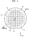
- a semiconductor wafer 20 is made of silicon and is provided with substantially rectangular chip regions 22 whose number is preferably an even multiple of four (merely for example). As shown In Fig. 2, a plurality of the chip regions 22, amounting to fifty-two (52) in total and having sizes or shapes identical with each other, are arranged in a lattice. That is, the chip regions 22 are arranged, from top to bottom, in a manner of one row including 4 chip regions, one row including 6 chip regions, four rows each including 8 chip regions, one row including 6 chip regions, and one row including 4 chip regions. Accordingly, the center point surrounded by four center chip regions coincides with a center point O of the wafer 20 and is located in a dicing region. It is understood that if all the chip regions 22 are symmetrically formed, the center point of symmetrical arranged chip regions 22 is coincidental with the wafers center point O irrespective of the chip sizes.
- a cross-shaped alignment mark 24 is provided at the wafer's center point O. Further, other eleven cross-shaped alignment marks 24 are substantially equally spaced about the periphery of the semiconductor wafer 20 in a manner where each of the marks is located at a predetermined distance (5 mm for example) from the wafer's edge.
- the center point O of the wafer 20 is uniquely defined, the center point O coincides with the center point of the chip arrangement and is located in the dicing region.
- the chip regions 22 are each equally shaped and are arranged in the lattice, the above mentioned relationship coincidence is not affected irrespective of the facts that the size of each chip region is uniformly changed, and the number of the chip regions 22 varies. Accordingly, the alignment mark 24 at the water's center point O is always located outside the chip regions 22 irrespective of the fact of the chip size and the number of the chip regions 22.
- the periphery of the semiconductor wafer 20 is the area used for holding and transporting the wafer 20 between fabrication processes, and is not typically subjected to any fabrication process such as layer deposition.
- a peripheral region has a width of approximately 5mm from the water's edge (by way of example).
- each of the alignment marks 24, provided at the periphery of the semiconductor wafer 11, is located in a region which is slightly inside the peripheral region provided for wafer holding and transportation and which is therefore uniformly subjected to layer deposition and etching. It is understood that each of the peripheral positions at which the marks 24 are formed is outside the chip regions 22 irrespective of the chip size.
- Each alignment mark 24 may be formed using photolithography or electron beam lithography.
- the alignment mark 24 is formed using a so-called shot map function of a stepper after preparing a reticle having only a pattern representing the alignment mark 24. It is understood that the above mentioned reticle has no relationship with the kinds of ASICs and custom ICs to be manufactured. Further, it is sufficient to prepare only one reticle which can commonly be used for forming the alignment mark 24.
- Each alignment mark 24 is made of a semiconductor material such as silicon and is formed so as to have a step height of about more than 0.3 ⁇ m (for example).
- the alignment mark 24 can be formed using a suitable heavy metal, in the case of which the step height may be less than 0.3 ⁇ m (for example).
- the alignment mark 24 is preferably shaped such as to have one or more edge sides parallel with each of X- and Y-axes of the semiconductor wafer 11. The length of the side has a range approximately between 30 and 50 ⁇ m (for example).
- Figs. 3(A)-3(D) show examples of possible shapes of the alignment mark 24.
- each of the hatched portions indicates a portion that is higher or lower than the surrounding portion thereof.
- the region defined between a rectangle 30 depicted by a solid line and the hatchet portion is lowered or etched using a positive resist.
- the hatched portion has the same level as the other region of the wafer 20 at the stage of forming the alignment marks 24.
- each alignment mark 24 is formed in a region separate from that for the chip regions 22 irrespective of the chip size and the number of chips formed on the wafer. Therefore, at the stage of forming the alignment marks 24, there is no need to have determined the chip size and the arrangement of the chip regions 22. Thereafter, with the aid of a CAD system, the circuit pattern, the chip size, and the arrangement of the chip regions 22 on the wafer 11, are determined. When the designed chip regions 22 on the wafer 20 have been completed, the electron beam patterning is implemented on the wafer 20, at the time of which the exposure alignment is implemented. In the instant embodiment, it is assumed that each alignment mark 24 is used, by way of global alignment, to compensate for shift, gain, rotation, etc.
- Fig. 4 is a drawing schematically showing a principle of detecting the alignment mark 24 during electron beam exposure.
- An electron beam 42 emitted from an electron gun 44 is deflected and scanned by a deflector 46 over the water. 20.
- Reflected or backscattered electrons which occur when the electron beam 42 bombards the surface of the wafer 20, are detected by a reflected electron detector 48 comprising a plurality of multi-channel plates.
- the reflected electrons thus detected are amplified at an amplifier 50 and fed to an edge detector 52. While scanning the wafer 20 using the electron beam 42, the edges of the alignment mark 24 are detected by the edge detector 52 whereby the position of the alignment mark 24 on the wafer 20 can be ascertained.
- FIG. 5(A) shows a relationship between the electron beam scanning and the resulting electrical signal in the case where the alignment mark 24 is a step made of silicon.
- Fig. 5(B) illustrates a relationship between the electron beam scanning and the obtained electrical signal when the alignment mark 24 is made of a heavy metal.
- the alignment marks 24 are formed in the area outside the chip regions 24 irrespective of the chip size. Therefore, before determining the circuit pattern in each chip region and the overall arrangement of chip regions on the wafer, it is possible to implement the step of forming the alignment marks. This is very advantageous because it is possible to use a single type of wafers each of which carries the above mentioned alignment marks 24.
- each of the alignment marks 24 is exemplary and that the invention is in no way limited thereto.
- FIG. 6 wherein a second embodiment of the present invention is illustrated.
- no alignment mark is formed at the center point O of the wafer 20.
- a plurality of alignment marks 24 are grouped and formed only about the periphery of the wafer 20. That is, eight groups 62(a)-62(h), each of which comprises four alignment marks 24, are provided at substantially equal intervals.
- the reason why the multiple alignment marks 24 are grouped is that a mark is not used twice. Therefore, the number of the alignment marks 24 in each group corresponds to the number of IC fabrication processes wherein the mark is indispensable for alignment.
- the gate electrodes or metal connection lines are formed, these layer elements are able to be utilized for alignment and hence, it is sufficient if each group includes the alignment marks the number of which equals the number of fabrication processes until forming the electrodes, etc.
- the water 20 according to the third embodiment is further provided with additional eight alignment marks 24 compared to the first embodiment of Fig. 1. Since the chip regions 22 are symmetrically provided with respect to orthogonal (vertical and horizontal) lines passing through the center point O, the additional alignment marks 24 can be formed on the two strip-like dicing regions which intersect at the water's center point O. By thus providing the alignment marks 24, the alignment can be made precisely without being affected by local distortion of the wafer 20.
Landscapes
- Chemical & Material Sciences (AREA)
- Analytical Chemistry (AREA)
- Physics & Mathematics (AREA)
- General Physics & Mathematics (AREA)
- Electron Beam Exposure (AREA)
- Exposure And Positioning Against Photoresist Photosensitive Materials (AREA)
- Exposure Of Semiconductors, Excluding Electron Or Ion Beam Exposure (AREA)
Applications Claiming Priority (2)
| Application Number | Priority Date | Filing Date | Title |
|---|---|---|---|
| JP33458897A JP3169068B2 (ja) | 1997-12-04 | 1997-12-04 | 電子線露光方法及び半導体ウエハ |
| JP33458897 | 1997-12-04 |
Publications (2)
| Publication Number | Publication Date |
|---|---|
| EP0921555A2 true EP0921555A2 (fr) | 1999-06-09 |
| EP0921555A3 EP0921555A3 (fr) | 2001-10-24 |
Family
ID=18279086
Family Applications (1)
| Application Number | Title | Priority Date | Filing Date |
|---|---|---|---|
| EP98123008A Withdrawn EP0921555A3 (fr) | 1997-12-04 | 1998-12-04 | Procédé de lithographie par faisceau d'électrons utilisant des marques d'alignement positionnées de manière univoque et tranche comportant de telles marques d'alignement |
Country Status (6)
| Country | Link |
|---|---|
| US (1) | US6132910A (fr) |
| EP (1) | EP0921555A3 (fr) |
| JP (1) | JP3169068B2 (fr) |
| KR (1) | KR100310497B1 (fr) |
| CN (1) | CN1221209A (fr) |
| TW (1) | TW464939B (fr) |
Cited By (5)
| Publication number | Priority date | Publication date | Assignee | Title |
|---|---|---|---|---|
| WO2000079566A1 (fr) * | 1999-06-22 | 2000-12-28 | Etec Systems, Inc. | Alignement de faisceaux d'electrons de faible energie a l'aide de champs magnetiques |
| WO2002031868A1 (fr) * | 2000-10-10 | 2002-04-18 | Toray Engineering Co., Ltd. | Procede d'alignement de plaquettes empilees |
| WO2009007930A3 (fr) * | 2007-07-12 | 2009-04-30 | Nxp Bv | Circuits intégrés sur une tranche et procédé de séparation des circuits intégrés sur une tranche |
| WO2010013194A3 (fr) * | 2008-07-26 | 2010-10-14 | X-Fab Semiconductor Foundries Ag | Orientation d'une structure électronique cmos relativement à une structure enfouie dans des empilements de tranches semiconductrices présentant des connexions et des amincissements |
| US9466324B2 (en) | 2013-10-31 | 2016-10-11 | Seagate Technology Llc | Bit patterned media template including alignment mark and method of using same |
Families Citing this family (42)
| Publication number | Priority date | Publication date | Assignee | Title |
|---|---|---|---|---|
| US6235141B1 (en) | 1996-09-27 | 2001-05-22 | Digital Optics Corporation | Method of mass producing and packaging integrated optical subsystems |
| JP4454706B2 (ja) * | 1998-07-28 | 2010-04-21 | キヤノン株式会社 | 電子ビーム露光方法及び装置、ならびにデバイス製造方法 |
| US6479887B1 (en) * | 1998-08-31 | 2002-11-12 | Amkor Technology, Inc. | Circuit pattern tape for wafer-scale production of chip size semiconductor packages |
| US6428641B1 (en) | 1998-08-31 | 2002-08-06 | Amkor Technology, Inc. | Method for laminating circuit pattern tape on semiconductor wafer |
| US6781680B1 (en) * | 1999-03-26 | 2004-08-24 | Kabushiki Kaisha Toshiba | Optical system adjusting method for energy beam apparatus |
| WO2001009927A1 (fr) * | 1999-07-28 | 2001-02-08 | Infineon Technologies North America Corp. | Structures a semi-conducteurs et leurs procedes de fabrication |
| US6576529B1 (en) * | 1999-12-07 | 2003-06-10 | Agere Systems Inc. | Method of forming an alignment feature in or on a multilayered semiconductor structure |
| US6383894B1 (en) * | 2000-03-31 | 2002-05-07 | Intel Corporation | Method of forming scribe line planarization layer |
| US6943429B1 (en) * | 2001-03-08 | 2005-09-13 | Amkor Technology, Inc. | Wafer having alignment marks extending from a first to a second surface of the wafer |
| US6869861B1 (en) | 2001-03-08 | 2005-03-22 | Amkor Technology, Inc. | Back-side wafer singulation method |
| JP4071476B2 (ja) * | 2001-03-21 | 2008-04-02 | 株式会社東芝 | 半導体ウェーハ及び半導体ウェーハの製造方法 |
| CN100438015C (zh) * | 2001-03-21 | 2008-11-26 | 株式会社东芝 | 具有id标记的半导体晶片,及从中生产半导体器件的方法和设备 |
| WO2003003798A1 (fr) * | 2001-06-29 | 2003-01-09 | Toray Engineering Co., Ltd. | Methode d'assemblage utilisant un adhesif conducteur anisotrope |
| US6953956B2 (en) * | 2002-12-18 | 2005-10-11 | Easic Corporation | Semiconductor device having borderless logic array and flexible I/O |
| SG121844A1 (en) * | 2002-12-20 | 2006-05-26 | Asml Netherlands Bv | Device manufacturing method |
| KR100519948B1 (ko) * | 2003-05-20 | 2005-10-10 | 엘지.필립스 엘시디 주식회사 | 비정질 실리콘의 결정화 공정 및 이를 이용한 스위칭 소자 |
| JP4809600B2 (ja) * | 2003-10-28 | 2011-11-09 | 株式会社半導体エネルギー研究所 | 半導体装置の作製方法 |
| KR100578916B1 (ko) * | 2003-12-19 | 2006-05-11 | 삼성에스디아이 주식회사 | 옵셋공정의 얼라인 마크 형성방법 및 그 장치 |
| US7453160B2 (en) * | 2004-04-23 | 2008-11-18 | Axcelis Technologies, Inc. | Simplified wafer alignment |
| JP4253707B2 (ja) * | 2004-04-28 | 2009-04-15 | 株式会社ブイ・テクノロジー | 露光パターン形成方法 |
| US7259828B2 (en) * | 2004-05-14 | 2007-08-21 | Asml Netherlands B.V. | Alignment system and method and device manufactured thereby |
| JP4731886B2 (ja) * | 2004-11-12 | 2011-07-27 | 株式会社ブイ・テクノロジー | 液晶表示装置用基板の製造方法 |
| US7459247B2 (en) * | 2004-12-27 | 2008-12-02 | Asml Netherlands B.V. | Lithographic apparatus and device manufacturing method |
| KR100666465B1 (ko) * | 2004-12-28 | 2007-01-11 | 동부일렉트로닉스 주식회사 | 웨이퍼에 대한 정렬용 마크 표시 방법 |
| JP4837971B2 (ja) * | 2005-10-07 | 2011-12-14 | ルネサスエレクトロニクス株式会社 | 半導体装置の製造方法 |
| JP5139658B2 (ja) * | 2006-09-21 | 2013-02-06 | 株式会社ニューフレアテクノロジー | 描画データ処理制御装置 |
| US20080265445A1 (en) * | 2007-04-30 | 2008-10-30 | International Business Machines Corporation | Marks for the Alignment of Wafer-Level Underfilled Silicon Chips and Method to Produce Same |
| JP2009216844A (ja) * | 2008-03-10 | 2009-09-24 | Seiko Instruments Inc | 縮小投影露光装置用レチクルおよびそれを用いた露光方法 |
| CN102683238B (zh) * | 2012-05-04 | 2015-07-22 | 上海华力微电子有限公司 | 一种提高图形线宽量测精度对准的方法 |
| JP6084143B2 (ja) * | 2013-09-30 | 2017-02-22 | ソニーセミコンダクタソリューションズ株式会社 | 半導体デバイスおよび製造方法、並びに電子機器 |
| US9601436B2 (en) * | 2014-06-06 | 2017-03-21 | Taiwan Semiconductor Manufacturing Co., Ltd | Method for semiconductor wafer alignment |
| JP6357064B2 (ja) * | 2014-09-30 | 2018-07-11 | 株式会社Screenホールディングス | パターン形成装置およびパターン形成方法 |
| CN104635432B (zh) * | 2015-01-27 | 2017-04-12 | 中国科学院物理研究所 | 用于电子束曝光的待曝光衬底及对准标记定位的方法 |
| US9659873B2 (en) | 2015-08-26 | 2017-05-23 | United Microelectronics Corp. | Semiconductor structure with aligning mark and method of forming the same |
| CN106004096B (zh) * | 2016-05-13 | 2018-05-04 | 清华大学深圳研究生院 | 一种用于打印石英晶体传感器敏感层的喷墨打印托盘 |
| CN109307981B (zh) * | 2017-07-26 | 2022-03-22 | 天津环鑫科技发展有限公司 | 一种gpp生产的光刻版工艺 |
| CN109240038A (zh) * | 2018-10-15 | 2019-01-18 | 上海华虹宏力半导体制造有限公司 | 一种掩模板、晶圆及其曝光方法、封装方法 |
| CN109375472A (zh) * | 2018-10-23 | 2019-02-22 | 武汉华星光电技术有限公司 | 曝边机及基板曝边方法 |
| CN115176415A (zh) * | 2020-04-09 | 2022-10-11 | 株式会社村田制作所 | 集合基板的制造方法以及集合基板 |
| CN115132719B (zh) * | 2021-03-26 | 2025-01-28 | 世芯电子股份有限公司 | 集成电路产品及其芯片排布 |
| JP2022176696A (ja) * | 2021-05-17 | 2022-11-30 | 富士電機株式会社 | 炭化珪素半導体装置の製造方法 |
| CN114171500B (zh) * | 2021-12-07 | 2024-04-09 | 成都海威华芯科技有限公司 | 一种版图定位标记绘制方法、基于其制备的芯片及晶圆 |
Family Cites Families (14)
| Publication number | Priority date | Publication date | Assignee | Title |
|---|---|---|---|---|
| US4407933A (en) * | 1981-06-11 | 1983-10-04 | Bell Telephone Laboratories, Incorporated | Alignment marks for electron beam lithography |
| JPS5946026A (ja) * | 1982-09-09 | 1984-03-15 | Toshiba Corp | 試料位置測定方法 |
| JPH01204419A (ja) * | 1988-02-09 | 1989-08-17 | Nec Corp | 荷電ビーム露光装置 |
| JPH0582428A (ja) * | 1991-09-20 | 1993-04-02 | Hitachi Ltd | 電子線描画装置 |
| JP3335011B2 (ja) * | 1994-09-16 | 2002-10-15 | 富士通株式会社 | マスク及びこれを用いる荷電粒子ビーム露光方法 |
| JP3258178B2 (ja) * | 1994-09-27 | 2002-02-18 | 株式会社東芝 | 位置合わせ方法 |
| US5552611A (en) * | 1995-06-06 | 1996-09-03 | International Business Machines | Pseudo-random registration masks for projection lithography tool |
| JPH09148217A (ja) * | 1995-11-17 | 1997-06-06 | Mitsubishi Electric Corp | 位置合わせ方法 |
| JP2870461B2 (ja) * | 1995-12-18 | 1999-03-17 | 日本電気株式会社 | フォトマスクの目合わせマーク及び半導体装置 |
| KR100467858B1 (ko) * | 1996-02-05 | 2005-11-01 | 가부시키가이샤 니콘 | 정렬,노광방법및노광장치 |
| US6159644A (en) * | 1996-03-06 | 2000-12-12 | Hitachi, Ltd. | Method of fabricating semiconductor circuit devices utilizing multiple exposures |
| JPH09275058A (ja) * | 1996-04-04 | 1997-10-21 | Nikon Corp | 投影露光方法 |
| US5837404A (en) * | 1997-01-04 | 1998-11-17 | Holtek Microelectronics, Inc. | Fabrication of zero layer mask |
| JPH10274855A (ja) * | 1997-03-31 | 1998-10-13 | Mitsubishi Electric Corp | レチクルおよびそれによって転写されたパターンならびに補正方法 |
-
1997
- 1997-12-04 JP JP33458897A patent/JP3169068B2/ja not_active Expired - Fee Related
-
1998
- 1998-12-03 KR KR1019980052903A patent/KR100310497B1/ko not_active Expired - Fee Related
- 1998-12-03 US US09/204,940 patent/US6132910A/en not_active Expired - Fee Related
- 1998-12-04 CN CN98126725A patent/CN1221209A/zh active Pending
- 1998-12-04 TW TW087120236A patent/TW464939B/zh not_active IP Right Cessation
- 1998-12-04 EP EP98123008A patent/EP0921555A3/fr not_active Withdrawn
Cited By (9)
| Publication number | Priority date | Publication date | Assignee | Title |
|---|---|---|---|---|
| WO2000079566A1 (fr) * | 1999-06-22 | 2000-12-28 | Etec Systems, Inc. | Alignement de faisceaux d'electrons de faible energie a l'aide de champs magnetiques |
| WO2002031868A1 (fr) * | 2000-10-10 | 2002-04-18 | Toray Engineering Co., Ltd. | Procede d'alignement de plaquettes empilees |
| KR100771362B1 (ko) * | 2000-10-10 | 2007-10-30 | 토레이 엔지니어링 컴퍼니, 리미티드 | 적층 웨이퍼의 얼라인먼트 방법 |
| WO2009007930A3 (fr) * | 2007-07-12 | 2009-04-30 | Nxp Bv | Circuits intégrés sur une tranche et procédé de séparation des circuits intégrés sur une tranche |
| US8415769B2 (en) | 2007-07-12 | 2013-04-09 | Nxp B.V. | Integrated circuits on a wafer and method for separating integrated circuits on a wafer |
| WO2010013194A3 (fr) * | 2008-07-26 | 2010-10-14 | X-Fab Semiconductor Foundries Ag | Orientation d'une structure électronique cmos relativement à une structure enfouie dans des empilements de tranches semiconductrices présentant des connexions et des amincissements |
| US8691658B2 (en) | 2008-07-26 | 2014-04-08 | X-Fab Semiconductor Foundries Ag | Orientation of an electronic CMOS structure with respect to a buried structure in the case of a bonded and thinned-back stack of semiconductor wafers |
| US9466324B2 (en) | 2013-10-31 | 2016-10-11 | Seagate Technology Llc | Bit patterned media template including alignment mark and method of using same |
| US9964855B2 (en) | 2013-10-31 | 2018-05-08 | Seagate Technology Llc | Bit patterned media template including alignment mark and method of using same |
Also Published As
| Publication number | Publication date |
|---|---|
| JP3169068B2 (ja) | 2001-05-21 |
| KR19990062773A (ko) | 1999-07-26 |
| EP0921555A3 (fr) | 2001-10-24 |
| KR100310497B1 (ko) | 2001-11-15 |
| US6132910A (en) | 2000-10-17 |
| JPH11168053A (ja) | 1999-06-22 |
| TW464939B (en) | 2001-11-21 |
| CN1221209A (zh) | 1999-06-30 |
Similar Documents
| Publication | Publication Date | Title |
|---|---|---|
| US6132910A (en) | Method of implementing electron beam lithography using uniquely positioned alignment marks and a wafer with such alignment marks | |
| US5777392A (en) | Semiconductor device having improved alignment marks | |
| US5017514A (en) | Method of manufacturing a semiconductor device using a main vernier pattern formed at a right angle to a subsidiary vernier pattern | |
| US7126231B2 (en) | Mask-making member and its production method, mask and its making method, exposure process, and fabrication method of semiconductor device | |
| US5982044A (en) | Alignment pattern and algorithm for photolithographic alignment marks on semiconductor substrates | |
| US20030235330A1 (en) | Position detection apparatus, position detection method, exposure apparatus, device manufacturing method, and substrate | |
| EP0130819B1 (fr) | Procédé pour le positionnement d'un faisceau à une partie spécifique d'une pastille semi-conductrice | |
| US20060278956A1 (en) | Semiconductor wafer with non-rectangular shaped dice | |
| US5552611A (en) | Pseudo-random registration masks for projection lithography tool | |
| EP0078579B1 (fr) | Méthode d'utilisation d'un faisceau d'électrons | |
| EP0033138B1 (fr) | Procédé pour corriger les distorsions de déviation dans un appareil pour lithographie à particules chargées | |
| EP0022329B1 (fr) | Procédé d'exposition à un faisceau d'electrons | |
| EP0078578B1 (fr) | Méthode d'utilisation d'un faisceau d'électrons | |
| EP1548806A1 (fr) | Procede d'alignement, substrat d'alignement, procede de production d'un substrat d'alignement, procede d'exposition, systeme d'exposition et procede de production d'un masque | |
| JPH04252016A (ja) | パターン描画方法 | |
| JP2003515918A (ja) | レチクルとウェハとの間のミスアラインメントを判定するための方法 | |
| JPS62159441A (ja) | 位置合せマ−ク | |
| US6784974B1 (en) | Exposure method and exposure apparatus | |
| KR100214266B1 (ko) | 이빔 리소그라피에 적용되는 셀 어퍼처 | |
| JPH10185541A (ja) | 配置精度測定方法、フォトマスク及び半導体装置 | |
| JPH0325010B2 (fr) | ||
| JPS6269518A (ja) | 電子ビ−ム露光方法 | |
| JPS6142409B2 (fr) | ||
| JPH1140481A (ja) | 電子線露光用マスク及びこれを用いた電子線露光装置 | |
| JPH11145037A (ja) | 電子ビーム描画装置及びマーク位置の検出方法 |
Legal Events
| Date | Code | Title | Description |
|---|---|---|---|
| PUAI | Public reference made under article 153(3) epc to a published international application that has entered the european phase |
Free format text: ORIGINAL CODE: 0009012 |
|
| AK | Designated contracting states |
Kind code of ref document: A2 Designated state(s): AT BE CH CY DE DK ES FI FR GB GR IE IT LI LU MC NL PT SE Kind code of ref document: A2 Designated state(s): DE GB |
|
| AX | Request for extension of the european patent |
Free format text: AL;LT;LV;MK;RO;SI |
|
| PUAL | Search report despatched |
Free format text: ORIGINAL CODE: 0009013 |
|
| AK | Designated contracting states |
Kind code of ref document: A3 Designated state(s): AT BE CH CY DE DK ES FI FR GB GR IE IT LI LU MC NL PT SE |
|
| AX | Request for extension of the european patent |
Free format text: AL;LT;LV;MK;RO;SI |
|
| 17P | Request for examination filed |
Effective date: 20011109 |
|
| 17Q | First examination report despatched |
Effective date: 20020102 |
|
| AKX | Designation fees paid |
Free format text: DE GB |
|
| STAA | Information on the status of an ep patent application or granted ep patent |
Free format text: STATUS: THE APPLICATION IS DEEMED TO BE WITHDRAWN |
|
| 18D | Application deemed to be withdrawn |
Effective date: 20020513 |