EP0924862A2 - PLL servant à la reproduction d'un signal d'horloge standard à partir d'informations de temps aléatoires - Google Patents
PLL servant à la reproduction d'un signal d'horloge standard à partir d'informations de temps aléatoires Download PDFInfo
- Publication number
- EP0924862A2 EP0924862A2 EP98124050A EP98124050A EP0924862A2 EP 0924862 A2 EP0924862 A2 EP 0924862A2 EP 98124050 A EP98124050 A EP 98124050A EP 98124050 A EP98124050 A EP 98124050A EP 0924862 A2 EP0924862 A2 EP 0924862A2
- Authority
- EP
- European Patent Office
- Prior art keywords
- standard clock
- output
- attenuator
- receiving
- standard
- Prior art date
- Legal status (The legal status is an assumption and is not a legal conclusion. Google has not performed a legal analysis and makes no representation as to the accuracy of the status listed.)
- Withdrawn
Links
Images



Classifications
-
- H—ELECTRICITY
- H04—ELECTRIC COMMUNICATION TECHNIQUE
- H04N—PICTORIAL COMMUNICATION, e.g. TELEVISION
- H04N5/00—Details of television systems
- H04N5/04—Synchronising
-
- H—ELECTRICITY
- H03—ELECTRONIC CIRCUITRY
- H03L—AUTOMATIC CONTROL, STARTING, SYNCHRONISATION OR STABILISATION OF GENERATORS OF ELECTRONIC OSCILLATIONS OR PULSES
- H03L7/00—Automatic control of frequency or phase; Synchronisation
- H03L7/06—Automatic control of frequency or phase; Synchronisation using a reference signal applied to a frequency- or phase-locked loop
- H03L7/08—Details of the phase-locked loop
-
- H—ELECTRICITY
- H03—ELECTRONIC CIRCUITRY
- H03L—AUTOMATIC CONTROL, STARTING, SYNCHRONISATION OR STABILISATION OF GENERATORS OF ELECTRONIC OSCILLATIONS OR PULSES
- H03L7/00—Automatic control of frequency or phase; Synchronisation
- H03L7/06—Automatic control of frequency or phase; Synchronisation using a reference signal applied to a frequency- or phase-locked loop
- H03L7/16—Indirect frequency synthesis, i.e. generating a desired one of a number of predetermined frequencies using a frequency- or phase-locked loop
- H03L7/18—Indirect frequency synthesis, i.e. generating a desired one of a number of predetermined frequencies using a frequency- or phase-locked loop using a frequency divider or counter in the loop
- H03L7/181—Indirect frequency synthesis, i.e. generating a desired one of a number of predetermined frequencies using a frequency- or phase-locked loop using a frequency divider or counter in the loop a numerical count result being used for locking the loop, the counter counting during fixed time intervals
-
- H—ELECTRICITY
- H04—ELECTRIC COMMUNICATION TECHNIQUE
- H04N—PICTORIAL COMMUNICATION, e.g. TELEVISION
- H04N21/00—Selective content distribution, e.g. interactive television or video on demand [VOD]
- H04N21/40—Client devices specifically adapted for the reception of or interaction with content, e.g. set-top-box [STB]; Operations thereof
- H04N21/43—Processing of content or additional data, e.g. demultiplexing additional data from a digital video stream; Elementary client operations, e.g. monitoring of home network or synchronising decoder's clock; Client middleware
- H04N21/4302—Content synchronisation processes, e.g. decoder synchronisation
- H04N21/4305—Synchronising client clock from received content stream, e.g. locking decoder clock with encoder clock, extraction of the PCR packets
-
- H—ELECTRICITY
- H04—ELECTRIC COMMUNICATION TECHNIQUE
- H04N—PICTORIAL COMMUNICATION, e.g. TELEVISION
- H04N21/00—Selective content distribution, e.g. interactive television or video on demand [VOD]
- H04N21/40—Client devices specifically adapted for the reception of or interaction with content, e.g. set-top-box [STB]; Operations thereof
- H04N21/41—Structure of client; Structure of client peripherals
- H04N21/426—Internal components of the client ; Characteristics thereof
-
- H—ELECTRICITY
- H04—ELECTRIC COMMUNICATION TECHNIQUE
- H04N—PICTORIAL COMMUNICATION, e.g. TELEVISION
- H04N5/00—Details of television systems
- H04N5/04—Synchronising
- H04N5/12—Devices in which the synchronising signals are only operative if a phase difference occurs between synchronising and synchronised scanning devices, e.g. flywheel synchronising
- H04N5/126—Devices in which the synchronising signals are only operative if a phase difference occurs between synchronising and synchronised scanning devices, e.g. flywheel synchronising whereby the synchronisation signal indirectly commands a frequency generator
Definitions
- the present invention relates to a phase locked loop (hereinafter, called PLL), and particularly relates to a digital PLL for reproducing the standard clock at a receiving side in a transfer system of the standard clock used for image coding for systems larger than current TV systems such as MPEG 2 (Moving Picture Experts Group 2).
- PLL phase locked loop
- a transmitting side transmits a numerical information corresponding to a count of a transmitting counter by reading the count at an random time intervals, while, a PLL at the receiving side reproduces a standard clock synchronized with that of the transmitting side based on a numerical information obtained as a difference by comparing between the numeral information at the transmitting side and the count of the standard clock obtained by counting at the receiving side.
- a digital signal processing-type PLL is known as a circuit for reproducing the standard clock from the second numerical information.
- An input of a receiving FM wave including noise is turned into X(t) as a wave with a restricted band by passing a band-pass filter BPF having a band width B, and after sampling, X(t) is subsequently turned into a digital signal Xk after conversion into binary codes by an A/C converter.
- the digital signal Xk generates a phase error signal Ek by inputting the signal with an output Wk of VCO (Voltage Controlled Oscillator) into a multiplier which corresponds to a phase comparator.
- the phase error signal Ek is turned into a control signal Yk by passing through a digital filter and determines the output Wk+1 of the new VCO.
- control signal Yk is converted into a step-wise signal by a D/A converter as the output of the loop
- the control signal is taken out as an analog signal Y(t) by LPF (Low Pass Filter).
- LPF Low Pass Filter
- filters such as a linear pass type-, a linear plus integral pass type-, and a linear plus integral plus double integral pass type-filters, and these filters are called first order-, second order-, and third order- DPLLs.
- the delay line of the present invention is capable of operating in response to random time information by using ⁇ t obtained from a differential time between the present count T(i) and the preceding count T(i-1) as an operator for each constituting elements.
- the perfect second order PLL according to the present invention comprises
- the third order PLL according to the present invention is provided with a primary low pass filter which receives the output of the subtractor of the second order PLL and the output of the differential time calculator and inputs its output to the first attenuator.
- Fig. 4 shows a structure of the primary low pass filter
- Fig. 5 shows its extended view in the Z plane
- Fig. 6 shows a frequency response characteristic of this circuit.
- the primary low pass filter can be constructed by a RC circuit.
- the frequency response characteristic extended on the Z plane shown in Fig. 6 is obtained by setting the maximum sampling intervals as 0.1 sec.
- the frequency response characteristic in a frequency range less than 10 Hz obtained when ⁇ t is set at 0.01 sec is coincides with the characteristic shown by the equation (3).
- the secondary type PLL according to the first embodiment of the present invention is a standard clock transfer system which, at a transmitting side , reads out counted values of the standard clock at a random time intervals less than a time interval of T and transfers the time information obtained at the transmitting side.
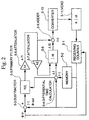
- This PLL device comprises a receiving counter 4-1, which has the same structure as that of the counter at the transmitting side , for counting the standard clock received by the receiving side; a memory 4-2 for storing an output of the receiving counter for a predetermined period; a subtractor 4-3 for comparing between a counted value of the receiving counter 4-1 and the received count value by reading out the counted value of the receiving counter 4-1 whenever the counted value of the counter of the transmitting side is transmitted; a differential time calculator 4-4 for calculating the differential time between the present count value and a preceding count value of the receiving counter 4-1; a first attenuator 4-5 for attenuating the output gain of the subtractor 4-3; a second attenuator 4-6 for further attenuating the output of the first attenuator 4-5; an integrator 4-7 for integrating an output of the second attenuator 4-6 based on the differential time obtained by the differential calculator 4-4; an adder for adding an output of the first attenutor 4-5 to an output
- Fig. 3 shows a construction of the integrator 4-7.
- the secondary type PLL is capable of operating such that the delay element performs corresponding to ⁇ t for the random time information by using ⁇ t as an operator for the integrator 4-7 by calculating ⁇ t from the time difference between the present count T(i) and the preceding count T(i-1).
- the present invention is effective in providing a PLL device having a fixed jitter suppression characteristic, by using ⁇ t obtained from the difference between the present count value T(i) and the preceding count value T(i-1) as the operator for each constituting element for enabling the delay element to operate coping with random time information.
Landscapes
- Engineering & Computer Science (AREA)
- Multimedia (AREA)
- Signal Processing (AREA)
- Stabilization Of Oscillater, Synchronisation, Frequency Synthesizers (AREA)
- Synchronisation In Digital Transmission Systems (AREA)
- Synchronizing For Television (AREA)
- Compression Or Coding Systems Of Tv Signals (AREA)
Applications Claiming Priority (2)
| Application Number | Priority Date | Filing Date | Title |
|---|---|---|---|
| JP35119397A JP3092660B2 (ja) | 1997-12-19 | 1997-12-19 | ランダムな時刻情報から基準クロックを再生するpllとその方法 |
| JP35119397 | 1997-12-19 |
Publications (2)
| Publication Number | Publication Date |
|---|---|
| EP0924862A2 true EP0924862A2 (fr) | 1999-06-23 |
| EP0924862A3 EP0924862A3 (fr) | 2002-11-13 |
Family
ID=18415690
Family Applications (1)
| Application Number | Title | Priority Date | Filing Date |
|---|---|---|---|
| EP19980124050 Withdrawn EP0924862A3 (fr) | 1997-12-19 | 1998-12-17 | PLL servant à la reproduction d'un signal d'horloge standard à partir d'informations de temps aléatoires |
Country Status (5)
| Country | Link |
|---|---|
| US (1) | US6496553B1 (fr) |
| EP (1) | EP0924862A3 (fr) |
| JP (1) | JP3092660B2 (fr) |
| CN (1) | CN1137538C (fr) |
| CA (1) | CA2256583C (fr) |
Cited By (1)
| Publication number | Priority date | Publication date | Assignee | Title |
|---|---|---|---|---|
| EP1875609A4 (fr) * | 2005-04-23 | 2010-07-28 | Nortel Networks Ltd | Methode et appareil pour concevoir un pll |
Families Citing this family (4)
| Publication number | Priority date | Publication date | Assignee | Title |
|---|---|---|---|---|
| US8306170B2 (en) * | 1998-03-31 | 2012-11-06 | International Business Machines Corporation | Digital audio/video clock recovery algorithm |
| US7043651B2 (en) * | 2001-09-18 | 2006-05-09 | Nortel Networks Limited | Technique for synchronizing clocks in a network |
| US6680644B2 (en) * | 2001-09-26 | 2004-01-20 | Siemens Information & Communication Networks, Inc. | Digital interpolation window filter for phase-locked loop operation with randomly jittered reference clock |
| US7835366B2 (en) * | 2005-11-01 | 2010-11-16 | Ciena Corporation | Three-way message exchange clock synchronization |
Family Cites Families (18)
| Publication number | Priority date | Publication date | Assignee | Title |
|---|---|---|---|---|
| JPS6272224A (ja) | 1985-09-25 | 1987-04-02 | Nec Corp | デイジタルpll回路 |
| JPS62298227A (ja) | 1986-06-18 | 1987-12-25 | Hitachi Ltd | デイジタルpll回路 |
| JP2525469B2 (ja) | 1988-11-24 | 1996-08-21 | 日本電気ホームエレクトロニクス株式会社 | ジッタレス光伝送方法 |
| JPH0770995B2 (ja) | 1989-03-14 | 1995-07-31 | 富士通株式会社 | 位相同期ループ |
| JPH03124111A (ja) | 1989-10-09 | 1991-05-27 | Yamaha Corp | ディジタルコントロールドフィルタ |
| JPH0472817A (ja) | 1990-07-12 | 1992-03-06 | Takaya Maruoka | ディジタルpll回路 |
| JPH05268076A (ja) | 1992-03-19 | 1993-10-15 | Fujitsu Ltd | デジタルpll装置 |
| JP3124111B2 (ja) | 1992-06-25 | 2001-01-15 | 三菱重工業株式会社 | 石炭ミル制御装置 |
| JP3085511B2 (ja) * | 1994-11-24 | 2000-09-11 | 株式会社アドバンテスト | 基準周波数発生装置 |
| JPH08161829A (ja) | 1994-12-01 | 1996-06-21 | Canon Inc | デジタル情報再生装置及びデジタルpll装置 |
| JPH08321772A (ja) | 1995-05-24 | 1996-12-03 | Mitsubishi Electric Corp | Pll回路 |
| KR100190996B1 (ko) | 1995-08-09 | 1999-06-15 | 이계철 | 위상 동기회로 |
| JP2891149B2 (ja) * | 1995-11-20 | 1999-05-17 | 日本電気株式会社 | 位相制御ループ方式 |
| JP2692669B2 (ja) | 1995-12-20 | 1997-12-17 | 日本電気株式会社 | クロック生成回路 |
| JPH09191417A (ja) | 1996-01-10 | 1997-07-22 | Victor Co Of Japan Ltd | クロック再生装置 |
| JPH09205564A (ja) | 1996-01-29 | 1997-08-05 | Oki Electric Ind Co Ltd | クロック生成回路 |
| JP3617171B2 (ja) | 1996-03-22 | 2005-02-02 | ソニー株式会社 | エンコーダ装置及び方法、デコーダ装置及び方法、並びに信号伝送方法 |
| JP3767966B2 (ja) | 1997-03-31 | 2006-04-19 | 株式会社日立国際電気 | データ伝送装置 |
-
1997
- 1997-12-19 JP JP35119397A patent/JP3092660B2/ja not_active Expired - Fee Related
-
1998
- 1998-12-11 CN CNB981231993A patent/CN1137538C/zh not_active Expired - Fee Related
- 1998-12-17 EP EP19980124050 patent/EP0924862A3/fr not_active Withdrawn
- 1998-12-18 CA CA 2256583 patent/CA2256583C/fr not_active Expired - Fee Related
- 1998-12-18 US US09/215,339 patent/US6496553B1/en not_active Expired - Lifetime
Cited By (1)
| Publication number | Priority date | Publication date | Assignee | Title |
|---|---|---|---|---|
| EP1875609A4 (fr) * | 2005-04-23 | 2010-07-28 | Nortel Networks Ltd | Methode et appareil pour concevoir un pll |
Also Published As
| Publication number | Publication date |
|---|---|
| JP3092660B2 (ja) | 2000-09-25 |
| CA2256583A1 (fr) | 1999-06-19 |
| US6496553B1 (en) | 2002-12-17 |
| EP0924862A3 (fr) | 2002-11-13 |
| CN1137538C (zh) | 2004-02-04 |
| CA2256583C (fr) | 2002-08-20 |
| CN1220521A (zh) | 1999-06-23 |
| JPH11186906A (ja) | 1999-07-09 |
Similar Documents
| Publication | Publication Date | Title |
|---|---|---|
| US7145488B2 (en) | Method and system for converting digital samples to an analog signal | |
| EP0526573B1 (fr) | Circuit de recouvrement d'horloge sans cretes de sautillement | |
| US4538119A (en) | Clock extraction circuit using an oscillator and phase-locked programmable divider | |
| KR970009688B1 (ko) | 지터 억압회로 | |
| US5576664A (en) | Discrete time digital phase locked loop | |
| CA2256583C (fr) | Circuit de verrouillage de phase servant a reproduire une horloge standard a partir d'une information chronologique aleatoire | |
| JPH07264060A (ja) | デジタル位相ロック回路のループフィルタを制御するための方法、及びそのための装置 | |
| EP0778675B1 (fr) | Circuit numérique de boucle à verrouillage de phase | |
| US7346139B2 (en) | Circuit and method for generating a local clock signal | |
| US5864248A (en) | Phase-locked loop circuit for reproducing clock signals synchronized with transmitter in receiver | |
| JPS60203045A (ja) | 位相同期検波復調器 | |
| US5451944A (en) | Sampling frequency converter by linear interpolation | |
| EP1187374A1 (fr) | Récepteur optique à débit binaire independant | |
| US7321627B2 (en) | Method and system for providing zero detect and auto-mute | |
| JPH0669760A (ja) | 選択呼出し受信機のフィルタ回路 | |
| JP3105574B2 (ja) | 標本化周波数制御方式 | |
| JPH10224336A (ja) | 位相同期回路及び位相同期方法 | |
| JP2723819B2 (ja) | 標本化クロック再生装置 | |
| JPS59110280A (ja) | 水平同期信号処理回路 | |
| US6072848A (en) | Method and apparatus for constructing a digital phase differentiator incorporating a dynamic decrement counter | |
| US5631708A (en) | Automatic phase control apparatus | |
| JP3318899B2 (ja) | クロツク抽出回路 | |
| JPH0897638A (ja) | 高周波デジタル信号受信装置 | |
| JPH05152945A (ja) | 自動周波数・利得制御回路 | |
| JPH11150475A (ja) | シンセサイザ |
Legal Events
| Date | Code | Title | Description |
|---|---|---|---|
| PUAI | Public reference made under article 153(3) epc to a published international application that has entered the european phase |
Free format text: ORIGINAL CODE: 0009012 |
|
| AK | Designated contracting states |
Kind code of ref document: A2 Designated state(s): AT BE CH CY DE DK ES FI FR GB GR IE IT LI LU MC NL PT SE |
|
| AX | Request for extension of the european patent |
Free format text: AL;LT;LV;MK;RO;SI |
|
| PUAL | Search report despatched |
Free format text: ORIGINAL CODE: 0009013 |
|
| AK | Designated contracting states |
Kind code of ref document: A3 Designated state(s): AT BE CH CY DE DK ES FI FR GB GR IE IT LI LU MC NL PT SE |
|
| AX | Request for extension of the european patent |
Free format text: AL;LT;LV;MK;RO;SI |
|
| 17P | Request for examination filed |
Effective date: 20021212 |
|
| 17Q | First examination report despatched |
Effective date: 20030226 |
|
| AKX | Designation fees paid |
Designated state(s): DE FR GB |
|
| STAA | Information on the status of an ep patent application or granted ep patent |
Free format text: STATUS: THE APPLICATION IS DEEMED TO BE WITHDRAWN |
|
| 18D | Application deemed to be withdrawn |
Effective date: 20050812 |