EP0940855A2 - Feldeffekttransistor mit III-V Halbleiterheteroübergang - Google Patents
Feldeffekttransistor mit III-V Halbleiterheteroübergang Download PDFInfo
- Publication number
- EP0940855A2 EP0940855A2 EP99104470A EP99104470A EP0940855A2 EP 0940855 A2 EP0940855 A2 EP 0940855A2 EP 99104470 A EP99104470 A EP 99104470A EP 99104470 A EP99104470 A EP 99104470A EP 0940855 A2 EP0940855 A2 EP 0940855A2
- Authority
- EP
- European Patent Office
- Prior art keywords
- layer
- gaas
- undoped
- algaas
- doped
- Prior art date
- Legal status (The legal status is an assumption and is not a legal conclusion. Google has not performed a legal analysis and makes no representation as to the accuracy of the status listed.)
- Withdrawn
Links
Images












Classifications
-
- H—ELECTRICITY
- H10—SEMICONDUCTOR DEVICES; ELECTRIC SOLID-STATE DEVICES NOT OTHERWISE PROVIDED FOR
- H10D—INORGANIC ELECTRIC SEMICONDUCTOR DEVICES
- H10D30/00—Field-effect transistors [FET]
- H10D30/40—FETs having zero-dimensional [0D], one-dimensional [1D] or two-dimensional [2D] charge carrier gas channels
- H10D30/43—FETs having zero-dimensional [0D], one-dimensional [1D] or two-dimensional [2D] charge carrier gas channels having one-dimensional [1D] charge carrier gas channels, e.g. quantum wire FETs or transistors having 1D quantum-confined channels
-
- H—ELECTRICITY
- H10—SEMICONDUCTOR DEVICES; ELECTRIC SOLID-STATE DEVICES NOT OTHERWISE PROVIDED FOR
- H10D—INORGANIC ELECTRIC SEMICONDUCTOR DEVICES
- H10D30/00—Field-effect transistors [FET]
- H10D30/01—Manufacture or treatment
- H10D30/015—Manufacture or treatment of FETs having heterojunction interface channels or heterojunction gate electrodes, e.g. HEMT
-
- H—ELECTRICITY
- H10—SEMICONDUCTOR DEVICES; ELECTRIC SOLID-STATE DEVICES NOT OTHERWISE PROVIDED FOR
- H10D—INORGANIC ELECTRIC SEMICONDUCTOR DEVICES
- H10D30/00—Field-effect transistors [FET]
- H10D30/40—FETs having zero-dimensional [0D], one-dimensional [1D] or two-dimensional [2D] charge carrier gas channels
- H10D30/47—FETs having zero-dimensional [0D], one-dimensional [1D] or two-dimensional [2D] charge carrier gas channels having two-dimensional [2D] charge carrier gas channels, e.g. nanoribbon FETs or high electron mobility transistors [HEMT]
- H10D30/471—High electron mobility transistors [HEMT] or high hole mobility transistors [HHMT]
- H10D30/473—High electron mobility transistors [HEMT] or high hole mobility transistors [HHMT] having confinement of carriers by multiple heterojunctions, e.g. quantum well HEMT
- H10D30/4732—High electron mobility transistors [HEMT] or high hole mobility transistors [HHMT] having confinement of carriers by multiple heterojunctions, e.g. quantum well HEMT using Group III-V semiconductor material
-
- H—ELECTRICITY
- H10—SEMICONDUCTOR DEVICES; ELECTRIC SOLID-STATE DEVICES NOT OTHERWISE PROVIDED FOR
- H10D—INORGANIC ELECTRIC SEMICONDUCTOR DEVICES
- H10D62/00—Semiconductor bodies, or regions thereof, of devices having potential barriers
- H10D62/10—Shapes, relative sizes or dispositions of the regions of the semiconductor bodies; Shapes of the semiconductor bodies
- H10D62/13—Semiconductor regions connected to electrodes carrying current to be rectified, amplified or switched, e.g. source or drain regions
- H10D62/149—Source or drain regions of field-effect devices
- H10D62/161—Source or drain regions of field-effect devices of FETs having Schottky gates
Definitions
- the present invention relates to an FET (Field Effect Transistor) and more particularly to a hetero junction FET.
- FET Field Effect Transistor
- GaAs FETs are extensively used as high frequency devices.
- a high power device among others, a multi-step recess structure is used to reduce a source resistance and to guarantee a gate breakdown voltage, as taught in, e.g., a paper entitled "High Efficiency Power Module Using HEMT for PDC" presented at the 1996 Conventional of the Electronics Society, the Institute of Electronics and Information Engineers of Japan, Vol. 2, p. 30 (issued August, 30, 1996).
- ON resistance of an FET is the total distributed equivalent resistance from a source electrode to a drain electrode.
- a low ON resistance is essential for implementing a desirable power and a desirable efficiency characteristic at low voltage operation.
- an ON resistance available with conventional FETs is high because a contact resistance from a cap layer to a channel layer is high.
- sheet resistances at an exposed GaAs layer portion and on exposed AlGaAs gate contact layer portion are high, further increasing the ON resistance.
- a third AlGaAs layer is doped with a high concentration n-type impurity.
- a fourth GaAs layer includes an undoped layer contacting the third AlGaAs layer and a layer doped with a high concentration n-type impurity and forming the top of the fourth GaAs layer.
- the second GaAs gate buried layer and a gate electrode contact each other without any gap.
- a multi-recess structure is formed by using, e.g., a GaAs/AlGaAs laminate structure and selective etching.
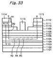
- the FET includes a semi-insulating GaAs substrate 1101.
- an undoped Al 0.2 Ga 0.8 As buffer layer 1102 an Al 0.2 Ga 0.8 As electron supply layer 1103 doped with Si, an undoped Al 0.2 Ga 0.8 As spacer layer 1104, an undoped In 0.2 Ga 0.8 As channel layer 1105, an undoped Al 0.2 Ga 0.8 As spacer layer 1106, an Al 0.2 Ga 0.8 As electron supply layer 1107 doped with Si, an undoped Al 0.2 Ga 0.8 As gate contact layer 1108, a GaAs gate buried layer 1109, an Al 0.2 Ga 0.8 As wide-recess stopper layer 1110 doped with Si, and a GaAs cap layer 1111 doped with Si.
- the GaAs layer 1111 is selectively etched with the wide-recess stopper layer 1110 serving as a stopper layer. Then, after the removal of the mask, a new mask formed with a gate recess pattern is formed. Subsequently, the GaAs layer 1109 is selectively etched with the gate contact layer 1108 playing the role of a stopper layer. In the specific structure shown in FIG. 33, the sides of a gate electrode are spaced from the GaAs layer by relatively great gaps.
- FIG. 33 also shows distributed equivalent resistances in the conventional FET.
- the resistances include a contact resistance R1 from the ohmic electrode to the cap layer, a contact resistance R2 from the cap layer to the channel layer, a sheet resistance R3 at a portion where the gate buried GaAs layer is exposed, a sheet resistance R4 at a portion where the AlGaAs gate contact layer is exposed, and a sheet resistance R5 beneath the gate electrode.
- the ON resistance of the FET should be low for the reason stated earlier.
- FIG. 34 shows a conduction band profile in a direction X11-Y11 shown in FIG. 33.
- the high contact resistance is ascribable to the fact that the AlGaAs stopper layer used to form the multi-step recess structure has a high potential barrier, limiting the tunnel probability from the cap layer to the channel layer.
- Another problem is that when the AlGaAs stopper layer is removed after the formation of the wide recess, the distance between the exposed GaAs surface and the channel beneath it is reduced, increasing the sheet resistance R3 and therefore the ON resistance is high. This is because a depletion layer extends from the exposed GaAs layer surface toward the channel layer and causes electrons in the channel to be depleted.
- a further problem is that because the sides of the gate electrode do not contact the GaAs layer, the AlGaAs gate contact layer is exposed to the outside at the sides of the gate electrode. As a result, electrons in the channel layer are also depleted by a surface depletion layer extending from the AlGaAs gate contact layer.
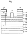
- an FET embodying the present invention includes a semi-insulating GaAs substrate 101. As shown, there are sequentially formed on the substrate 101 a 400 nm thick undoped GaAs buffer layer 102, a 100 nm thick undoped Al 0.2 Ga 0.8 As buffer layer 103, a 4 nm thick Al 0.2 Ga 0.8 As electron supply layer 104 doped with 4 x 10 18 cm -3 of Si, a 2 nm thick undoped Al 0.2 Ga 0.8 As spacer layer 105, a 15 nm thick undoped In 0.2 Ga 0.8 As channel layer 106, a 2 nm thick undoped Al 0.2 Ga 0.8 As spacer layer 107, a 9 nm thick Al 0.2 Ga 0.8 As electron supply layer 108 doped with 4 x 10 18 cm -3 of Si, a 10 nm thick undoped Al 0.2 Ga 0.8 As gate contact layer 109, a 30 nm thick GaAs gate
- a mask formed with a recess pattern is formed on the wafer.
- the GaAs layers 113 and 112 are selectively etched with the wide-recess stopper layer 111 serving as a stop layer.
- dry etching using an ECR (Electron Cyclotron Resonance) etching system or an RIE (Reactive Ion Etching) system and a mixture of chloride gas containing only chlorine as a halogen element and fluoride gas containing only fluorine, e.g., a BCl 3 and SF 6 mixture.
- the GaAs gate buried layer 110 is selectively etched via a new mask formed with agate recess pattern with the gate contact layer 109 serving as a stopper layer. As a result, the undoped gate contact layer 109 is exposed to the outside. At this instant, the buried layer 110 is not overetched. A gate electrode 114 is formed on the exposed gate contact layer 109. This produces a structure in which no gaps are present at the sides of the gate electrode 114.
- a source electrode 115 and a drain electrode 116 are formed by the evaporation lift-off and alloying (e.g. 400°C/1 min) of AuGe, serving as ohmic electrodes.
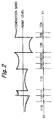
- FIG. 2 shows a conduction band profile in a direction X1-Y1 of FIG. 1.
- the conduction band profile of a conventional structure lacking the undoped GaAs layer 112 on the wide-recess stopper layer 111 is indicated by a dashed line in FIG. 2.
- two-dimensional electron gas formed in the undoped GaAs layer 112 lowers the potential barrier and thereby increases the probability that electrons pass through the potential barrier of the stopper layer 111.
- the scattering by ionized impurities is suppressed and electron ability is high in the layer 112. Consequently, the contact resistance from the cap layer 113 to the channel layer 106 is successfully reduced. Further, the increase of this sheet resistance is suppressed because the gate contact layer 109 is not exposed to the outside.
- FIG. 3 A second embodiment of the FET in accordance with the present invention is shown in FIG. 3 and includes a semi-insulating GaAs substrate 201. As shown, there are sequentially formed on the substrate 201 a 400 nm thick undoped GaAs buffer layer 202, a 100 nm thick undoped Al 0.2 Ga 0.8 As buffer layer 203, a 4 nm thick Al 0.2 Ga 0.8 As electron supply layer 204 doped with 4 x 10 18 cm -3 of Si, a 2 nm thick undoped Al 0.2 Ga 0.8 As spacer layer 205, a 15 nm thick undoped In 0.2 Ga 0.8 As channel layer 206, a 2 nm thick undoped Al 0.2 Ga 0.8 As spacer layer 207, a 9 nm thick Al 0.2 Ga 0.8 As electron supply layer 208 doped with 4 x 10 18 cm -3 of Si, a 10 nm thick undoped Al 0.2 Ga 0.8 As gate contact layer 209, a 24 nm
- a mask formed with a wide recess pattern is formed on the above epitaxial wafer. Then, the GaAs layers 214 and 213 are selectively etched with the wide-recess stopper layer 212 serving as a stop layer. To so etch the two layers 214 and 213, there may be used dry etching using a mixture of chloride gas containing only chlorine as a halogen element and fluoride gas containing only fluorine, e.g., a BCl 6 and SF 6 mixture.
- the undoped GaAs layer 211 and GaAs gate buried layer 210 are selectively etched via a new mask formed with a gate recess pattern with the gate contact layer 209 serving as a stopper layer.
- the undoped gate contact layer 209 is exposed to the outside.
- the buried layer 212 is not overetched.
- a gate electrode 215 is formed on the exposed gate contact layer 209. This produces a structure in which no gaps are present at the sides of the gate electrode 215.
- a source electrode 216 and a drain electrode 217 are formed by the evaporation lift-off and alloying (e.g. 400°C/1 min) of AuGe, serving as ohmic electrodes.
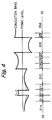
- FIG. 4 shows a conduction band profile in a direction X2-Y2 of FIG. 3.
- the conduction band profile of a conventional structure lacking the undoped GaAs layers 213 and 211 respectively present on the top and bottom of the wide-recess stopper layer 212 is indicated by a dashed line in FIG. 2.
- two-dimensional electron gas formed in the undoped GaAs layers 213 and 211 lowers the potential barrier and thereby increases the probability that electrons pass through the potential barrier of the stopper layer 212.
- the scattering by ionized impurities is suppressed and electron mobility is high in the layers 213 and 211. Consequently, the contact resistance from the cap layer 214 to the channel layer 206 is successfully reduced. Further, the increase of this sheet resistance is suppressed because the gate contact layer 209 is not exposed to the outside.
- FIG. 5 A third embodiment of the FET in accordance with the present invention is shown in FIG. 5 and includes a semi-insulating GaAs substrate 301. As shown, there are sequentially formed on the substrate 301 a 400 nm thick undoped GaAs buffer layer 302, a 100 nm thick undoped Al 0.2 Ga 0.8 As buffer layer 303, a 4 nm thick Al 0.2 Ga 0.8 As electron supply layer 304 doped with 4 x 10 18 cm -3 of Si, a 2 nm thick undoped Al 0.2 Ga 0.8 As spacer layer 305, a 15 nm thick undoped In 0.2 Ga 0.8 As channel layer 306, a 2 nm thick undoped Al 0.2 Ga 0.8 As spacer layer 307, a 9 nm thick Al 0.2 Ga 0.8 As electron supply layer 308 doped with 4 x 10 18 cm -3 of Si, a 10 nm thick Al 0.2 Ga 0.8 As gate contact layer 309 doped with 4 x 10 18 cm -3 of
- a mask formed with a wide recess pattern is formed on the above epitaxial wafer. Then, the GaAs layer 313 is selectively etched with the wide-recess stopper layer 312 serving as a stopper layer. To so etch the GaAs layer 313, there may be used dry etching using a mixture of chloride gas containing only chlorine as a halogen element and fluoride gas containing only fluorine, e.g., a BCl 6 and SF 6 mixture.
- the GaAs layers 311 and 310 are selectively etched via a new mask formed with a gate recess pattern with the gate contact layer 309 serving as a stopper layer. As a result, the gate contact layer 309 is exposed to the outside. At this instant, the gate buried layers 311 and 310 are not overetched. A gate electrode 314 is formed on the exposed gate contact layer 309. This produces a structure in which no gaps are present at the sides of the gate electrode 314.
- a source electrode 315 and a drain electrode 316 are formed by the evaporation lift-off and alloying (e.g. 400°C/1 min) of AuGe, serving as ohmic electrodes.
- FIG. 6 shows a conduction band profile in a direction X3-Y3 of FIG. 5.
- the conduction band profile of a conventional structure including an undoped gate contact layer, but lacking the undoped GaAs layer 310 is indicated by a dashed line in FIG. 6.
- two-dimensional electron gas formed in the undoped GaAs layer 310 lowers the potential barrier and thereby increases the probability that electrons pass through the potential barrier formed by the Al 0.2 Ga 0.8 As layers 309, 308 and 307.
- the scattering by ionized impurities is suppressed and electron mobility is high in the layer 310.
- the contact resistance from the cap layer 313 to the channel layer 306 is successfully reduced.
- two-dimensional electron gas formed in the undoped GaAs layer 310 having high electron mobility forms a low resistance current path (P2, FIG. 5) in addition to a current path (P1, FIG. 5) formed in the channel layer 306.
- the current path P2 serves to reduce the sheet resistance of the portion (S, FIG. 5) where the GaAs gate buried layer is exposed to the outside.
- the gate contact layer 309 is not exposed to the outside, the sheet resistance at this portion sparingly increases.
- a fourth embodiment of the FET in accordance with the present invention is shown in FIG. 7 and includes a semi-insulating GaAs substrate 401. As shown, there are sequentially formed on the substrate 401 a 400 nm thick undoped GaAs buffer layer 402, a 100 nm thick undoped Al 0.2 Ga 0.8 As buffer layer 403, a 4 nm thick Al 0.2 Ga 0.8 As electron supply layer 404 doped with 4 x 10 18 cm -3 of Si, a 2 nm thick undoped Al 0.2 Ga 0.8 As spacer layer 405, a 15 nm thick undoped In 0.2 Ga 0.8 As channel layer 406, a 2 nm thick undoped Al 0.2 Ga 0.8 As spacer layer 407, a 9 nm thick Al 0.2 Ga 0.8 As electron supply layer 408 doped with 4 x 10 18 cm -3 of Si, a 10 nm thick Al 0.2 Ga 0.8 As gate contact layer 409 doped with 5 x 10 17 cm -3 of Si, a 6
- a mask formed wide a wide recess pattern is formed on the above epitaxial wafer. Then, the GaAs layers 414 and 413 are selectively etched with the wide-recess stopper layer 412 serving as a stopper layer. To so etch the GaAs layers 414 and 413, there may be used dry etching using a mixture of chloride gas containing only chlorine as a halogen element and fluoride gas containing only fluorine, e.g., a BCl 3 and SF 6 mixture.
- the GaAs layers 411 and 410 are selectively etched via a new mask formed with a gate recess pattern with the gate contact layer 409 serving as a stopper layer. As a result, the gate contact layer 409 is exposed to the outside. At this instant, the gate buried layers 411 and 410 are not overetched. A gate electrode 414 is formed on the exposed gate contact layer 409. This produces a structure in which no gaps are present at the sides of the gate electrode 414.
- a source electrode 416 and a drain electrode 417 are formed by the evaporation lift-off and alloying (e.g. 400°C/1 min) of AuGe, serving as ohmic electrodes.
- FIG. 8 shows a conduction band profile in a direction X4-Y4 of FIG. 7.
- the conduction band profile of a conventional structure including an undoped gate contact layer, but lacking the undoped GaAs layers 410 and 413 is indicated by a dashed line in FIG. 8. As shown, in the structure shown in FIG.
- two-dimensional electron gas formed in the undoped GaAs layers 410 and 413 lowers the potential barrier and thereby increases the probability that electrons pass through the potential barrier of the Al 0.2 Ga 0.8 As layer 412 and a potential barrier formed by the Al 0.2 Ga 0.8 As layers 409, 408 and 407,
- the scattering by ionized impurities is suppressed and electron mobility is high in the layers 410 and 413. Consequently, the contact resistance from the cap layer 414 to the channel layer 406 is successfully reduced.
- two-dimensional electron gas formed in the undoped GaAs layer 410 having great electron mobility forms a low resistance current path (P2, FIG.
- the current path P2 serves to reduce the sheet resistance of the portion (S, FIG. 7) where the GaAs gate buried layer is exposed to the outside. In addition, because the gate contact layer 409 is not exposed to the outside, the sheet resistance at this portion sparingly increases.
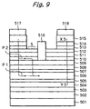
- a fifth embodiment of the FET in accordance with the present invention is shown in FIG. 9 and includes a semi-insulating GaAs substrate 501. As shown, there are sequentially formed on the substrate 501 a 400 nm thick undoped GaAs buffer layer 502, a 100 nm thick undoped Al 0.2 Ga 0.8 As buffer layer 503, a 4 nm thick Al 0.2 Ga 0.8 As electron supply layer 504 doped with 4 x 10 18 cm -3 of Si, a 2 nm thick undoped Al 0.2 Ga 0.8 As spacer layer 505, a 15 nm thick undoped In 0.2 Ga 0.8 As channel layer 506, a 2 nm thick undoped Al 0.2 Ga 0.8 As spacer layer 507, a 9 nm thick Al 0.2 Ga 0.8 As electron supply layer 508 doped with 4 x 10 18 cm -3 of Si, a 10 nm thick Al 0.2 Ga 0.8 As gate contact layer 509 doped with 5 x 10 17 cm -3 of Si, a 6
- a mask formed with a wide recess pattern is formed on the above epitaxial wafer. Then, the GaAs layers 515 and 514 are selectively etched with the wide-recess stopper layer 513 serving as a stopper layer. To so etch the GaAs layers 515 and 514, there may be used dry etching using a mixture of chloride gas containing only chlorine as a halogen element and fluoride gas containing only fluorine, e.g., a BCl 3 and SF 6 mixture.
- the GaAs layers 512, 511 and 510 are selectively etched via a new mask formed with a gate recess pattern with the gate contact layer 509 serving as a stopper layer.
- the gate contact layer 509 is exposed to the outside.
- the gate buried layers 512, 511 and 510 are not overetched.
- a gate electrode 516 is formed on the exposed gate contact layer 509. This produces a structure in which no gaps are present at the sides of the gate electrode 516.
- a source electrode 517 and a drain electrode 518 are formed by the evaporation lift-off and alloying (e.g. 400°C/1 min) of AuGe, serving as ohmic electrodes.
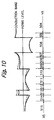
- FIG. 10 shows a conduction band profile in a direction X5-Y5 of FIG. 9.
- the conduction band profile of a conventional structure including an undoped gate contact layer, but lacking the undoped GaAs layers 510, 512 and 514 is indicated by a dashed line in FIG. 10.
- two-dimensional electron gas formed in the undoped GaAs layers 510, 512 and 514 lowers the potential barrier and thereby increases the probability that electrons pass through the potential barrier of the Al 0.2 Ga 0.8 As layer 513 and a potential barrier formed by the Al 0.2 Ga 0.8 As layers 509, 508 and 507.
- the scattering by ionized impurities is suppressed and electron mobility is high in the layers 510, 512 and 514. Consequently, the contact resistance from the cap layer 515 to the channel layer 506 is successfully reduced.
- two-dimensional electron gas formed in the undoped GaAs layer 510 having great electron mobility forms a low resistance current path (P2, FIG. 9) in addition to a current path (P1, FIG. 9) formed in the channel layer 506.
- the current path P2 serves to reduce the sheet resistance of the portion (S, FIG. 9) where the GaAs gate buried layer is exposed to the outside. In addition, because the gate contact layer 509 is not exposed to the outside, the sheet resistance increase of this portion is suppressed.
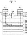
- a sixth embodiment of the FET in accordance with the present invention is shown in FIG. 11 and includes a semi-insulating GaAs substrate 601. As shown, there are sequentially formed on the substrate 601 a 400 nm thick undoped GaAs buffer layer 602, a 100 nm thick undoped Al 0.2 Ga 0.8 As buffer layer 603, a 4 nm thick Al 0.2 Ga 0.8 As electron supply layer 604 doped with 4 x 10 18 cm -3 of Si, a 2 nm thick undoped Al 0.2 Ga 0.8 As spacer layer 605, a 15 nm thick undoped In 0.2 Ga 0.8 As channel layer 606, a 2 nm thick undoped Al 0.2 Ga 0.8 As spacer layer 607, a 9 nm thick Al 0.2 Ga 0.8 As electron supply layer 608 doped with 4 x 10 18 cm -3 of Si, a 25 nm thick Al 0.2 Ga 0.8 As gate contact layer 609 doped with 5 x 10 17 cm -3 of Si, a 15
- a mask formed with a wide recess pattern is formed on the above epitaxial wafer. Then, the GaAs layers 613 and 612 are selectively etched with the wide-recess stopper layer 611 serving as a stopper layer. To so etch the GaAs layers 613 and 612, there may be used dry etching using a mixture of chloride gas containing only chlorine as a halogen element and fluoride gas containing only fluorine, e.g., a BCl 3 and SF 6 mixture.
- the GaAs layer 610 is selectively etched via a new mask formed with a gate recess pattern with the gate contact layer 609 serving as a stopper layer. As a result, the gate contact layer 609 is exposed to the outside. At this instant, the gate buried layer 610 is not overetched. A gate electrode 614 is formed on the exposed gate contact layer 609. This produces a structure in which no gaps are present at the sides of the gate electrode 614.
- a source electrode 615 and a drain electrode 616 are formed by the evaporation lift-off and alloying (e.g. 400°C/1 min) of AuGe, serving as ohmic electrodes.
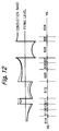
- FIG. 12 shows a conduction band profile in a direction X6-Y6 of FIG. 11.
- the conduction band profile of a conventional structure including an undoped gate contact layer and the GaAs layer 610 doped with an n-type impurity, but lacking the undoped GaAs layer 612 is indicated by a dashed line in FIG. 12.
- two-dimensional electron gas formed in the undoped GaAs layers 610 and 612 lowers the potential barrier and thereby increases the probability that electrons pass through the potential barrier of the Al 0.2 Ga 0.8 As layer 611 and a potential barrier formed by the Al 0.2 Ga 0.8 As layers 609, 608 and 607.
- the scattering by ionized impurities is suppressed and electron mobility is high in the layers 612 and 610. Consequently, the contact resistance from the cap layer 614 to the channel layer 606 is successfully reduced.
- two-dimensional electron gas formed in the undoped GaAs layer 610 having high electron mobility forms a low resistance current path (P2, FIG. 11) in addition to a current path (P1, FIG. 11) formed in the channel layer 606.
- the current path P2 serves to reduce the sheet resistance of the portion (S, FIG. 11) where the GaAs gate buried layer is exposed to the outside. In addition, because the gate contact layer 609 is not exposed to the outside, the sheet resistance increase of this portion is suppressed.
- a seventh embodiment of the FET in accordance with the present invention is shown in FIG. 13 and includes a semi-insulating GaAs substrate 701.
- a 400 nm thick undoped GaAs buffer layer 702 a 100 nm thick undoped Al 0.2 Ga 0.8 As buffer layer 703, a 4 nm thick Al 0.2 Ga 0.8 As electron supply layer 704 doped with 4 x 10 18 cm -3 of Si, a 2 nm thick undoped Al 0.2 Ga 0.8 As spacer layer 705, a 15 nm thick undoped In 0.2 Ga 0.8 As channel layer 706, a 2 nm thick undoped Al 0.2 Ga 0.8 As spacer layer 707, a 9 nm thick Al 0.2 Ga 0.8 As electron supply layer 708 doped with 4 x 10 18 cm -3 of Si, a 10 nm thick undoped Al 0.2 Ga 0.8 As gate contact layer 709, a 20 nm thick GaAs gate buried layer 7
- a mask formed with a wide recess pattern is formed on the above epitaxial wafer. Then, the GaAs layers 715 and 714 are selectively etched with the wide-recess stopper layer 713 serving as a stopper layer. To so etch the GaAs layers 715 and 714, there may be used dry etching using a mixture of chloride gas containing only chlorine as a halogen element and fluoride gas containing only fluorine, e.g., a BCl 3 and SF 6 mixture.
- the GaAs layers 712, 711 and 710 are selectively etched via a new mask formed with a gate recess pattern with the gate contact layer 709 serving as a stopper layer.
- the gate contact layer 709 is exposed to the outside.
- the gate buried layers 712, 711 and 710 are not overetched.
- a gate electrode 716 is formed on the exposed gate contact layer 709. This produces a structure in which no gaps are present at the sides of the gate electrode 716.
- a source electrode 717 and a drain electrode 718 are formed by the evaporation lift-off and alloying (e.g. 400°C/1 min) of AuGe, serving as ohmic electrodes.
- FIG. 14 shows a conduction band profile in a direction X7-Y7 of FIG. 13.
- the conduction band profile of a conventional structure lacking a GaAs layer doped with a high concentration, n-type impurity is indicated by a dashed line in FIG. 14.
- a depletion layer tending to extend from the surface of the GaAs layer 712 toward the channel side stops in the GaAs layers 712, 711 and 710. This is successful to obstruct the rise of a conduction band at the surface side in the channel, so that a great amount of electrons can be stored in the above layer.
- a current path is formed not only in the channel (P1, FIG. 13) but also in the gate buried layer (P2, FIG. 13), so that the sheet resistance is reduced in the exposed portion of the GaAs gate buried layer (S, FIG. 13).
- two-dimensional electron gas formed in the undoped GaAs layer 714 lowers the potential barrier of the Al 0.2 Ga 0.8 As layer 713 and thereby increases the probability that electrons pass through the potential barrier of the Al 0.2 Ga 0.8 As layer 713.
- the scattering by ionized impurities is suppressed and electron mobility is high in the layer. Consequently, the contact resistance from the cap layer 715 to the channel layer 706 is successfully reduced.
- the gate contact layer 709 is not exposed to the outside, the sheet resistance increase of this portion is suppressed.
- FIG. 15 An eighth embodiment of the FET in accordance with the present invention is shown in FIG. 15 and includes a semi-insulating GaAs substrate 801. As shown, there are sequentially formed on the substrate 801 a 400 nm thick undoped GaAs buffer layer 802, a 100 nm thick undoped Al 0.2 Ga 0.8 As buffer layer 803, a 4 nm thick Al 0.2 Ga 0.8 As electron supply layer 804 doped with 4 x 10 18 cm -3 of Si, a 2 nm thick undoped Al 0.2 Ga 0.8 As spacer layer 805, a 15 nm thick undoped In 0.2 Ga 0.8 As channel layer 806, a 2 nm thick undoped Al 0.2 Ga 0.8 As spacer layer 807, a 9 nm thick Al 0.2 Ga 0.8 As electron supply layer 808 doped with 4 x 10 18 cm -3 of Si, a 10 nm thick undoped Al 0.2 Ga 0.8 As gate contact layer 809, a 18 nm thick GaAs gate
- a mask formed with a wide recess pattern is formed on the above epitaxial wafer. Then, the GaAs layers 815 and 814 are selectively etched with the wide-recess stopper layer 813 serving as a stopper layer. To so etch the GaAs layers 815 and 814, there may be used dry etching using a mixture of chloride gas containing only chlorine as a halogen element and fluoride gas containing only fluorine, e.g., a BCl 3 and SF 6 mixture.
- the GaAs layers 812, 811 and 810 are selectively etched via a new mask formed with a gate recess pattern with the gate contact layer 809 serving as a stopper layer.
- the gate contact-layer 809 is exposed to the outside.
- the gate buried layers 812, 811 and 810 are not overetched.
- a gate electrode 816 is formed on the exposed gate contact layer 809. This produces a structure in which no gaps are present at the sides of the gate electrode 816.
- a source electrode 817 and a drain electrode 818 are formed by the evaporation lift-off and alloying (e.g. 400°C/1 min) of AuGe, serving as ohmic electrodes.
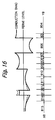
- FIG. 16 shows a conduction band profile in a direction X8-Y8 of FIG. 15.
- the conduction band profile of a conventional structure lacking the undoped GaAs layers 814 and 812 and GaAs layer 811 doped with a high concentration, n-type impurity is indicated by a dashed line in FIG. 15.
- the high concentration doping of the GaAs layer 811 stops the extension of a depletion layer from the surface of the GaAs layer 812 in the GaAs layers 812, 811 and 810.
- two-dimensional electron gas formed in the undoped GaAs layers 812 and 814 lowers the potential barrier and thereby increases the probability that electrons pass through the potential barrier of the Al 0.2 Ga 0.8 As layer 813.
- the scattering by ionized impurities is suppressed and electron is high in the layers 812 and 814. Consequently, the contact resistance from the cap layer 815 to the channel layer 806 is successfully reduced.
- the gate contact layer 809 is not exposed to the outside, the sheet resistance increase of this portion is suppressed.
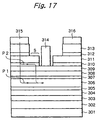
- a ninth embodiment of the FET in accordance with the present invention is shown in FIG. 17 and includes a semi-insulating GaAs substrate 901.
- a 400 nm thick undoped GaAs buffer layer 902 a 100 nm thick undoped Al 0.2 Ga 0.8 As buffer layer 903, a 4 nm thick Al 0.2 Ga 0.8 As electron supply layer 904 doped with 4 x 10 18 cm -3 of Si, a 2 nm thick undoped Al 0.2 Ga 0.8 As spacer layer 905, a 15 nm thick undoped In 0.2 Ga 0.8 As channel layer 906, a 2 nm thick undoped Al 0.2 Ga 0.8 As spacer layer 907, a 9 nm thick Al 0.2 Ga 0.8 As electron supply layer 908 doped with 4 x 10 18 cm -3 of Si, a 10 nm thick Al 0.2 Ga 0.8 As gate contact layer 909 doped with 5 x 10 17 cm -3 of Si, a 15 nn
- a mask formed with a wide recess pattern is formed on the above epitaxial wafer. Then, the GaAs layers 915 and 914 are selectively etched with the wide-recess stopper layer 913 serving as a stopper layer. To so etch the GaAs layers 815 and 814, there may be used dry etching using a mixture of chloride gas containing only chlorine as a halogen element and fluoride gas containing only fluorine, e.g., a BCl 3 and SF 6 mixture.
- the GaAs layers 912, 911 and 910 are selectively etched via a new mask formed with a gate recess pattern with the gate contact layer 909 serving as a stopper layer.
- the gate contact layer 909 is exposed to the outside.
- the gate buried layers 912, 911 and 910 are not overetched.
- a gate electrode 916 is formed on the exposed gate contact layer 909. This produces a structure in which no gaps are present at the sides of the gate electrode 916.
- a source electrode 917 and a drain electrode 918 are formed by the evaporation lift-off and alloying (e.g. 400°C/1 min) of AuGe, serving as ohmic electrodes.
- the high concentration doping of the GaAs layer 911 stops the extension of a depletion layer from the surface of the GaAs layer 912 in the GaAs layers 912, 911 and 910. This is successful to obstruct the rise of a conduction band at the surface side in the channel right below the exposed GaAs layer, so that a great amount of electrons can be stored in the above layer. Further, two-dimensional electron gas is formed in the GaAs layer 910. This, coupled with the fact that the GaAs layer 910 is undoped, reduces diffusion and therefore enhances mobility. A low resistance current path (P2, FIG. 17) is formed by the undoped GaAs layer 910 in addition to a current path (P1, FIG. 17) formed by the channel layer 906. Consequently , the sheet resistance is reduced in the portion where the GaAs gate buried layer 912 is exposed (S, FIG. 17).
- two-dimensional electron gas formed in the undoped GaAs layers 910 and 914 lowers the potential barrier and thereby increases the probability that electrons pass through the potential barrier of the Al 0.2 Ga 0.8 As layer 913 and a potential barrier formed by the Al 0.2 Ga 0.8 As layers 909, 908 and 907. Because electron mobility in the undoped GaAs layers 910 and 914 is high, the contact resistance from the cap layer 915 to the channel layer 906 is lowered. In addition, because the gate contact layer 909 is not exposed to the outside, the sheet resistance increase of this portion is suppressed.
- a tenth embodiment of the FET in accordance with the present invention is shown in FIG. 18 and includes a semi-insulating GaAs substrate 1001.
- a 400 nm thick undoped GaAs buffer layer 1002 a 100 nm thick undoped Al 0.2 Ga 0.8 As buffer layer 1003, a 4 nm thick Al 0.2 Ga 0.8 As electron supply layer 1004 doped with 4 x 10 18 cm -3 of Si, a 2 nm thick undoped Al 0.2 Ga 0.8 As spacer layer 1005, a 15 nm thick undoped In 0.2 Ga 0.8 As channel layer 1006, a 2 nm thick undoped Al 0.2 Ga 0.8 As spacer layer 1007, a 9 nm thick Al 0.2 Ga 0.8 As electron supply layer 1008 doped with 4 x 10 18 cm -3 of Si, a 10 nm thick Al 0.2 Ga 0.8 As gate contact layer 1009 doped with 5 x 10 17 cm -3 of Si, a 15
- a mask formed with a wide recess pattern is formed on the above epitaxial wafer. Then, the GaAs layers 1015 and 1014 are selectively etched with the wide-recess stopper layer 1013 serving as a stopper layer. To so etch the GaAs layers 1015 and 104, there may be used dry etching using a mixture of chloride gas containing only chlorine as a halogen element and fluoride gas containing only fluorine, e.g., a BCl 3 and SF 6 mixture.
- the GaAs layers 1012, 1011 and 1010 are selectively etched via anew mask formed with a gate recess pattern with the gate contact layer 1009 serving as a stopper layer.
- the gate contact layer 1009 is exposed to the outside.
- the gate buried layers 1012, 1011 and 1010 are not overetched.
- a gate electrode 1016 is formed on the exposed gate contact layer 1009. This produces a structure in which no gaps are present at the sides of the gate electrode 1016.
- a source electrode 1017 and a drain electrode 1018 are formed by the evaporation lift-off and alloying (e.g. 400°C/1 min) of AuGe, serving as ohmic electrodes.
- the high concentration doping of the GaAs layer 1011 stops the extension of a depletion layer from the surface of the GaAs layer 1012 in the GaAs layers 1012, 1011 and 1010. This is successful to obstruct the rise of a conduction band at the surface side in the channel right below the exposed GaAs layer 1012, so that a great amount of electrons can be stored in the above layer. Further, two-dimensional electron gas is formed in the GaAs layer 1010. This, coupled with the fact that the GaAs layer 1010 is undoped, reduces diffusion and therefore enhances mobility. A low resistance current path (P2, FIG. 18) is formed by the undoped GaAs layer 1010 in addition to a current path (P1, FIG. 18) formed by the channel layer 1006. Consequently the sheet resistance is reduced in the portion where the GaAs gate buried layer 1012 is exposed (S, FIG. 18).
- two-dimensional electron gas formed in the undoped GaAs layers 1010, 1012 and 1014 lowers the potential barrier and thereby increases the probability that electrons pass through the potential barrier of the Al 0.2 Ga 0.8 As layer 1013 and a potential barrier formed by the Al 0.2 Ga 0.8 As layers 1009, 1008 and 1007. Because electron mobility in the undoped GaAs layers 1010, 1012 and 1014 is high, the contact resistance from the cap layer 1015 to the channel layer 1006 is lowered. In addition, because the gate contact layer 1009 is not exposed to the outside, the sheet resistance increase of this portion is suppressed.
- FIG. 19 shows an eleventh embodiment of the FET in accordance with the present invention.
- This embodiment uses the epitaxial wafer produced in the first embodiment.
- the GaAs layers 113 and 112 are selectively etched with the wide-recess stopper layer 111 serving as a stop layer.
- the two layers 113 and 112 there may be used dry etching using the ECR etching system or the RIE system and a mixture of chloride gas containing only chlorine as a halogen element and fluoride gas containing only fluorine, e.g., a BCl 3 and SF 6 mixture.
- the GaAs gate buried layer 110 is selectively etched via a new mask formed with a gate recess pattern with the gate contact layer 109 serving as a stopper layer. As a result the undoped gate contact layer 109 is exposed to the outside. At this instant, the buried layer 110 is overetched in order to cause etching to proceed in the horizontal direction of the gate buried layer 110.
- the gate electrode 114 is formed on the exposed gate contact layer 109, gaps are formed at the sides of the gate electrode 114. For example, when 100 % overetching was effected by using a BCl 3 and SF 6 gas mixture, gaps of about 20 nm were formed at the sides of the gate electrode 114. Such gaps should preferably be about 10 nm to about 50 nm.
- the source electrode 115 and drain electrode 116 are formed by the evaporation lift-off and alloying (e.g. 400°C/1 min) of AuGe, serving as ohmic electrodes.
- two-dimensional electron gas formed in the undoped GaAs layer 112 lowers the potential barrier and thereby increases the probability that electrons pass through the potential barrier of the stopper layer 111.
- the scattering by ionized impurities is suppressed and electron mobility is hig in the layer. Consequently, the contact resistance from the cap layer 113 to the channel layer 106 is successfully reduced.
- an ON resistance as low as 1.5 ⁇ mm was achieved. This ON resistance is lower than the ON resistance of conventional FETs by 0.1 ⁇ mm.
- a gate breakdown voltage of 15 V was achieved because of the gaps formed at the sides of the gate electrode 114.
- FIG. 20 shows a twelfth embodiment of the FET in accordance with the present invention. This embodiment executes the process of the eleventh embodiment by using the epitaxial layer of the second embodiment. As shown, gaps are formed at the sides of the gate electrode 215.
- two-dimensional electron gas formed in the undoped GaAs layers 213 and 211 lowers the potential barrier and thereby increases the probability that electrons pass through the potential barrier of the stopper layer 212.
- the scattering by ionized impurities is suppressed and electron mobility is high in the layers 213 and 211. Consequently, the contact resistance from the cap layer 214 to the channel layer 206 is successfully reduced.
- an ON resistance as low as 1.2 ⁇ mm was achieved. This ON resistance is lower than the ON resistance of conventional FETs by 0.2 ⁇ mm.
- a gate breakdown voltage of 15 V was achieved because of the gaps formed at the sides of the gate electrode 215.
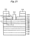
- FIG. 21 shows a thirteenth embodiment of the FET in accordance with the present invention. This embodiment executes the process of the eleventh embodiment by using the epitaxial wafer of the third embodiment. As shown, gaps are formed at the sides of the gate electrodes 314.
- two-dimensional electron gas formed in the undoped GaAs layer 310 lowers the potential barrier and thereby increases the probability that electrons pass through the potential barrier formed by the Al 0.2 Ga 0.8 As layers 309, 308 and 307.
- the scattering by ionized impurities is suppressed and electron mobility is high in the layer. Consequently, the contact resistance from the cap layer 313 to the channel layer 306 is successfully reduced.
- two-dimensional electron gas formed in the undoped GaAs layer 310 having high electron mobility forms a low resistance current path (P2, FIG. 21) in addition to a current path (P1, FIG. 21) formed in the channel layer 306.
- the current path P2 serves to reduce the sheet resistance of the portion (S, FIG. 21) where the GaAs gate buried layer is exposed to the outside.
- an ON resistance as low as 1.4 ⁇ mm was achieved. This ON resistance is lower than the ON resistance of conventional FETs by 0.2 ⁇ mm. Also, a gate breakdown voltage of 15 V was achieved because of the gaps formed at the sides of the gate electrode 314.
- FIG. 22 shows a fourteenth embodiment of the FET in accordance with the present invention. This embodiment executes the process of FIG. 11 by using the epitaxial wafer of the fourth embodiment. As shown, gaps are formed at the sides of the gate electrode 415.
- two-dimensional electron gas formed in the undoped GaAs layers 410 and 413 lowers the potential barrier and thereby increases the probability that electrons pass through the potential barrier of the Al 0.2 Ga 0.8 As layer 412 and a potential barrier formed by the Al 0.2 Ga 0.8 As layers 409, 408 and 407.
- the scattering by ionized impurities is suppressed and electron mobility is high in the layers 410 and 413. Consequently, the contact resistance from the cap layer 414 to the channel layer 406 is successfully reduced.
- two-dimensional electron gas formed in the undoped GaAs layer 410 having great electron mobility forms a low resistance current path (P2, FIG. 22) in addition to a current path (P1, FIG. 22) formed in the channel layer 406.
- the current path P2 serves to reduce the sheet resistance of the portion (S, FIG. 22) where the GaAs gate buried layer is exposed to the outside.
- an ON resistance as low as 1.3 ⁇ mm was achieved. This ON resistance is lower than the ON resistance of conventional FETs by 0.3 ⁇ mm. Also, a gate breakdown voltage of 15 V was achieved because of the gaps formed at the sides of the gate electrode 415.
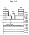
- FIG. 23 shows a fifteenth embodiment of the FET in accordance with the present invention. This embodiment executes the process of the eleventh embodiment by using the epitaxial wafer of the fifth embodiment. As shown, gaps are formed at the sides of the gate electrodes 516.
- two-dimensional electron gas formed in the undoped GaAs layers 510, 512 and 514 lowers the potential barrier and thereby increases the probability that electrons pass through the potential barrier of the Al 0.2 Ga 0.8 As layer 513 and a potential barrier formed by the Al 0.2 Ga 0.8 As layers 509, 508 and 507.
- the scattering by ionized impurities is suppressed and electron mobility is high in the layers 510, 512 and 514. Consequently, the contact resistance from the cap layer 515 to the channel layer 506 is successfully reduced.
- two-dimensional electron gas formed in the undoped GaAs layer 510 having high electron mobility forms a low resistance current path (P2, FIG. 23) in addition to a current path (P1, FIG. 23) formed in the channel layer 506.
- the current path P2 serves to reduce the sheet resistance of the portion (S, FIG. 23) where the GaAs gate buried layer is exposed to the outside.
- an ON resistance as low as 1.2 ⁇ mm was achieved. This ON resistance is lower than the ON resistance of conventional FETs by 0.4 ⁇ mm. Also, a gate breakdown voltage of 15 V was achievable because of the gaps formed at the sides of the gate electrode 516.
- FIG. 24 shows a sixteenth embodiment of the FET in accordance with the present invention. This embodiment executes the process of FIG. 11 by using the epitaxial wafer of the sixth embodiment. As shown, gaps are formed at the sides of the gate electrode 614.
- two-dimensional electron gas formed in the undoped GaAs layers 610 and 612 lowers the potential barrier and thereby increases the probability that electrons pass through the potential barrier of the Al 0.2 Ga 0.8 As layer 611 and a potential barrier formed by the Al 0.2 Ga 0.8 As layers 609, 608 and 607.
- the scattering by ionized impurities is suppressed and electron mobility is high in the layers 612 and 610. Consequently, the contact resistance from the cap layer 614 to the channel layer 606 is successfully reduced.
- two-dimensional electron gas formed in the undoped GaAs layer 610 having high electron mobility forms a low resistance current path (P2, FIG. 24) in addition to a current path (P1, FIG. 24) formed in the channel layer 606.
- the current path P2 serves to reduce the sheet resistance of the portion (S, FIG. 24) where the GaAs gate buried layer is exposed to the outside.
- an ON resistance as low as 1.2 ⁇ mm was achieved. This ON resistance is lower than the ON resistance of conventional FETs by 0.4 ⁇ mm. Also, a gate breakdown voltage of 15 V was achieved because of the gaps formed at the sides of the gate electrode 614.
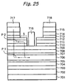
- FIG. 25 shows a seventeenth embodiment of the FET in accordance with the present invention. This embodiment executes the procedure of the eleventh embodiment by using the epitaxial layer of the seventh embodiment. As shown, gaps are formed at the sides of the gate electrode 716.
- a depletion layer tending to extend from the surface of the GaAs layer 712 toward the channel side stops in the GaAs layers 712, 711 and 710. This is successful to obstruct the rise of a conduction band at the surface side in the channel, so that a great amount of electrons can be stored in the above layer. Further, a current path is formed not only in the channel (P1, FIG. 25) but also in the gate buried layer (P2, FIG. 25), so that the sheet resistance is reduced in the exposed portion of the GaAs gate buried layer (S, FIG. 25).
- two-dimensional electron gas formed in the undoped GaAs layer 714 lowers the potential barrier of the Al 0.2 Ga 0.8 As layer 713 and thereby increases the probability that electrons pass through the potential barrier of the Al 0.2 Ga 0.8 As layer 713.
- the scattering by ionized impurities is suppressed and electron mobility is high in the layer 714. Consequently, the contact resistance from the cap layer 715 to the channel layer 706 is successfully reduced.
- an ON resistance as low as 1.3 ⁇ mm was achieved. This ON resistance is lower than the ON resistance of conventional FETs by 0.3 ⁇ mm. Also, a gate breakdown voltage of 15 V was achievable because of the gaps formed at the sides of the gate electrode 716.
- FIG. 26 shows an eighteenth embodiment of the FET in accordance with the present invention. This embodiment executes the process of eleventh embodiment by using the epitaxial layer of the eighth embodiment. As shown, gaps are formed at the sides of the gate electrode 816.
- the high concentration doping of the GaAs layer 811 stops the extension of a depletion layer from the surface of the GaAs layer 812 toward the channel side in the GaAs layers 812, 811 and 810. This is successful to obstruct the rise of a conduction band at the surface side in the channel right below the exposed GaAs layer, so that a great amount of electrons can be stored in the above layer. Further, a current path is formed not only in the channel (P1, FIG. 26) but also in the gate buried layer (P2, FIG. 26), so that the sheet resistance is reduced in the exposed portion of the GaAs gate buried layer (S FIG. 26).
- two-dimensional electron gas formed in the undoped GaAs layers 812 and 814 lowers the potential barrier and thereby increases the probability that electrons pass through the potential barrier of the Al 0.2 Ga 0.8 As layer 813.
- the scattering by ionized impurities is suppressed and electron mobility is high in the layers 812 and 814. Consequently, the contact resistance from the cap layer 815 to the channel layer 806 is successfully reduced.
- an ON resistance as low as 1.2 ⁇ mm was achieved. This ON resistance is lower than the ON resistance of conventional FETs by 0.4 ⁇ mm. Also, a gate breakdown voltage of 15 V was achievable because of the gaps formed at the sides of the gate electrode 816.
- FIG. 27 shows a nineteenth embodiment of the FET in accordance with the present invention. This embodiment executes the procedure of the eleventh embodiment by using the epitaxial wafer of the ninth embodiment. As shown, gaps are formed at the sides of the gate electrode 916.
- the high concentration doping of the GaAs layer 911 stops the extension of a depletion layer from the surface of the GaAs layer 912 toward the channel side in the GaAs layers 912, 911 and 910. This is successful to obstruct the rise of a conduction band at the surface side in the channel right below the exposed GaAs layer, so that a great amount of electrons can be stored in the above layer. Further, two-dimensional electron gas is formed in the GaAs layer 910. This, coupled with the fact that the GaAs layer 910 is undoped, reduces diffusion and therefore enhances mobility. A low resistance current path (P2, FIG. 27) is formed by the undoped GaAs layer 910 in addition to a current path (P1, FIG. 27) formed by the channel layer 906. Consequently, the sheet resistance is reduced in the portion where the GaAs gate buried layer 912 is exposed (S, FIG. 27).
- two-dimensional electron gas formed in the undoped GaAs layers 910 and 914 lowers the potential barrier and thereby increases the probability that electrons pass through the potential barrier of the Al 0.2 Ga 0.8 As layer 913 and a potential barrier formed by the Al 0.2 Ga 0.8 As layers 909, 908 and 907. Because electron mobility in the undoped GaAs layers 910 and 914 is high, the contact resistance from the cap layer 915 to the channel layer 906 is lowered.
- an ON resistance as low as 1.2 ⁇ mm was achieved. This ON resistance is lower than the ON resistance of conventional FETs by 0.4 ⁇ mm. Also, a gate breakdown voltage of 15 V was achieved because of the gaps formed at the sides of the gate electrode 916.
- FIG. 28 shows a twentieth embodiment of the FET in accordance with the present invention. This embodiment executes the process of the eleventh embodiment by using the epitaxial wafer of the tenth embodiment. As shown, gaps are formed at the sides of the gate electrode 1016.
- the high concentration doping of the GaAs layer 1011 stops the extension of a depletion layer from the surface of the GaAs layer 1012 toward the channel side in the GaAs layers 1012, 1011 and 1010. This is successful to obstruct the rise of a conduction band at the surface side in the channel right below the exposed GaAs layer 1012, so that a great amount of electrons can be stored in the above layer. Further, two-dimensional electron gas is formed in the GaAs layer 1010. This, coupled with the fact that the GaAs layer 1010 is undoped, reduces diffusion and therefore enhances mobility.
- a low resistance current path P2, FIG.
- two-dimensional electron gas formed in the undoped GaAs layers 1010, 1012 and 1014 lowers the potential barrier and thereby increases the probability that electrons pass through the potential barrier of the Al 0.2 Ga 0.8 As layer 1013 and a potential barrier formed by the Al 0.2 Ga 0.8 As layers 1009, 1008 and 1007. Because electron mobility in the undoped GaAs layers 1010, 1012 and 1014 is high, the contact resistance from the cap layer 1015 to the channel layer 1006 is lowered.
- an ON resistance as low as 1.1 ⁇ mm was achieved. This ON resistance is lower than the ON resistance of conventional FETs by 0.5 ⁇ mm. Also, a gate breakdown voltage of 15 V was achieved because of the gaps formed at the sides of the gate electrode 1016.
- a twenty-first embodiment of the FET in accordance with the present invention includes a semi-insulating GaAs substrate 2101.
- a 400 nm thick undoped GaAs buffer layer 2102 a 100 nm thick undoped Al 0.2 Ga 0.8 As buffer layer 2103, a 4 nm thick Al 0.2 Ga 0.8 As electron supply layer 2104 doped with 4 x 10 18 cm -3 of Si, a 2 nm thick undoped Al 0.2 Ga 0.8 As spacer layer 2105, a 15 nm thick undoped In 0.2 Ga 0.8 As channel layer 2106, a 2 nm thick undoped Al 0.2 Ga 0.8 As spacer layer 2107, a 9 nm thick Al 0.2 Ga 0.8 As electron supply layer 2108 doped with 4 x 10 18 cm -3 of Si, a 10 nm thick Al 0.2 Ga 0.8 As gate contact layer 2109 doped with 5 x 10 17 cm
- a mask formed with a wide recess pattern is formed on the wafer.
- the GaAs layer 2112 is selectively etched with the wide-recess stopper layer 2111 serving as a stop layer.
- dry etching using a mixture of chloride gas containing only chlorine as a halogen element and fluoride gas containing only fluorine, e.g., a BCl 3 and SF 6 mixture.
- the GaAs gate buried layer 2110 is selectively etched via a new mask formed with a gate recess pattern with the gate contact layer 2109 serving as a stopper layer. As a result, the undoped gate contact layer 2109 is exposed to the outside. At this instant, the buried layer 2110 is not overetched. A gate electrode 2113 is formed on the exposed gate contact layer 2109. This produces a structure in which no gaps are present at the sides of the gate electrode 2113.
- a source electrode 2114 and a drain electrode 2115 are formed by the evaporation lift-off and alloying (e.g. 400°C/1 min) of AuGe, serving as ohmic electrodes.
- the high concentration n-type impurities doped in the gate contact layer 2109 and wide-recess stopper layer 2111 increase the amount of electrons stored around the interface between the gate buried layer 2110 and cap layer 2112 and the gate contact layer 2109. This successfully reduces contact resistance from the cap layer 2112 to the channel layer 2106. Further, because the gate contact layer 2109 is not exposed to the outside, the sheet resistance increase of this portion is suppressed.
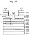
- FIG. 30 shows a twenty-second embodiment of the FET in accordance with the present invention.
- a semi-insulating GaAs substrate 2201 a 400 nm thick undoped GaAs buffer layer 2202, a 100 a thick undoped Al 0.2 Ga 0.8 As buffer layer 2203, a 4 nm thick Al 0.2 Ga 0.8 As electron supply layer 2204 doped with 4 x 10 18 cm -3 of Si, a 2 nm thick undoped Al 0.2 Ga 0.8 As spacer layer 2205, a 15 nm thick undoped In 0.2 Ga 0.8 As channel layer 2206, a 2 nm thick undoped Al 0.2 Ga 0.8 As spacer layer 2207, a 9 nm thick Al 0.2 Ga 0.8 As electron supply layer 2208 doped with 4 x 10 18 cm -3 of Si, a 10 nm thick Al 0.2 Ga 0.8 As gate contact layer 2209 doped with 5 x 10 17 cm -3 of Si, a 20 nm thick Ga
- a mask formed with a wide recess pattern is formed on the wafer.
- the GaAs layer 2214 is selectively etched with the wide-recess stopper layer 2213 serving as a stopper layer.
- dry etching using a mixture of chloride gas containing only chlorine as a halogen element and fluoride gas containing only fluorine, e.g., a BCl 3 and SF 6 mixture.
- the GaAs gate buried layers 2210, 2211 and 2212 are selectively etched via a new mask formed with a gate recess pattern with the gate contact layer 2209 serving as a stopper layer.
- the undoped gate contact layer 2209 is exposed to the outside.
- the gate buried layers 2210, 2211 and 2212 are not overetched.
- a gate electrode 2215 is formed on the exposed gate contact layer 2209. This produces a structure in which no gaps are present at the sides of the gate electrode 2215.
- a source electrode 2216 and a drain electrode 2217 are formed by the evaporation lift-off and alloying (e.g. 400°C/1 min) of AuGe, serving as ohmic electrodes.
- the high concentration n-type impurities doped in the gate contact layer 2209 and wide-recess stopper layer 2211 increase the amount of electrodes stored around the interface between the gate buried layer 2210 and cap layer 2214 and the gate contact layer 2209. This successfully reduces the contact resistance from the cap layer 2214 to the channel layer 2206. Further, the extension of a depletion layer from the surface of the GaAs layer 2212 toward the channel side is stopped in the GaAs layers 2212, 2211 and 2210. This is successful to obstruct the rise of a conduction band at the surface side in the channel and therefore to obviate exhaustion of electrons in the channel. Moreover, a current path is formed not only in the channel (P1, FIG.
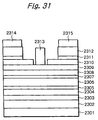
- FIG. 31 shows a twenty-third embodiment of the FET in accordance with the present invention. This embodiment executes the process of the eleventh embodiment by using the epitaxial wafer of the twenty-first embodiment. As shown, gaps are formed at the sides of the gate electrode 2313.
- the high concentration n-type impurities doped in the gate contact layer 2309 and wide-recess stopper layer 2311 increase the amount of electrodes stored around the interface between the gate buried layer 2310 and cap layer 2312 and the gate contact layer 2309. This successfully reduces the contact resistance from the cap layer 2312 to the channel layer 2306. Further, because the gate contact layer 2309 is not exposed to the outside, the sheet resistance in this portion sparingly increases.
- an ON resistance as low as 1.4 ⁇ mm was achieved. This ON resistance is lower than the ON resistance of conventional FETs by 0.2 ⁇ mm. Also, a gate breakdown voltage of 15 V was achieved because of the gaps formed at the sides of the gate electrode 2313.
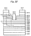
- FIG. 32 shows a twenty-fourth embodiment of the FET in accordance with the present invention. This embodiment executes the process of the eleventh embodiment by using the epitaxial wafer of the twenty-second embodiment. As shown, gaps are formed at the sides of the gate electrode 2413.
- the high concentration n-type impurities doped in the gate contact layer 2409 and wide-recess stopper layer 241 increase the amount of electrodes stored around the interface between the gate buried layer 240 and cap layer 2412 and the gate contact layer 2409. This successfully reduces the contact resistance from the cap layer to the channel layer 2406. Further, the extension of a depletion layer from the surface of the GaAs layer 2412 toward the channel side is stopped in the GaAs layers 2412, 2411 and 2410. This is successful to obstruct the rise of a conduction band at the surface side in the channel and therefore to obviate exhaustion of electrons in the channel. Moreover, a current path is formed not only in the channel (P1, FIG. 32) but also in the gate buried layer (P2, FIG. 32), so that the sheet resistance is reduced in the exposed GaAs gate buried layer portion (S, FIG. 32).
- an ON resistance as low as 1.3 ⁇ mm was achieved. This ON resistance is lower than the ON resistance of conventional FETs by 0.3 ⁇ mm. Also, a gate breakdown voltage of 15 V was achieved because of the gaps formed at the side of the gate electrode 2413.
- each includes an InGaAs channel layer having an In composition of about 0.2 customarily used on a GaAs substrate.
- Such an InGaAs channel layer may be replaced with a GaAs channel layer, if desired.
- the present invention is practicable with a single dope, single hetero structure in place of the double dope, double hetero structure positioning the AlGaAs electron supply layer on the top and bottom of the channel layer.
- the present invention may even be implemented as a hetero junction FET fabricated on InP, i.e., including an In 0.5 Al 0.5 As layer in place of the AlGaAs layer and including an In 0.5 Ga 0.5 As layer in place of the In 0.2 Ga 0.8 As layer.
- a tartaric etchant in place of the dry etching scheme mentioned in relation to the illustrative embodiments.
- the present invention provides a hetero junction FET capable of achieving an ON resistance noticeably lower than the conventional ON resistance.
Landscapes
- Junction Field-Effect Transistors (AREA)
Applications Claiming Priority (2)
| Application Number | Priority Date | Filing Date | Title |
|---|---|---|---|
| JP5456998 | 1998-03-06 | ||
| JP10054569A JP3107031B2 (ja) | 1998-03-06 | 1998-03-06 | 電界効果トランジスタ |
Publications (2)
| Publication Number | Publication Date |
|---|---|
| EP0940855A2 true EP0940855A2 (de) | 1999-09-08 |
| EP0940855A3 EP0940855A3 (de) | 1999-09-22 |
Family
ID=12974334
Family Applications (1)
| Application Number | Title | Priority Date | Filing Date |
|---|---|---|---|
| EP99104470A Withdrawn EP0940855A3 (de) | 1998-03-06 | 1999-03-05 | Feldeffekttransistor mit III-V Halbleiterheteroübergang |
Country Status (5)
| Country | Link |
|---|---|
| US (2) | US20020074563A1 (de) |
| EP (1) | EP0940855A3 (de) |
| JP (1) | JP3107031B2 (de) |
| KR (1) | KR100278463B1 (de) |
| CN (1) | CN1160796C (de) |
Cited By (3)
| Publication number | Priority date | Publication date | Assignee | Title |
|---|---|---|---|---|
| EP1424734A3 (de) * | 2002-11-26 | 2005-03-02 | NEC Compound Semiconductor Devices, Ltd. | Heteroübergang-Feldeffekt-Halbleiteranordnung mit hoher Anschaltspannung und niedriegem Anschaltwiderstand und Verfahren zur Herstellung |
| RU2257642C1 (ru) * | 2004-07-13 | 2005-07-27 | Государственное образовательное учреждение высшего профессионального образования "Таганрогский государственный радиотехнический университет" (ТРТУ) | Интегральный полевой транзистор с размерным квантованием энергии |
| CN110998859A (zh) * | 2017-07-06 | 2020-04-10 | 特励达科学与成像有限责任公司 | 具有掩埋栅极结构的fet |
Families Citing this family (15)
| Publication number | Priority date | Publication date | Assignee | Title |
|---|---|---|---|---|
| JP2002217212A (ja) * | 2001-01-19 | 2002-08-02 | Murata Mfg Co Ltd | ヘテロ接合電界効果トランジスタ |
| JP2003174039A (ja) | 2001-09-27 | 2003-06-20 | Murata Mfg Co Ltd | ヘテロ接合電界効果トランジスタ |
| JP4064800B2 (ja) * | 2002-12-10 | 2008-03-19 | 株式会社東芝 | ヘテロ接合型化合物半導体電界効果トランジスタ及びその製造方法 |
| US20050104087A1 (en) * | 2003-11-19 | 2005-05-19 | Lan Ellen Y. | InGaP pHEMT device for power amplifier operation over wide temperature range |
| JP2005340549A (ja) * | 2004-05-28 | 2005-12-08 | Sanyo Electric Co Ltd | 半導体装置およびその製造方法 |
| CN100342547C (zh) * | 2004-06-08 | 2007-10-10 | 中国科学院半导体研究所 | 高击穿电压的高电子迁移率晶体管 |
| JP2007027594A (ja) * | 2005-07-21 | 2007-02-01 | Nec Electronics Corp | 電界効果トランジスタ |
| JP2007103425A (ja) * | 2005-09-30 | 2007-04-19 | Oki Electric Ind Co Ltd | 化合物半導体からなる電界効果トランジスタ |
| JP2007311684A (ja) | 2006-05-22 | 2007-11-29 | Mitsubishi Electric Corp | 電界効果型トランジスタ |
| US8115235B2 (en) * | 2009-02-20 | 2012-02-14 | Intel Corporation | Modulation-doped halo in quantum well field-effect transistors, apparatus made therewith, and methods of using same |
| JP5504427B2 (ja) * | 2009-03-16 | 2014-05-28 | 旭化成エレクトロニクス株式会社 | 電界効果トランジスタ |
| US8617976B2 (en) * | 2009-06-01 | 2013-12-31 | Taiwan Semiconductor Manufacturing Company, Ltd. | Source/drain re-growth for manufacturing III-V based transistors |
| US8193523B2 (en) | 2009-12-30 | 2012-06-05 | Intel Corporation | Germanium-based quantum well devices |
| JP5857390B2 (ja) * | 2012-03-30 | 2016-02-10 | 住友電工デバイス・イノベーション株式会社 | 半導体装置 |
| CN118553764B (zh) * | 2024-07-26 | 2024-11-12 | 厦门市三安集成电路有限公司 | 一种半导体器件 |
Family Cites Families (11)
| Publication number | Priority date | Publication date | Assignee | Title |
|---|---|---|---|---|
| EP0143656B1 (de) * | 1983-11-29 | 1989-02-22 | Fujitsu Limited | Halbleiteranordnung mit Verbindungshalbleiter und Verfahren zu dessen Herstellung |
| JPS63221683A (ja) | 1987-03-10 | 1988-09-14 | Nec Corp | 電界効果トランジスタ |
| JP2626213B2 (ja) * | 1990-08-23 | 1997-07-02 | 日本電気株式会社 | 電界効果トランジスタ |
| JPH04186849A (ja) | 1990-11-21 | 1992-07-03 | Hitachi Ltd | ヘテロ接合電界効果トランジスタ |
| JPH0766984B2 (ja) | 1992-02-13 | 1995-07-19 | インターナショナル・ビジネス・マシーンズ・コーポレイション | ヘテロ超格子pn接合 |
| FR2689683B1 (fr) * | 1992-04-07 | 1994-05-20 | Thomson Composants Microondes | Dispositif semiconducteur a transistors complementaires. |
| JP3232519B2 (ja) | 1993-08-30 | 2001-11-26 | 日本電信電話株式会社 | オーミックヘテロ接合構造 |
| JPH07111327A (ja) | 1993-10-13 | 1995-04-25 | Nippondenso Co Ltd | ヘテロ接合型電界効果トランジスタ |
| JP2581452B2 (ja) | 1994-06-06 | 1997-02-12 | 日本電気株式会社 | 電界効果トランジスタ |
| JPH1056168A (ja) | 1996-08-08 | 1998-02-24 | Mitsubishi Electric Corp | 電界効果トランジスタ |
| JP3147009B2 (ja) * | 1996-10-30 | 2001-03-19 | 日本電気株式会社 | 電界効果トランジスタ及びその製造方法 |
-
1998
- 1998-03-06 JP JP10054569A patent/JP3107031B2/ja not_active Expired - Fee Related
-
1999
- 1999-03-05 EP EP99104470A patent/EP0940855A3/de not_active Withdrawn
- 1999-03-05 CN CNB991034473A patent/CN1160796C/zh not_active Expired - Fee Related
- 1999-03-06 KR KR1019990007474A patent/KR100278463B1/ko not_active Expired - Fee Related
- 1999-03-08 US US09/263,838 patent/US20020074563A1/en not_active Abandoned
-
2001
- 2001-10-30 US US10/021,540 patent/US6624440B2/en not_active Expired - Fee Related
Cited By (5)
| Publication number | Priority date | Publication date | Assignee | Title |
|---|---|---|---|---|
| EP1424734A3 (de) * | 2002-11-26 | 2005-03-02 | NEC Compound Semiconductor Devices, Ltd. | Heteroübergang-Feldeffekt-Halbleiteranordnung mit hoher Anschaltspannung und niedriegem Anschaltwiderstand und Verfahren zur Herstellung |
| US7071499B2 (en) | 2002-11-26 | 2006-07-04 | Nec Electronics Corporation | Heterojunction field effect type semiconductor device having high gate turn-on voltage and low on-resistance and its manufacturing method |
| RU2257642C1 (ru) * | 2004-07-13 | 2005-07-27 | Государственное образовательное учреждение высшего профессионального образования "Таганрогский государственный радиотехнический университет" (ТРТУ) | Интегральный полевой транзистор с размерным квантованием энергии |
| CN110998859A (zh) * | 2017-07-06 | 2020-04-10 | 特励达科学与成像有限责任公司 | 具有掩埋栅极结构的fet |
| CN110998859B (zh) * | 2017-07-06 | 2024-02-09 | 特励达科学与成像有限责任公司 | 具有掩埋栅极结构的fet |
Also Published As
| Publication number | Publication date |
|---|---|
| US20020053682A1 (en) | 2002-05-09 |
| KR19990077669A (ko) | 1999-10-25 |
| JP3107031B2 (ja) | 2000-11-06 |
| EP0940855A3 (de) | 1999-09-22 |
| CN1160796C (zh) | 2004-08-04 |
| KR100278463B1 (ko) | 2001-01-15 |
| US20020074563A1 (en) | 2002-06-20 |
| JPH11251575A (ja) | 1999-09-17 |
| US6624440B2 (en) | 2003-09-23 |
| CN1236998A (zh) | 1999-12-01 |
Similar Documents
| Publication | Publication Date | Title |
|---|---|---|
| US6624440B2 (en) | Field effect transistor | |
| EP0551110B1 (de) | Verbindungshalbleiterbauelemente | |
| US20010019131A1 (en) | Field effect transistor and manufacturing method thereof | |
| JPH08162647A (ja) | 半導体装置 | |
| JP2001144110A (ja) | 半導体装置及びその製造方法 | |
| US6426523B1 (en) | Heterojunction field effect transistor | |
| JPH0815213B2 (ja) | 電界効果トランジスタ | |
| US12154982B2 (en) | Gallium nitride transistor | |
| US20040155261A1 (en) | Semiconductor device and manufacturing method thereof | |
| JPH07142706A (ja) | ヘテロ接合半導体装置の製造方法およびヘテロ接合半導体装置 | |
| EP1083608B1 (de) | Feldeffekt-Halbleiteranordnung | |
| JPS62256477A (ja) | 半導体装置 | |
| KR940010557B1 (ko) | 반도체장치 | |
| JP3077599B2 (ja) | 電界効果トランジスタ | |
| JPH05175494A (ja) | トンネルトランジスタ | |
| JP2500459B2 (ja) | ヘテロ接合電界効果トランジスタ | |
| JP3112075B2 (ja) | 電界効果トランジスタ及びその製造方法 | |
| JP3107002B2 (ja) | 電界効果トランジスタとその製造方法 | |
| JPH06252176A (ja) | 高電子移動度トランジスタ | |
| JP2658513B2 (ja) | 電界効果トランジスタ | |
| JPS5891681A (ja) | 電界効果型トランジスタ | |
| JP3141841B2 (ja) | ヘテロ接合電界効果トランジスタ | |
| JPH05315368A (ja) | 電界効果トランジスタ | |
| JPH05291306A (ja) | ヘテロ接合型電界効果トランジスタの素子間分離方法 | |
| JPH0653253A (ja) | 電界効果トランジスタ |
Legal Events
| Date | Code | Title | Description |
|---|---|---|---|
| PUAI | Public reference made under article 153(3) epc to a published international application that has entered the european phase |
Free format text: ORIGINAL CODE: 0009012 |
|
| PUAL | Search report despatched |
Free format text: ORIGINAL CODE: 0009013 |
|
| AK | Designated contracting states |
Kind code of ref document: A2 Designated state(s): DE FR GB |
|
| AX | Request for extension of the european patent |
Free format text: AL;LT;LV;MK;RO;SI |
|
| AK | Designated contracting states |
Kind code of ref document: A3 Designated state(s): AT BE CH CY DE DK ES FI FR GB GR IE IT LI LU MC NL PT SE |
|
| AX | Request for extension of the european patent |
Free format text: AL;LT;LV;MK;RO;SI |
|
| RTI1 | Title (correction) |
Free format text: III-V SEMICONDUCTOR HETEROJUNCTION FIELD EFFECT TRANSISTOR |
|
| RTI1 | Title (correction) |
Free format text: III-V SEMICONDUCTOR HETEROJUNCTION FIELD EFFECT TRANSISTOR |
|
| 17P | Request for examination filed |
Effective date: 19990813 |
|
| AKX | Designation fees paid |
Free format text: DE FR GB |
|
| 17Q | First examination report despatched |
Effective date: 20030718 |
|
| GRAP | Despatch of communication of intention to grant a patent |
Free format text: ORIGINAL CODE: EPIDOSNIGR1 |
|
| STAA | Information on the status of an ep patent application or granted ep patent |
Free format text: STATUS: THE APPLICATION HAS BEEN WITHDRAWN |
|
| 18W | Application withdrawn |
Effective date: 20041123 |