EP0959051A1 - Procede d'usinage au laser pour substrat de verre, dispositif optique du type a diffraction fabrique par ce procede d'usinage, et procede de fabrication de ce dispositif optique - Google Patents
Procede d'usinage au laser pour substrat de verre, dispositif optique du type a diffraction fabrique par ce procede d'usinage, et procede de fabrication de ce dispositif optique Download PDFInfo
- Publication number
- EP0959051A1 EP0959051A1 EP97934765A EP97934765A EP0959051A1 EP 0959051 A1 EP0959051 A1 EP 0959051A1 EP 97934765 A EP97934765 A EP 97934765A EP 97934765 A EP97934765 A EP 97934765A EP 0959051 A1 EP0959051 A1 EP 0959051A1
- Authority
- EP
- European Patent Office
- Prior art keywords
- laser beam
- thin film
- glass substrate
- laser
- intensity distribution
- Prior art date
- Legal status (The legal status is an assumption and is not a legal conclusion. Google has not performed a legal analysis and makes no representation as to the accuracy of the status listed.)
- Withdrawn
Links
Images


Classifications
-
- C—CHEMISTRY; METALLURGY
- C03—GLASS; MINERAL OR SLAG WOOL
- C03C—CHEMICAL COMPOSITION OF GLASSES, GLAZES OR VITREOUS ENAMELS; SURFACE TREATMENT OF GLASS; SURFACE TREATMENT OF FIBRES OR FILAMENTS MADE FROM GLASS, MINERALS OR SLAGS; JOINING GLASS TO GLASS OR OTHER MATERIALS
- C03C23/00—Other surface treatment of glass not in the form of fibres or filaments
- C03C23/0005—Other surface treatment of glass not in the form of fibres or filaments by irradiation
- C03C23/0025—Other surface treatment of glass not in the form of fibres or filaments by irradiation by a laser beam
-
- B—PERFORMING OPERATIONS; TRANSPORTING
- B23—MACHINE TOOLS; METAL-WORKING NOT OTHERWISE PROVIDED FOR
- B23K—SOLDERING OR UNSOLDERING; WELDING; CLADDING OR PLATING BY SOLDERING OR WELDING; CUTTING BY APPLYING HEAT LOCALLY, e.g. FLAME CUTTING; WORKING BY LASER BEAM
- B23K26/00—Working by laser beam, e.g. welding, cutting or boring
- B23K26/02—Positioning or observing the workpiece, e.g. with respect to the point of impact; Aligning, aiming or focusing the laser beam
- B23K26/06—Shaping the laser beam, e.g. by masks or multi-focusing
- B23K26/064—Shaping the laser beam, e.g. by masks or multi-focusing by means of optical elements, e.g. lenses, mirrors or prisms
- B23K26/066—Shaping the laser beam, e.g. by masks or multi-focusing by means of optical elements, e.g. lenses, mirrors or prisms by using masks
-
- C—CHEMISTRY; METALLURGY
- C03—GLASS; MINERAL OR SLAG WOOL
- C03C—CHEMICAL COMPOSITION OF GLASSES, GLAZES OR VITREOUS ENAMELS; SURFACE TREATMENT OF GLASS; SURFACE TREATMENT OF FIBRES OR FILAMENTS MADE FROM GLASS, MINERALS OR SLAGS; JOINING GLASS TO GLASS OR OTHER MATERIALS
- C03C17/00—Surface treatment of glass, not in the form of fibres or filaments, by coating
- C03C17/22—Surface treatment of glass, not in the form of fibres or filaments, by coating with other inorganic material
- C03C17/23—Oxides
-
- C—CHEMISTRY; METALLURGY
- C03—GLASS; MINERAL OR SLAG WOOL
- C03C—CHEMICAL COMPOSITION OF GLASSES, GLAZES OR VITREOUS ENAMELS; SURFACE TREATMENT OF GLASS; SURFACE TREATMENT OF FIBRES OR FILAMENTS MADE FROM GLASS, MINERALS OR SLAGS; JOINING GLASS TO GLASS OR OTHER MATERIALS
- C03C17/00—Surface treatment of glass, not in the form of fibres or filaments, by coating
- C03C17/34—Surface treatment of glass, not in the form of fibres or filaments, by coating with at least two coatings having different compositions
- C03C17/3411—Surface treatment of glass, not in the form of fibres or filaments, by coating with at least two coatings having different compositions with at least two coatings of inorganic materials
- C03C17/3417—Surface treatment of glass, not in the form of fibres or filaments, by coating with at least two coatings having different compositions with at least two coatings of inorganic materials all coatings being oxide coatings
-
- C—CHEMISTRY; METALLURGY
- C03—GLASS; MINERAL OR SLAG WOOL
- C03C—CHEMICAL COMPOSITION OF GLASSES, GLAZES OR VITREOUS ENAMELS; SURFACE TREATMENT OF GLASS; SURFACE TREATMENT OF FIBRES OR FILAMENTS MADE FROM GLASS, MINERALS OR SLAGS; JOINING GLASS TO GLASS OR OTHER MATERIALS
- C03C17/00—Surface treatment of glass, not in the form of fibres or filaments, by coating
- C03C17/34—Surface treatment of glass, not in the form of fibres or filaments, by coating with at least two coatings having different compositions
- C03C17/3411—Surface treatment of glass, not in the form of fibres or filaments, by coating with at least two coatings having different compositions with at least two coatings of inorganic materials
- C03C17/3429—Surface treatment of glass, not in the form of fibres or filaments, by coating with at least two coatings having different compositions with at least two coatings of inorganic materials at least one of the coatings being a non-oxide coating
- C03C17/3447—Surface treatment of glass, not in the form of fibres or filaments, by coating with at least two coatings having different compositions with at least two coatings of inorganic materials at least one of the coatings being a non-oxide coating comprising a halide
- C03C17/3452—Surface treatment of glass, not in the form of fibres or filaments, by coating with at least two coatings having different compositions with at least two coatings of inorganic materials at least one of the coatings being a non-oxide coating comprising a halide comprising a fluoride
-
- C—CHEMISTRY; METALLURGY
- C03—GLASS; MINERAL OR SLAG WOOL
- C03C—CHEMICAL COMPOSITION OF GLASSES, GLAZES OR VITREOUS ENAMELS; SURFACE TREATMENT OF GLASS; SURFACE TREATMENT OF FIBRES OR FILAMENTS MADE FROM GLASS, MINERALS OR SLAGS; JOINING GLASS TO GLASS OR OTHER MATERIALS
- C03C2217/00—Coatings on glass
- C03C2217/20—Materials for coating a single layer on glass
- C03C2217/21—Oxides
- C03C2217/212—TiO2
-
- C—CHEMISTRY; METALLURGY
- C03—GLASS; MINERAL OR SLAG WOOL
- C03C—CHEMICAL COMPOSITION OF GLASSES, GLAZES OR VITREOUS ENAMELS; SURFACE TREATMENT OF GLASS; SURFACE TREATMENT OF FIBRES OR FILAMENTS MADE FROM GLASS, MINERALS OR SLAGS; JOINING GLASS TO GLASS OR OTHER MATERIALS
- C03C2217/00—Coatings on glass
- C03C2217/20—Materials for coating a single layer on glass
- C03C2217/21—Oxides
- C03C2217/213—SiO2
-
- C—CHEMISTRY; METALLURGY
- C03—GLASS; MINERAL OR SLAG WOOL
- C03C—CHEMICAL COMPOSITION OF GLASSES, GLAZES OR VITREOUS ENAMELS; SURFACE TREATMENT OF GLASS; SURFACE TREATMENT OF FIBRES OR FILAMENTS MADE FROM GLASS, MINERALS OR SLAGS; JOINING GLASS TO GLASS OR OTHER MATERIALS
- C03C2218/00—Methods for coating glass
- C03C2218/30—Aspects of methods for coating glass not covered above
- C03C2218/32—After-treatment
- C03C2218/328—Partly or completely removing a coating
-
- Y—GENERAL TAGGING OF NEW TECHNOLOGICAL DEVELOPMENTS; GENERAL TAGGING OF CROSS-SECTIONAL TECHNOLOGIES SPANNING OVER SEVERAL SECTIONS OF THE IPC; TECHNICAL SUBJECTS COVERED BY FORMER USPC CROSS-REFERENCE ART COLLECTIONS [XRACs] AND DIGESTS
- Y10—TECHNICAL SUBJECTS COVERED BY FORMER USPC
- Y10T—TECHNICAL SUBJECTS COVERED BY FORMER US CLASSIFICATION
- Y10T428/00—Stock material or miscellaneous articles
- Y10T428/24—Structurally defined web or sheet [e.g., overall dimension, etc.]
- Y10T428/24273—Structurally defined web or sheet [e.g., overall dimension, etc.] including aperture
-
- Y—GENERAL TAGGING OF NEW TECHNOLOGICAL DEVELOPMENTS; GENERAL TAGGING OF CROSS-SECTIONAL TECHNOLOGIES SPANNING OVER SEVERAL SECTIONS OF THE IPC; TECHNICAL SUBJECTS COVERED BY FORMER USPC CROSS-REFERENCE ART COLLECTIONS [XRACs] AND DIGESTS
- Y10—TECHNICAL SUBJECTS COVERED BY FORMER USPC
- Y10T—TECHNICAL SUBJECTS COVERED BY FORMER US CLASSIFICATION
- Y10T428/00—Stock material or miscellaneous articles
- Y10T428/24—Structurally defined web or sheet [e.g., overall dimension, etc.]
- Y10T428/24479—Structurally defined web or sheet [e.g., overall dimension, etc.] including variation in thickness
- Y10T428/2457—Parallel ribs and/or grooves
Definitions
- the present invention relates to a laser processing method for processing a micro convexo-concave structure on a surface of a glass substrate and an optical diffraction element obtained by the laser processing method, and to a method for manufacturing an optical element including a diffraction grating which is used as a polarized light beam splitter, a coupling grating or the like, a diffraction type optical element which is used for a hologram, or an optical element such as a photonic crystal which is used as a birefringent plate, a light beam scatter plate or the like.
- a glass plate has superior characteristics with respect to flatness, processing accuracy, weather resistance, heat resistance, etc. Therefore, there are already known devices such as a diffraction grating for use in optical communication and so on, or a micro lens for installation in a display device, which are formed by performing micro processing on a surface of a glass substrate.
- a wet etching (chemical etching) method by using an etchant including hydrofluoric acid, etc.
- a dry etching (physical etching) method by using a reactive ion etching, etc.
- an element for dividing wavelength such as a diffraction grating, etc., which is available commercially at a relatively cheap price, is industrially produced by a method of obtaining an original negative plate by cutting a metal plate of aluminum or the like with a diamond blade (so called "a ruling engine") and transferring upon an epoxy resin on the basis thereof.
- a laser beam has strong energy so that the temperature of an irradiated surface of any arbitrary material increases resulting in ablation or evaporation of the irradiated portion thereof. Therefore, conventionally, a laser beam has been utilized in various processings or machining methods. In particular, the method of using a laser has been adapted to micro processing or machining because the laser beam can be easily focused onto a very fine spot.
- a wave guide (a thin layer or film) having an index of refraction higher than air and that of the material to be processed is provided on the material to be processed, such as the metal plate or the like, and the laser beam is radiated onto the wave guide, thereby forming micro convexo-concave patterns in the wave guide by interference between the light beams transmitted in the wave guide and the radiated light beam, and providing a rainbow color developing function on the surface of the material to be processed.
- the thin film is formed on the surface of the substrate, thereby achieving a micro processing or machining thereon by absorbing the laser beam energy into the thin film to cause the ablation thereof.
- none of them takes into any consideration at all the energy of the laser beam.
- a laser beam having an intensity higher than a certain level of energy must be irradiated to cause the ablation and so on, not only is the micro convexo-concave structure formed on the thin film, but also the substrate itself is processed or affected by the laser, in a case where the thin film is formed on the surface of the substrate.
- the energy of the laser beam which reaches the substrate through the thin film is greater than a certain energy (threshold) that is enough to cause ablation on the substrate.
- micro processing on the substrate which is different in physical property from the thin film, is being carried out at the same time, it cannot be used as an optical element, such as the diffraction grating, etc., for which is required a certain level of accuracy thereof.
- the thin film comprises organic macromolecules.
- a diffraction grating in which periodic convexo-concave structures are formed on a dielectric multiple film layer in one direction has superior characteristics as a polarized light beam splitter (Rong-Chung et al., OPTICS LETTERS Vol. 21, No. 10, p761, 1996).
- a diffraction grating in which periodic convexo-concave structures are formed on a dielectric multiple film layer in two directions has been proposed as a photonic crystal of three dimension (E. Yablonovitch, Journal of the Optical Society of America B Vol. 10, No. 2, p283, 1993).
- a dielectric multiple film layer itself has been widely used in various technical fields as a mirror, etc., and also various techniques have been already established as the method for manufacturing thereof, including an electron beam evaporation method, a heating evaporation method and a sputtering method.
- a diffraction grating in which periodic convexo-concave structures are formed on a dielectric multiple film layer, can be produced by adopting the patterning technology for producing VLSI on a dielectric multiple film layer.
- a laser processing method to a glass substrate and an optical diffraction element obtained thereby with respect to the first and the second invention of the present application comprising the steps of: forming a thin film of a material showing superior absorption characteristics of a laser beam to that of the glass substrate, on a surface of which said thin film is formed; radiating the laser beam having an intensity distribution onto said thin film; and removing the thin film depending on the intensity distribution of the laser beam by fusion, evaporation or ablation which occurs by making said thin film absorb energy from the laser beam radiated thereon, wherein said thin film is made of inorganic materials, and a thickness or an absorption index of said thin film with respect to an intensity of the laser beam is set at a value less than a threshold value that is enough for the laser beam to reach a surface of said glass substrate penetrating through said thin film to cause the fusion, evaporation or ablation.
- the thin film there is appropriate a single layer or a plurality of layers of one or any combination of a glass of a metal oxide, a metal nitride, a metal carbide, a semiconductor, and silicon dioxide (SiO 2 ), a fluoride glass, and a chalcogenide glass.
- various methods can be applied thereto, including a sol-gel method, a sputtering method, a vacuum deposition method, and liquid-phase epitaxy method, and so on.
- Energy loss of the laser beam which occurs when it passes through the thin film, can be controlled by controlling a thickness of the thin film and an absorption index. However, in a case where it is necessary to keep a certain thickness, it may be controlled by varying (mainly) the absorption index for the laser beam.
- a method of controlling the absorption index there are a method of intensively introducing a shift in a ratio of quantum theory, such as of defective oxygen, a method of introducing a defect, a method of doping an ion showing high absorption with respect to the wavelength used, a method of mixing amicrons or ultra fine particles, a method of mixing a pigment, a method of mixing an organic pigment, etc.
- an optical diffraction element for use as a diffraction grating or a hologram installed in an optical coupler, a polariscope, a wave divider, a wavelength filter, a reflector, a mode transducer, etc., by using a laser beam having a periodic or regulative distribution in optical intensity.
- the thickness of the thin film becomes automatically to be equal to the thickness of the convexo-concave structure, by developing the ablation until the glass substrate appears at the bottom of the concave portion of the thin film.
- a laser beam having such a periodic optical intensity distribution can be obtained by a phase mask, or by interference between the laser beams, and thereby the configuration of a cross-section of the periodic convexo-concave pattern formed on the surface of the glass substrate can be controlled by the pulse energy of the laser beam.
- a laser beam having such a regulative optical intensity distribution can be obtained by using a net shaped mask, and so on.
- a method for manufacturing an optical element with respect to the third invention of the present application comprises the steps of: forming a dielectric multiple film layer, which comprises plural kinds of layers having different permittivities on the surface of a substrate; irradiating a laser beam having an intensity distribution onto said dielectric multiple film layer; and removing a portion of the dielectric multiple film layer depending on the intensity distribution of the laser beam by fusion, evaporation or ablation which occurs by making said dielectric multiple film layer absorb energy from the laser beam radiated thereon, so as to leave the other portions as the periodically arranged dielectric convex portions having a grating constant corresponding to the wavelength of the beam.
- the material forming said dielectric multiple film layer has a threshold value to cause the fusion, evaporation or ablation with respect to the laser beam that is lower than that of the substrate, and that it has a large adhesion in the film thereof.
- silicon oxide, titanium oxide, cerium oxide, germanium oxide, magnesium fluoride, calcium fluoride, tantalum oxide, etc. are appropriate.
- each layer of the multiple film layer can be formed as a glass (amorphous), in a single crystal or in a polycrystal.
- such laser beam can be obtained either through a phase mask or through an interference between two laser beams.
- such laser beam can be obtained through an interference among at least three laser beams.
- an excimer laser such as KrF, an Nd-YAG laser, a Ti:Al 2 O 3 laser and the high harmonics thereof, or a pigment laser
- a laser beam having a lower reflectivity with respect to the dielectric multiple film layer to be processed should be used.
- an SiO 2 thin layer or film in which colloidal Ag is dispersed.
- a method for forming there is used a sputtering method, in which an SiO 2 target and a chip of silver metal are positioned on a target and are sputtered at the same time. The sputtering condition is set as below for growing a film.
- a quartz target which is positioned below and which has a size of 5 inches X 20 inches, on which thirty two (32) disc-shaped chips of silver (having diameters of about 4 mm) are positioned in dispersed locations.
- the thin film obtained is a clear film which is brown colored, and has a flat surface and strong adhesion.
- the film grows to be 315 nm in thickness with 5 minutes of film growing time.
- a concentration of silver in the film which is measured by XPS (X-ray photoelectron spectroscopy) is 0.94 atom%.
- a peak of absorption is in the vicinity of 390 nm. It can be thought that this is caused by plasmon absorption by amicrons or ultra fine particles of silver (colloid) and that the amicrons or ultra fine particles of silver are produced in the glass during the growing of the film.
- a micro processing or machining is carried out by conducting an ablation on the thin film upon the surface of the glass, by an optical system shown in Fig. 1.
- a single laser beam is divided into two laser beams and then they are again focused on the thin film of the glass, thereby obtaining a periodically changing pattern of intensity by the interference therebetween.
- the laser which is used is an Nd:YAG laser having a pulse width of 10 ns, a repetitive frequency of 10 Hz, and the wavelength used is a 3rd high harmonic of 355 nm.
- the irradiation energy of the laser beam before division into two beams is about 110 mJ/Pulse.
- the laser beam after being divided by a 50% beam splitter and passing through the quartz lens, is irradiated onto the surface of a sample, and the two divided laser beams are combined to produce the interference, thereby forming the periodic distribution condition of the optical intensity.
- An angle defined between the laser beams is about 10 degrees.
- the diameter of the laser beam on the sample is 2 mm, and the energy density thereof is 4.14 J/cm 2 Pulse.
- the energy is set at a value a little bit higher than that of the energy sufficient to cause the ablation on the thin film, which is previously determined.
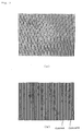
- Fig. 2(a) is a photomicrograph taken by an optical microscope at 1,000X magnification
- Fig. 2(b) is a drawing produced on the basis of the same photo
- Fig. 3(a) is a photomicrograph taken by a scanning type microscope at 3,500X magnification
- Fig. 3(b) is a drawing produced on the basis of the same photo. From those drawings, it can be ascertained that a periodic convexo-concave pattern of about 1 ⁇ m is formed on the film.
- an absorption coefficient of the thin film is 46,212 cm -1 at 355 nm.
- the absorption coefficient of the soda-lime glass substrate is 0.3081 cm -1 .
- the energy reaching the substrate, which is calculated by the absorption coefficient and the thickness of the thin film, is 0.95 J/cm 2 Pulse.
- a threshold value of the ablation of the glass is experimentally obtained. Namely, while increasing the irradiation energy, the energy at the time when the ablation occurs is recorded. An area of a mark or trace of the ablation is necessary for calculation of the power density, however, it is impossible to measure it correctly because of hard cracks appearing around the irradiation trace. Obtained from roughly estimating the area from it, the power density is found to be at least 8 to 10 J/cm 2 Pulse by the laser of the present embodiment. Accordingly, it can be thought that since the energy reaching the substrate is less than the threshold value necessary for the ablation of the substrate, the ablation occurs preferably on the thin film, thereby obtaining a fine processing.
- the ablation by using the interfered light is carried out on the glass attached with the thin film in the same manner as in Embodiment 1.
- the periodic pattern is formed on the film surface, and it functions as the diffraction grating. Every one of the thin films, as is apparent from the chart, has an absorption coefficient higher than that of the substrate, and also the laser energy reaching the substrate is lower than the threshold value for causing the ablation on the substrate.
- an SiO 2 thin film in which colloidal Ag is dispersed is formed. This is achieved by introducing those samples into the same chamber with Embodiments 4 and 5 at the same time, for the purpose of obtaining completely identical film characteristics.
- the substrate is made of a material having an ablation threshold value (3.5 J/cm 2 Pulse) which is lower than that of the substrate of Examples 1 through 5 (see the chart).
- a substrate (glass matrix) in which are dispersed amicrons or ultra fine particles of CdS or CdSe is widely used as a sharp cut filter.
- the ablation is carried out on the manufactured glass substrate with the thin film attached under the same conditions of Embodiment 1.
- the threshold value for processing the glass substrate is 3.5 J/cm 2 with respect to the wavelength of 355 nm, and its absorption coefficient is 377 cm -1 .
- the absorption coefficient of the film in Comparison 2 is 6490 cm -1 , and is higher than that of the substrate.
- the energy reaching the substrate penetrating through the thin film is 3.4 J/cm 2 which is somewhat lower than the ablation threshold value of the substrate.
- the absorption coefficient of the film is 2235 cm -1 , being higher than that of the substrate, i.e., 377 cm -1 , however, the energy reaching the substrate comes up to 3.9 J/cm 2 Pulse of the ablation threshold value of the substrate. Accordingly, it can be thought that this point is one reason for losing the possibility of effective processing.
- a diffraction grating is manufactured on the same sample used in Embodiment 2, by using the apparatus shown in Fig. 4.
- a substrate having a phase mask on which the diffraction grating is formed, through a spacer, and then the laser beam is irradiated onto it.
- a plurality of diffraction light beams mainly included in an arc corresponding to +1 degree, 0 degree and -1 degree are emitted therefrom, then, by the mutual interference of the diffracted light beams, a periodic distribution of optical intensity is obtained in the vicinity of the emission side of the phase mask.
- phase mask having a diffraction grating frequency of 1055 nm, a depth of the diffraction grating being about 250 nm, and a size of 10 mm X 5 mm (made by QPS Technology Inc., Canada).
- a glass substrate on the surface of which is formed the thin film.
- an evaporation or an ablation of the thin film occurs depending on the periodic optical intensity, thereby being manufactured the diffraction grating, which is processed upon the thin film on the glass substrate and which has the same frequency as that of the periodic optical intensity.
- the relationship between the threshold value of the glass and the threshold value of the thin film is in the same condition as that mentioned with respect to Embodiments 1 and 2.
- the laser beam in the same manner as in Embodiment 1, there is used the 3 rd high harmonic light beam of 355 nm from an Nd:YAG laser.
- the duration of the laser pulse is about 10 nsec, and the repetitive frequency thereof is 5Hz.
- the energy of the laser beam per one pulse is controllable by changing the timing of an element, the so called "Q switch", of the laser, and the laser beam which is used is set at an energy of 110 mJ/pulse, and the diameter thereof is set to about 5 mm.
- the laser beam is focused by a lens having a focal length of 250 nm, thereby obtaining a laser spot having a diameter of about 2 mm on the glass substrate.
- the distance between the phase mask and the glass substrate with the spacer is set at about 50 ⁇ m. This is for the purpose of inhibiting the adhesion of any evaporation material evaporating from the glass substrate onto the phase mask as far as possible, but the distance itself is arbitrary.
- the diffraction grating can be manufactured even if the phase mask is closely contacted with the glass substrate, and also the diffraction grating can be manufactured in a similar manner to the present embodiment, even if there is inserted a quartz plate of about 150 ⁇ m thickness between the phase mask and the glass substrate, by irradiation of the laser beam thereon.
- the phase mask can be used repetitively, therefore it is important to keep it clean from such contamination. Accordingly, it is effective to insert the spacer between them.
- a borosilicate glass called "BK7"
- BK7 borosilicate glass
- thin films of TiO 2 and of GeO 2 are formed by an electron-beam evaporation method.
- the periodic pattern can be obtained in a similar manner. Consequently, it is apparent that the threshold value for processing on those thin films is lower than 4.14 J/cm 2 .
- the threshold value for the processing of the BK7 glass is from 8 to 9 J/cm 2 at 355 nm, and a penetrating energy, which can be calculated from the absorption coefficient of the TiO 2 (46,060 cm -1 ) and the film thickness, is 3.2 J/cm 2 .
- the absorption coefficient of the GeO 2 is 7,555 cm -1 , and the penetrating energy is 3.6 J/cm 2 . Namely, the threshold value for the processing is higher than those values, thereby it is thought that a stable laser processing of the thin film can be achieved.
- the thin film mainly includes titan tetrabutoxyde (TTB), with which is mixed acetylacetone (AA) of 4-times equivalent mol weight. This is helpful to obtain a thin film of good quality, since it proceeds hydrolysis of water which participates in the main reaction of the sol-gel reaction.
- TTB titan tetrabutoxyde
- AA acetylacetone
- the resulting solution is painted on the glass substrate by a dip method. After the painting, it is heated for fifteen (15) minutes in air at 400°C so as to evaporate the remaining organic materials and to obtain a sticky film. In this case, amicrons or ultra fine particles of gold are deposited and the thin film changes to a blue color. This is caused due to plasmon absorption by the amicrons or ultra fine particles of gold within the TiO 2 film.
- the process including the painting and the heat treatment is repeated three (3) times, thereby obtaining a thin film at a thickness of 340 nm.
- a diffraction grating is produced by using the same optical system and irradiation energy as in Embodiment 1. As a result, such a periodic structure is similarly formed on the glass substrate.
- the absorption coefficient of the thin film comes to 58,000 cm -1 at 355 nm, and the energy reaching the substrate can be estimated to be 0.57 J/cm 2 , which is far lower than the threshold value of the substrate.
- this thin film is amorphous, the main composition of it is the same as TiO 2 shown in Embodiment 7.
- the absorption coefficient of the thin film is greater than that of Embodiment 7, thereby it is indicated that the absorption coefficient can be adjusted by dispersing the amicrons, or ultra fine particles, such as of gold, into the materials.
- a method of depositing SiO 2 has been known.
- a LPD (Liquid Phase Deposition) method is disclosed and known in A. Hishinuma et al., Applied Surface Science, 48/49 (1991) 405.
- a film is formed on the soda-lime glass substrate by using the LPD method, in which rhodamine 6G (R6G) is mixed into the SiO 2 , which is selected as one example of organic pigments.
- R6G rhodamine 6G
- Forming of the thin film is conducted in the following manner. First, the SiO 2 glass is dipped into a solution of silicon fluoride (H 2 SiF 6 ), thereby making a saturated solution thereof. After the saturation, the R6G is mixed in so as to obtain a concentration of about 0.2 mol/l. Then, the glass substrate is dipped into the liquid, and a chip of aluminum is also put in it. The aluminum has the function of shifting the equilibrium of the silicon fluoride saturated with SiO 2 toward such a direction that SiO 2 is deposited, thereby developing the SiO 2 thin film deposited on the glass substrate. At this time, since the pigment is mixed, the pigment is also introduced onto the glass thin film.
- silicon fluoride H 2 SiF 6
- the thus obtained thin film is red colored, therefore it can be easily noticed that the pigment of rhodamine was introduced into the film.
- a diffraction grating is produced by using the same optical system and irradiation energy as in Embodiment 1.
- a periodic structure is similarly formed on the glass substrate.
- the film is removed thereby exposing the glass substrate, which is thought to be due to weak adhesion thereof.
- the absorption coefficient of the thin film is 38,500 cm -1 at 355 nm, and the energy reaching the substrate can be estimated to be 0.57 J/cm 2 , which is far lower than the threshold value of the substrate.
- the micro processing is achieved by irradiating the laser beam onto the thin film, which is formed on the surface of the substrate, such as a glass substrate, and which has an absorption characteristic for the laser beam superior to that of the material of the substrate.
- a solid laser device which is easy in handing and cheap in price, such as the Nd:YAG laser can be applied thereto.
- an excimer laser utilizing Ar and F as a light-emission source which is poor in coherence, is not necessary and in addition theteto, it is also possible to use the wavelengths of 1,064 nm and its high harmonics of 532 nm, 355 nm, and 266 nm and so on, which were previously believed to be impossible to use for processing directly on glass.
- the thin film is made of mainly inorganic materials, it is possible to obtain a product having superior environmental resistance, and the thickness or the absorption coefficient of the thin film is adjusted so that the energy reaching the substrate is lower than that of the processing threshold value of the substrate, thereby making possible the micro processing of only the thin film portion so as to obtain a product having high accuracy.
- the first and second invention by removing a portion of the thin film until the surface of the glass substrate is exposed in the concave portion of the convexo-concave structure formed on the thin film, it is possible to control the depth of the convexities and concavities of the optical diffraction element by the thickness of thin film, thereby providing an easy method for producing an optical element of high accuracy.
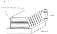
- the substrate there is used a substrate of borosilicate glass (BK7 glass substrate) and it is washed by alcohol before starting to form a film layer.
- the substrate is heated up to 300 °C in an evaporating apparatus, and on the substrate a dielectric multiple film layer is formed by laminating 9 film layers of SiO 2 and TiO 2 , as shown in Fig. 6.
- the material for the SiO 2 As the material for the SiO 2 , an SiO 2 disc of 2 inches diameter is used, and the thickness of each film of SiO 2 is about 104 nm.
- each film of TiO 2 is about 50 nm.
- the dielectric multiple film layer produced as is mentioned above has the same structure as that of the so-called “mirror of dielectric multiple film layer,” and has a peak in reflectivity at about 600 nm.
- the reflectivity is not so large with respect to light of a wavelength of 300 through 400 nm and the laser beam can sufficiently penetrate through the film layer. Therefore, a laser beam having a wavelength in this range can be used.
- the third high harmonic wavelength (355 nm) of an Nd:YAG laser is used.
- the energy of the laser beam is 350 mJ/pulse at a point just after being emitted from the laser source, the pulse width is 5 nsec, and the repetitive frequency is 5 Hz.
- the diameter of the laser beam is about 7 mm.
- This single laser beam is divided into two laser beams through a beam splitter, as shown in Fig. 1, and they are adjusted to irradiate again onto the substrate after passing through the respective different light paths.
- a beam splitter as shown in Fig. 1
- the optical distances of the two beams be substantially equal, and that the energy of the beams be about same.
- the difference in the optical distances of the two beams is less than 2 cm, and it is sufficiently small in comparison with the spatial length of the pulse of laser light, i.e., 150 cm. Therefore, it is possible to form a clear interference pattern. Further, in the present embodiment, although the energy levels in the two laser beams are different in a ration of about 1:2 due to the differences in the mirror loss at the respective light paths, the clearness of the interference pattern formed is not lost with such a difference in energy levels.
- the laser beam is focused with a lens having a focal length of 200 mm so as to obtain a beam size of about 2 mm on the substrate.
- the laser beam is irradiated under ambient atmospheric air, a discharge through the air occurs at the focus position of the lens.
- the position of the glass substrate is adjusted to be located a little bit nearer to the lens than the focus position of lens. Therefore, though the two beams in front of the lens are depicted as parallel lines in Fig. 2, they actually enter into the lens with very small incident angles respectively.
- the dielectric multiple film layer produced previously is set at the position where the interference patterns of the laser beams are formed.
- the energy of the laser beam is absorbed into the dielectric multiple film layer, and the dielectric multiple film layer, where the absorbed energy exceeds a threshold value for causing fusion, evaporation or ablation, is removed depending on the strength of the laser beam.
- a diffraction grating is formed on which a large number of dielectric convex portions are periodically aligned in one direction.
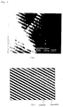
- Fig. 2(a) shows a photomicrograph of the dielectric convex portions which are formed by irradiation of the laser beam, taken by an optical microscope (X 1,000)
- Fig. 2(b) is a drawing produced on the basis of the same photo
- Fig. 7 is an enlarged perspective view of the surface of the same dielectric multiple film layer.
- the SiO 2 film layer of the plural layers comprising the dielectric multiple film layer has a low absorption coefficient with respect to the laser beam of 355 nm in the present embodiment, and that it is not easily evaporated in comparison with TiO 2 .
- the SiO 2 film layer as well as TiO 2 is evaporated, since the SiO 2 film layer which is sandwiched with TiO 2 layers at the top and bottom thereof is also heated and evaporated together with TiO 2 layers at the same time.
- the manufacturing method of the diffraction grating in accordance with the present invention can be carried out.
- the adhesion power of the film layer be strong so as to reduce damage to the film layer.
- a composition for satisfying this condition of the film layer besides SiO 2 and TiO 2 , cerium oxide, germanium oxide, magnesium fluoride, calcium fluoride, or tantalum oxide can be used.
- it is also possible to increase the strength of the adhesion by properly selecting the manufacturing method of the film, such as by selecting an ion assist electron beam evaporation method, etc.
- the interference pattern produced between the two laser beams is utilized.
- the diffraction grating produced has a periodicity along the two directions which are perpendicular to each other, as shown in Fig. 8. Namely, it is a kind of three-dimensional photonic crystal.
- a similar photonic crystal can be also realized by using the optical system as shown in Fig. 1, turning the substrate by 90 degrees, and processing it twice in the different directions.
- Fig. 4 is a schematic diagram of an apparatus for manufacturing a diffraction grating in accordance with the present invention using a phase mask
- Fig. 9(a) is a drawing for explaining the function of the phase mask
- Fig. 9(b) shows the situation where the laser beam is radiated upon the glass substrate through the same phase mask
- Fig. 9(c) shows the glass substrate which is processed by the laser beam.
- a substrate provided with the phase mask, on which the diffraction grating is formed is positioned through a spacer, and the laser beam is irradiated thereon.
- a plurality of diffraction light beams mainly included in an arc corresponding to +1 degree, 0 degree and -1 degree are emitted therefrom. Then, by the mutual interference of the diffracted light beams, a periodic optical intensity distribution is obtained in the vicinity of the emission side of the phase mask.
- phase mask having a diffraction grating frequency of 1055 nm, the depth of the diffraction grating being about 250 nm, and the size being 10 mm X 5 mm (made by QPS Technology Inc., Canada).
- the laser beam in the same manner as in Embodiment 11, there is used the third high harmonic light beam of 355 nm from an Nd:YAG laser.
- the width of the laser pulse is about 10 nsec, and the repetitive frequency thereof is 5Hz.
- the energy of the laser beam per one pulse is controlled by changing the timing of an element, the so called "Q switch", of the laser, and the laser beam which is used is set at an energy of 110 mJ/pulse, and the diameter thereof is set to about 5 mm.
- the laser beam is focused by a lens having a focal length of 250 nm, thereby obtaining a laser spot having a diameter of about 2 mm on the glass substrate.
- the distance between the phase mask and the glass substrate with the spacer is set to about 50 ⁇ m. This is for the purpose of inhibiting the adhesion of any evaporation material evaporating from the glass substrate onto the phase mask as far as possible, but the distance itself is arbitrary.
- the diffraction grating can be manufactured even if the phase mask is closely contacted with the glass substrate, and also the diffraction grating can be manufactured in a similar manner to the present embodiment even if there is inserted a quartz plate of about 150 ⁇ m thickness between the phase mask and the glass substrate, by irradiation of the laser beam thereon.
- the phase mask can be used repetitively, and therefore it is important to keep it clean from such contamination. Accordingly, it is effective to insert the spacer between them.
- the diffraction grating or the photonic crystal can be manufactured, after forming a dielectric multiple film layer on the surface of a substrate, by irradiating a laser beam having an intensity distribution onto said dielectric multiple film layer, removing a portion of the dielectric multiple film layer depending on the intensity of the laser beam, and leaving the other portions as the periodically aligned dielectric convex portions having a grating constant corresponding to the wavelength of the light.
Landscapes
- Chemical & Material Sciences (AREA)
- Engineering & Computer Science (AREA)
- General Chemical & Material Sciences (AREA)
- Geochemistry & Mineralogy (AREA)
- Life Sciences & Earth Sciences (AREA)
- Organic Chemistry (AREA)
- Optics & Photonics (AREA)
- Chemical Kinetics & Catalysis (AREA)
- Physics & Mathematics (AREA)
- Materials Engineering (AREA)
- Toxicology (AREA)
- Health & Medical Sciences (AREA)
- Plasma & Fusion (AREA)
- Mechanical Engineering (AREA)
- Diffracting Gratings Or Hologram Optical Elements (AREA)
- Laser Beam Processing (AREA)
Applications Claiming Priority (5)
| Application Number | Priority Date | Filing Date | Title |
|---|---|---|---|
| JP21339296A JP3960643B2 (ja) | 1996-08-13 | 1996-08-13 | 光学素子の製造方法 |
| JP21339296 | 1996-08-13 | ||
| JP21339196 | 1996-08-13 | ||
| JP21339196A JP3452733B2 (ja) | 1996-08-13 | 1996-08-13 | 回折型の光学素子の製造方法 |
| PCT/JP1997/002806 WO1998006676A1 (fr) | 1996-08-13 | 1997-08-11 | Procede d'usinage au laser pour substrat de verre, dispositif optique du type a diffraction fabrique par ce procede d'usinage, et procede de fabrication de ce dispositif optique |
Publications (2)
| Publication Number | Publication Date |
|---|---|
| EP0959051A1 true EP0959051A1 (fr) | 1999-11-24 |
| EP0959051A4 EP0959051A4 (en) | 1999-12-15 |
Family
ID=26519781
Family Applications (1)
| Application Number | Title | Priority Date | Filing Date |
|---|---|---|---|
| EP97934765A Withdrawn EP0959051A4 (en) | 1996-08-13 | 1997-08-11 | Laser machining method for glass substrate, diffraction type optical device fabricated by the machining method, and method of manufacturing optical device |
Country Status (3)
| Country | Link |
|---|---|
| US (3) | US6291797B1 (fr) |
| EP (1) | EP0959051A4 (fr) |
| WO (1) | WO1998006676A1 (fr) |
Cited By (10)
| Publication number | Priority date | Publication date | Assignee | Title |
|---|---|---|---|---|
| WO2001058638A1 (fr) * | 2000-02-11 | 2001-08-16 | Weston Medical Limited | Procede et appareil de fabrication d'une gelule de medicament destinee a un injecteur sans aiguille |
| DE10017614A1 (de) * | 2000-03-31 | 2001-10-25 | Laser Lab Goettingen Ev | Verfahren zur Herstellung einer dielektrischen Reflexionsmaske |
| WO2003019250A1 (fr) * | 2001-08-23 | 2003-03-06 | Cranfield University | Procede de realisation de dispositif optique a cavite |
| US6855380B2 (en) | 2001-05-18 | 2005-02-15 | Carl Zeiss Smt Ag | Method for the production of optical components with increased stability, components obtained thereby and their use |
| DE10343720A1 (de) * | 2003-09-12 | 2005-04-28 | Zeiss Carl Jena Gmbh | Polarisationsstrahlteiler auf Basis eines hochfrequenten Gitters |
| DE10355599A1 (de) * | 2003-11-28 | 2005-07-07 | Infineon Technologies Ag | Verfahren zur Herstellung eines Polarisationsgitters zur Polarisation elektromagnetischer Strahlung in einer lithographischen Belichtungseinrichtung |
| DE10132819B4 (de) * | 2001-05-18 | 2006-04-13 | Carl Zeiss Smt Ag | Verfahren zur Herstellung optischer Bauteile mit erhöhter Stabilität, damit erhaltene optische Elemente und ihre Verwendung |
| EP1724618A1 (fr) * | 2005-05-16 | 2006-11-22 | LG Electronics Inc. | Dispositif d'affichage avec feuille de polarisateur et procédé de fabrication de ladite feuille de polarisateur |
| WO2014188127A1 (fr) * | 2013-05-24 | 2014-11-27 | Saint-Gobain Glass France | Procede d'obtention d'un substrat muni d'un revetement |
| EP3031785A1 (fr) * | 2014-12-12 | 2016-06-15 | Schott AG | Procede de fabrication d'un element en vitroceramique faisant appel a un revetement structure |
Families Citing this family (68)
| Publication number | Priority date | Publication date | Assignee | Title |
|---|---|---|---|---|
| IL131037A (en) * | 1999-07-22 | 2004-06-20 | Israel Atomic Energy Comm | Method for making threedimensional photonic band-gap crystals |
| US6531679B2 (en) * | 2000-09-29 | 2003-03-11 | Siemens Aktiengesellschaft | Method for the laser machining of organic materials |
| US6830850B1 (en) * | 2001-03-16 | 2004-12-14 | Advanced Micro Devices, Inc. | Interferometric lithography using reflected light from applied layers |
| AU2003268681A1 (en) * | 2002-09-27 | 2004-05-04 | Nec Machinery Corporation | Cyclic structure formation method and surface treatment method |
| JP4156445B2 (ja) * | 2003-06-04 | 2008-09-24 | 株式会社 日立ディスプレイズ | 液晶表示装置の製造方法 |
| US7085057B2 (en) * | 2003-10-15 | 2006-08-01 | Invenios | Direct-write system and method for roll-to-roll manufacturing of reflective gratings |
| DE10350798B4 (de) * | 2003-10-29 | 2016-03-24 | Daimler Ag | Verfahren zum Betrieb einer Brennkraftmaschine |
| US6946619B2 (en) * | 2003-11-17 | 2005-09-20 | Troitski | Method and laser-computer system for producing laser-induced holograms |
| US7633033B2 (en) * | 2004-01-09 | 2009-12-15 | General Lasertronics Corporation | Color sensing for laser decoating |
| US7800014B2 (en) | 2004-01-09 | 2010-09-21 | General Lasertronics Corporation | Color sensing for laser decoating |
| JP2005279659A (ja) * | 2004-03-26 | 2005-10-13 | Toshiba Corp | レーザマーキング方法、レーザマーキング装置、マーク読取方法 |
| JP4964123B2 (ja) * | 2004-04-16 | 2012-06-27 | ディ.ケイ. アンド イー.エル. マクフェイル エンタープライジーズ プロプライエタリー リミテッド | 空洞構造を備えた、調節可能フォトニック結晶として使用される光学的活性素子の形成方法 |
| DE102004041222A1 (de) * | 2004-08-26 | 2006-03-02 | Carl Zeiss Jena Gmbh | Photonische Kristallstruktur |
| US7800823B2 (en) | 2004-12-06 | 2010-09-21 | Moxtek, Inc. | Polarization device to polarize and further control light |
| US7961393B2 (en) | 2004-12-06 | 2011-06-14 | Moxtek, Inc. | Selectively absorptive wire-grid polarizer |
| US20080055720A1 (en) * | 2006-08-31 | 2008-03-06 | Perkins Raymond T | Optical Data Storage System with an Inorganic, Dielectric Grid Polarizer |
| US20080055549A1 (en) * | 2006-08-31 | 2008-03-06 | Perkins Raymond T | Projection Display with an Inorganic, Dielectric Grid Polarizer |
| US7630133B2 (en) | 2004-12-06 | 2009-12-08 | Moxtek, Inc. | Inorganic, dielectric, grid polarizer and non-zero order diffraction grating |
| US20080055721A1 (en) * | 2006-08-31 | 2008-03-06 | Perkins Raymond T | Light Recycling System with an Inorganic, Dielectric Grid Polarizer |
| US20080055719A1 (en) * | 2006-08-31 | 2008-03-06 | Perkins Raymond T | Inorganic, Dielectric Grid Polarizer |
| US7570424B2 (en) | 2004-12-06 | 2009-08-04 | Moxtek, Inc. | Multilayer wire-grid polarizer |
| JP4791745B2 (ja) * | 2005-03-28 | 2011-10-12 | パナソニック電工株式会社 | 光学媒質の光入出射部処理方法 |
| WO2006126405A1 (fr) * | 2005-05-25 | 2006-11-30 | Sharp Kabushiki Kaisha | Substrat pour dispositif d’affichage a cristaux liquides, son procede de fabrication, dispositif d’affichage a cristaux liquides et procede de fabrication de ce dernier |
| US7486854B2 (en) | 2006-01-24 | 2009-02-03 | Uni-Pixel Displays, Inc. | Optical microstructures for light extraction and control |
| ES2325894B1 (es) | 2006-02-24 | 2010-10-28 | Universidad De Cadiz | Metodo y aparato para la fabricacion de elementos opticos difractivos. |
| ES2299335B2 (es) | 2006-03-09 | 2010-10-13 | Universidad De Cadiz | Metodo para la fabricacion de estructuras opticas con funcionalidad puramente refractivas. |
| US8755113B2 (en) | 2006-08-31 | 2014-06-17 | Moxtek, Inc. | Durable, inorganic, absorptive, ultra-violet, grid polarizer |
| JP2008070556A (ja) * | 2006-09-13 | 2008-03-27 | Nitto Denko Corp | 光学部材の製造方法および光学部材成形用型の製造方法 |
| US8536483B2 (en) * | 2007-03-22 | 2013-09-17 | General Lasertronics Corporation | Methods for stripping and modifying surfaces with laser-induced ablation |
| US20090008827A1 (en) * | 2007-07-05 | 2009-01-08 | General Lasertronics Corporation, A Corporation Of The State Of California | Aperture adapters for laser-based coating removal end-effector |
| US8003425B2 (en) * | 2008-05-14 | 2011-08-23 | International Business Machines Corporation | Methods for forming anti-reflection structures for CMOS image sensors |
| US7759755B2 (en) | 2008-05-14 | 2010-07-20 | International Business Machines Corporation | Anti-reflection structures for CMOS image sensors |
| US8248696B2 (en) | 2009-06-25 | 2012-08-21 | Moxtek, Inc. | Nano fractal diffuser |
| US20110085232A1 (en) * | 2009-10-08 | 2011-04-14 | The Penn State Research Foundation | Multi-spectral filters, mirrors and anti-reflective coatings with subwavelength periodic features for optical devices |
| TWI484224B (zh) * | 2010-03-23 | 2015-05-11 | Univ Nat Central | 液晶透鏡之製造方法、以此方法所製得之液晶透鏡、以及液晶配向基板 |
| US10112257B1 (en) | 2010-07-09 | 2018-10-30 | General Lasertronics Corporation | Coating ablating apparatus with coating removal detection |
| US8611007B2 (en) | 2010-09-21 | 2013-12-17 | Moxtek, Inc. | Fine pitch wire grid polarizer |
| US8913321B2 (en) | 2010-09-21 | 2014-12-16 | Moxtek, Inc. | Fine pitch grid polarizer |
| US9878530B2 (en) | 2010-12-30 | 2018-01-30 | 3M Innovative Properties Company | Laser cutting method and articles produced therewith |
| US8913320B2 (en) | 2011-05-17 | 2014-12-16 | Moxtek, Inc. | Wire grid polarizer with bordered sections |
| US8873144B2 (en) | 2011-05-17 | 2014-10-28 | Moxtek, Inc. | Wire grid polarizer with multiple functionality sections |
| CN102416527B (zh) * | 2011-07-29 | 2014-12-03 | 武汉理工大学 | 纳秒激光刻蚀亚波长周期性条纹的方法 |
| US9895771B2 (en) | 2012-02-28 | 2018-02-20 | General Lasertronics Corporation | Laser ablation for the environmentally beneficial removal of surface coatings |
| US8922890B2 (en) | 2012-03-21 | 2014-12-30 | Moxtek, Inc. | Polarizer edge rib modification |
| JP6007830B2 (ja) * | 2012-03-26 | 2016-10-12 | 旭硝子株式会社 | 透過型回折素子 |
| US8904822B2 (en) * | 2012-11-06 | 2014-12-09 | Corning Incorporated | Thickness control of substrates |
| US9354374B2 (en) | 2013-10-24 | 2016-05-31 | Moxtek, Inc. | Polarizer with wire pair over rib |
| US10086597B2 (en) | 2014-01-21 | 2018-10-02 | General Lasertronics Corporation | Laser film debonding method |
| EP3174662B1 (fr) | 2014-07-29 | 2021-10-20 | Gentex Corporation | Méthode d'ablation par laser à effets visuels réduits |
| US9895772B2 (en) | 2014-10-03 | 2018-02-20 | Gentex Corporation | Second surface laser ablation |
| EP3854513B1 (fr) | 2014-11-19 | 2024-01-03 | TRUMPF Laser- und Systemtechnik GmbH | Système de formation d'un faisceau optique asymétrique |
| DE102014116957A1 (de) | 2014-11-19 | 2016-05-19 | Trumpf Laser- Und Systemtechnik Gmbh | Optisches System zur Strahlformung |
| DE102014116958B9 (de) | 2014-11-19 | 2017-10-05 | Trumpf Laser- Und Systemtechnik Gmbh | Optisches System zur Strahlformung eines Laserstrahls, Laserbearbeitungsanlage, Verfahren zur Materialbearbeitung und Verwenden einer gemeinsamen langgezogenen Fokuszone zur Lasermaterialbearbeitung |
| CN108351564B (zh) * | 2015-06-19 | 2020-10-09 | 金泰克斯公司 | 第二表面激光烧蚀 |
| WO2018122208A1 (fr) * | 2016-12-30 | 2018-07-05 | Danmarks Tekniske Universitet | Modification photothermique de structures diélectriques à indice élevé |
| US11009760B2 (en) | 2017-05-05 | 2021-05-18 | Gentex Corporation | Interleaving laser ablation |
| GB2578236B (en) | 2017-05-24 | 2022-11-09 | Univ Columbia | Broadband achromatic flat optical components by dispersion-engineered dielectric metasurfaces |
| EP3636404B1 (fr) * | 2017-06-06 | 2023-11-29 | Nihon Spindle Manufacturing Co., Ltd. | Dispositif de malaxage |
| CN119781177A (zh) | 2017-08-31 | 2025-04-08 | 梅特兰兹股份有限公司 | 透射型超表面透镜集成 |
| KR102763012B1 (ko) | 2018-01-24 | 2025-02-07 | 프레지던트 앤드 펠로우즈 오브 하바드 칼리지 | 메타표면을 이용한 편광 상태 생성 |
| CN112088146A (zh) | 2018-03-06 | 2020-12-15 | 康宁公司 | 控制基板厚度的设备和方法 |
| SG11202013228XA (en) | 2018-07-02 | 2021-01-28 | Metalenz Inc | Metasurfaces for laser speckle reduction |
| KR20220035971A (ko) | 2019-07-26 | 2022-03-22 | 메탈렌츠 인코포레이티드 | 개구-메타 표면 및 하이브리드 굴절-메타 표면 이미징 시스템 |
| US11578968B1 (en) | 2019-10-31 | 2023-02-14 | President And Fellows Of Harvard College | Compact metalens depth sensors |
| EP4106618B1 (fr) * | 2020-02-19 | 2026-01-28 | Thermo Electron Scientific Instruments LLC | Masque de phase pour éclairage structuré |
| WO2022251843A1 (fr) | 2021-05-25 | 2022-12-01 | Metalenz, Inc. | Projecteur à motif de points à élément unique |
| CN120188073A (zh) | 2022-03-31 | 2025-06-20 | 梅特兰兹股份有限公司 | 偏振分选超颖表面微透镜阵列设备 |
| CN117255772A (zh) | 2022-04-19 | 2023-12-19 | 圣戈本玻璃法国公司 | 具有反射减少的表面的玻璃板及其制造方法 |
Family Cites Families (67)
| Publication number | Priority date | Publication date | Assignee | Title |
|---|---|---|---|---|
| US2751419A (en) | 1954-09-13 | 1956-06-19 | Du Pont | Process for purification of polytetramethyleneether |
| US3689933A (en) * | 1970-01-07 | 1972-09-05 | Energy Conversion Devices Inc | Apparatus employed in electrostatic printing |
| JPS5122239B2 (fr) | 1973-08-21 | 1976-07-08 | ||
| US4153786A (en) | 1977-03-30 | 1979-05-08 | E. I. Du Pont De Nemours And Company | Method for preparing ester end-capped copolyether glycols |
| US4120903A (en) | 1977-03-30 | 1978-10-17 | E. I. Du Pont De Nemours And Company | Method for preparing poly(tetramethylene ether) glycol |
| CA1216597A (fr) | 1983-05-23 | 1987-01-13 | Atsushi Aoshima | Production de polyetherglycole |
| CA1268481A (fr) | 1984-11-13 | 1990-05-01 | Atsushi Aoshima | Epuration du polyether |
| US4744615A (en) * | 1986-01-29 | 1988-05-17 | International Business Machines Corporation | Laser beam homogenizer |
| JPS6330931A (ja) | 1986-07-25 | 1988-02-09 | Nec Corp | 帳票フオ−マツト定義方式 |
| JPS6330932A (ja) | 1986-07-25 | 1988-02-09 | Ricoh Co Ltd | イメ−ジデ−タ処理装置 |
| US5007709A (en) * | 1987-12-28 | 1991-04-16 | Matsushita Electric Industrial Co., Ltd. | Diffraction grating and manufacturing method thereof |
| US5072091A (en) * | 1989-04-03 | 1991-12-10 | The Local Government Of Osaka Prefecture | Method and apparatus for metal surface process by laser beam |
| US5011565A (en) * | 1989-12-06 | 1991-04-30 | Mobil Solar Energy Corporation | Dotted contact solar cell and method of making same |
| US5537666A (en) * | 1990-09-12 | 1996-07-16 | Seiko Epson Coropration | Surface emission type semiconductor laser |
| JP2815240B2 (ja) | 1991-01-29 | 1998-10-27 | 大阪府 | 金属表面のレーザー加工方法 |
| MX9200724A (es) | 1991-02-22 | 1993-05-01 | Exxon Chemical Patents Inc | Mezcla termosellable de polietileno o plastomero de muy baja densidad con polimeros a base de polipropileno y pelicula termosellable asi como articulos hechos con aquellas. |
| JP3285214B2 (ja) * | 1991-03-22 | 2002-05-27 | 株式会社日立製作所 | レーザ加工用光学装置 |
| CA2113627A1 (fr) | 1991-07-18 | 1993-02-18 | Prasadarao Meka | Article thermoscelle |
| US5206075A (en) | 1991-12-19 | 1993-04-27 | Exxon Chemical Patents Inc. | Sealable polyolefin films containing very low density ethylene copolymers |
| US5530065A (en) | 1992-01-07 | 1996-06-25 | Exxon Chemical Patents Inc. | Heat sealable films and articles made therefrom |
| JPH05200577A (ja) * | 1992-01-22 | 1993-08-10 | Hitachi Ltd | レーザ照射装置及び照射方法 |
| JP2581373B2 (ja) * | 1992-04-27 | 1997-02-12 | 双葉電子工業株式会社 | 透明導電膜配線基板の製造方法 |
| JP3253083B2 (ja) | 1992-08-20 | 2002-02-04 | イー・アイ・デユポン・ドウ・ヌムール・アンド・カンパニー | レーザー放射線を使用して配向した重合体基質の微細構造表面を得る方法 |
| BR9307060A (pt) | 1992-09-16 | 1999-06-29 | Exxon Chemical Patents Inc | Películas macias com propriedades físicas aperfeiçoadas |
| US5482770A (en) | 1992-11-03 | 1996-01-09 | W. R. Grace & Co.-Conn. | Highly oriented multilayer film |
| ATE291059T1 (de) | 1992-11-13 | 2005-04-15 | Cryovac Inc | Wärmeschrumpfbare, durch single-site-katalyse hergestellte copolymere enthaltende folien. |
| US5604043A (en) | 1993-09-20 | 1997-02-18 | W.R. Grace & Co.-Conn. | Heat shrinkable films containing single site catalyzed copolymers having long chain branching |
| CA2085813C (fr) | 1992-12-18 | 2001-06-12 | Bankim B. Desai | Formulation pour emballage-barriere haute resistance et thermoretrecissable pour le conditionnement des viandes |
| JP2708688B2 (ja) | 1993-01-20 | 1998-02-04 | リンナイ株式会社 | ターンテーブル付天火 |
| CA2114459C (fr) * | 1993-01-29 | 1999-09-07 | Shigeaki Mizushima | Dispositif d'affichage a cristaux liquides a substrat ayant une couche d'alignement rugueux et methode de realisation |
| US5322726A (en) | 1993-03-19 | 1994-06-21 | James River Paper Company, Inc. | Coextruded film having high oxygen transmission rate |
| US5424362A (en) | 1993-04-28 | 1995-06-13 | The Dow Chemical Company | Paintable olefinic interpolymer compositions |
| US5523136A (en) | 1993-04-30 | 1996-06-04 | Cypress Packaging | Packaging film, packages and methods for using them |
| ES2235285T3 (es) | 1993-05-13 | 2005-07-01 | Exxonmobil Chemical Patents Inc. | Copolimeros de etileno con una distribucion de la composicion relativamente estrecha, su produccion y uso. |
| DE4338969C2 (de) * | 1993-06-18 | 1996-09-19 | Schott Glaswerke | Verfahren zur Herstellung anorganischer diffraktiver Elemente und Verwendung derselben |
| AU701139B2 (en) | 1993-06-24 | 1999-01-21 | Bemis Company, Inc. | Improved structures of polymers made from single site catalysts |
| US5397613A (en) | 1993-07-12 | 1995-03-14 | Viskase Corporation | Puncture resistant heat shrinkable film containing narrow molecular weight ethylene alpha olefin |
| JP3292556B2 (ja) | 1993-08-20 | 2002-06-17 | 能美防災株式会社 | スプリンクラ消火設備 |
| JPH07102470A (ja) | 1993-10-04 | 1995-04-18 | F B Tex Kk | パイル編物の製造方法 |
| US5393482A (en) * | 1993-10-20 | 1995-02-28 | United Technologies Corporation | Method for performing multiple beam laser sintering employing focussed and defocussed laser beams |
| JP3589352B2 (ja) | 1993-11-12 | 2004-11-17 | エクソンモービル・ケミカル・パテンツ・インク | ヒートシール可能なフィルム及びそれらから製造された製品 |
| ATE168631T1 (de) | 1993-12-08 | 1998-08-15 | Dow Chemical Co | Streckbarer, selbstklebender film und verfahren zur herstellung |
| GB9325468D0 (en) | 1993-12-13 | 1994-02-16 | Ici Plc | Process for purifying polyols |
| US5538790A (en) | 1993-12-17 | 1996-07-23 | Exxon Chemical Patents Inc. | Cling film |
| GB9402430D0 (en) | 1994-02-08 | 1994-03-30 | Du Pont Canada | Multilayer ethylene copolymer film |
| JPH089794A (ja) | 1994-07-01 | 1996-01-16 | Tokai Bussan Kk | 遮光用及び反射用シート |
| JP2855253B2 (ja) | 1994-07-14 | 1999-02-10 | 高島産業株式会社 | アーク溶接用ノズルクリーナー |
| JPH0857678A (ja) * | 1994-08-23 | 1996-03-05 | Seiko Epson Corp | レーザ加工装置 |
| JPH08101393A (ja) * | 1994-09-30 | 1996-04-16 | Nissan Chem Ind Ltd | 液晶配向処理方法及び液晶表示素子 |
| US5747592A (en) | 1994-12-16 | 1998-05-05 | Exxon Chemical Patents, Inc. | Thermoplastic polymer compositions and their production and use |
| DE19535503A1 (de) | 1995-09-25 | 1997-03-27 | Wolff Walsrode Ag | Siegelbare Kaschierfolie enthaltend mit Metallocen-Katalysatoren hergestellte Copolymere |
| JP3043977B2 (ja) | 1995-10-04 | 2000-05-22 | ハウス食品株式会社 | 包装袋用フィルム及びこれにより形成した包装袋 |
| JPH0999957A (ja) | 1995-10-06 | 1997-04-15 | Toppan Printing Co Ltd | 易開封性包装袋 |
| JP3167905B2 (ja) | 1995-11-20 | 2001-05-21 | 株式会社サンエー化研 | 耐熱性熱接着フィルム |
| JP3579754B2 (ja) | 1995-11-21 | 2004-10-20 | 東ソー株式会社 | 積層体及び医療用袋 |
| DE19544295A1 (de) | 1995-11-28 | 1997-06-05 | Zeiss Carl Jena Gmbh | Verfahren und Anordnung zur Erzeugung von Strukturen im Submikrometerbereich |
| JPH09150488A (ja) | 1995-11-29 | 1997-06-10 | Tokuyama Corp | 積層フィルム |
| JPH09150489A (ja) | 1995-11-30 | 1997-06-10 | Sekisui Chem Co Ltd | 多層シーラントフィルムおよびこれを用いた複合包装材料 |
| FR2744066A1 (fr) * | 1996-01-30 | 1997-08-01 | Otis Elevator Co | Procede d'impression laser |
| AU1344997A (en) | 1996-02-09 | 1997-08-28 | Tredegar Industries, Inc. | Heat sealable, peelable film and method of making same |
| EP0906181A1 (fr) | 1996-05-20 | 1999-04-07 | Union Camp Corporation | Film obtenu par coextrusion-soufflage et produits realises a l'aide de ce film |
| US5824374A (en) * | 1996-07-22 | 1998-10-20 | Optical Coating Laboratory, Inc. | In-situ laser patterning of thin film layers during sequential depositing |
| JP3270814B2 (ja) * | 1996-08-27 | 2002-04-02 | 日本板硝子株式会社 | 回折型光学素子の製造方法 |
| JPH10123357A (ja) * | 1996-10-24 | 1998-05-15 | Nippon Sheet Glass Co Ltd | 光導波路に対するレーザ加工方法 |
| JP3155717B2 (ja) * | 1996-10-24 | 2001-04-16 | 日本板硝子株式会社 | マイクロレンズに対するレーザ加工方法 |
| JP3957010B2 (ja) * | 1997-06-04 | 2007-08-08 | 日本板硝子株式会社 | 微細孔を有するガラス基材 |
| US6845114B2 (en) * | 2002-10-16 | 2005-01-18 | Eastman Kodak Company | Organic laser that is attachable to an external pump beam light source |
-
1997
- 1997-08-11 US US09/284,269 patent/US6291797B1/en not_active Expired - Fee Related
- 1997-08-11 WO PCT/JP1997/002806 patent/WO1998006676A1/fr not_active Ceased
- 1997-08-11 EP EP97934765A patent/EP0959051A4/xx not_active Withdrawn
-
2001
- 2001-07-03 US US09/898,239 patent/US6645603B2/en not_active Expired - Fee Related
-
2003
- 2003-07-18 US US10/622,517 patent/US6924457B2/en not_active Expired - Fee Related
Cited By (19)
| Publication number | Priority date | Publication date | Assignee | Title |
|---|---|---|---|---|
| WO2001058638A1 (fr) * | 2000-02-11 | 2001-08-16 | Weston Medical Limited | Procede et appareil de fabrication d'une gelule de medicament destinee a un injecteur sans aiguille |
| DE10017614A1 (de) * | 2000-03-31 | 2001-10-25 | Laser Lab Goettingen Ev | Verfahren zur Herstellung einer dielektrischen Reflexionsmaske |
| DE10017614B4 (de) * | 2000-03-31 | 2005-02-24 | Laser-Laboratorium Göttingen eV | Verfahren zur Herstellung einer dielektrischen Reflexionsmaske |
| US6855380B2 (en) | 2001-05-18 | 2005-02-15 | Carl Zeiss Smt Ag | Method for the production of optical components with increased stability, components obtained thereby and their use |
| DE10132819B4 (de) * | 2001-05-18 | 2006-04-13 | Carl Zeiss Smt Ag | Verfahren zur Herstellung optischer Bauteile mit erhöhter Stabilität, damit erhaltene optische Elemente und ihre Verwendung |
| WO2003019250A1 (fr) * | 2001-08-23 | 2003-03-06 | Cranfield University | Procede de realisation de dispositif optique a cavite |
| DE10343720A1 (de) * | 2003-09-12 | 2005-04-28 | Zeiss Carl Jena Gmbh | Polarisationsstrahlteiler auf Basis eines hochfrequenten Gitters |
| DE10355599B4 (de) * | 2003-11-28 | 2009-05-14 | Qimonda Ag | Verfahren zur Durchführung einer lithographischen Belichtung mithilfe polarisierter elektromagnetischer Strahlung in einer lithographischen Belichtungseinrichtung |
| DE10355599A1 (de) * | 2003-11-28 | 2005-07-07 | Infineon Technologies Ag | Verfahren zur Herstellung eines Polarisationsgitters zur Polarisation elektromagnetischer Strahlung in einer lithographischen Belichtungseinrichtung |
| EP1724618A1 (fr) * | 2005-05-16 | 2006-11-22 | LG Electronics Inc. | Dispositif d'affichage avec feuille de polarisateur et procédé de fabrication de ladite feuille de polarisateur |
| CN100464201C (zh) * | 2005-05-16 | 2009-02-25 | Lg电子株式会社 | 带有偏振器片的显示设备和制造偏振器片的方法 |
| WO2014188127A1 (fr) * | 2013-05-24 | 2014-11-27 | Saint-Gobain Glass France | Procede d'obtention d'un substrat muni d'un revetement |
| FR3005878A1 (fr) * | 2013-05-24 | 2014-11-28 | Saint Gobain | Procede d'obtention d'un substrat muni d'un revetement |
| CN105392591A (zh) * | 2013-05-24 | 2016-03-09 | 法国圣戈班玻璃厂 | 用于获得提供有涂层的基材的方法 |
| CN105392591B (zh) * | 2013-05-24 | 2018-01-26 | 法国圣戈班玻璃厂 | 用于获得提供有涂层的基材的方法 |
| TWI632973B (zh) * | 2013-05-24 | 2018-08-21 | 法國聖戈本玻璃公司 | 配置有塗層之基板、其用途及製得彼的設備及方法 |
| US10301712B2 (en) | 2013-05-24 | 2019-05-28 | Saint-Gobain Glass France | Process for obtaining a substrate provided with a coating |
| EP3031785A1 (fr) * | 2014-12-12 | 2016-06-15 | Schott AG | Procede de fabrication d'un element en vitroceramique faisant appel a un revetement structure |
| US10315276B2 (en) | 2014-12-12 | 2019-06-11 | Schott Ag | Method for producing a glass ceramic element with patterned coating |
Also Published As
| Publication number | Publication date |
|---|---|
| US6924457B2 (en) | 2005-08-02 |
| US20020040892A1 (en) | 2002-04-11 |
| WO1998006676A1 (fr) | 1998-02-19 |
| US6645603B2 (en) | 2003-11-11 |
| US6291797B1 (en) | 2001-09-18 |
| EP0959051A4 (en) | 1999-12-15 |
| US20040031778A1 (en) | 2004-02-19 |
Similar Documents
| Publication | Publication Date | Title |
|---|---|---|
| US6645603B2 (en) | Laser processing method to a glass substrate and an optical diffraction element obtained thereby, and a method for manufacturing optical elements | |
| US5910256A (en) | Method for manufacturing a diffraction type optical element | |
| US5018164A (en) | Excimer laser ablation method and apparatus for microcircuit fabrication | |
| JP4124396B2 (ja) | ホログラムの製造方法および装置 | |
| US5241417A (en) | Multi-layered optical filter film and production method thereof | |
| JP3907709B2 (ja) | 無機回折素子の製造方法 | |
| JP4269295B2 (ja) | 微細構造体の製造方法 | |
| JP2003057422A (ja) | フェムト秒レーザー照射による周期微細構造の作成方法 | |
| JP3960643B2 (ja) | 光学素子の製造方法 | |
| JP3452733B2 (ja) | 回折型の光学素子の製造方法 | |
| JP3426154B2 (ja) | グレーティング付き光導波路の製造方法 | |
| CN117381146B (zh) | 一种基于硫系材料的激光加工方法及集成光子器件 | |
| US6368775B1 (en) | 3-D photo-patterning of refractive index structures in photosensitive thin film materials | |
| US6645893B2 (en) | Glass suitable for optical functional elements and process for producing same | |
| Takao et al. | Microlenses fabricated on silicone rubber using F2 Laser | |
| EP2000558B1 (fr) | Procédé et appareil de fabrication de structures optiques de réfraction pure | |
| Mizeikis et al. | Silicon surface processing techniques for micro-systems fabrication | |
| US4612234A (en) | Anti-reflection coating film suitable for application on optics made of mixed crystals of thallium iodide and thallium bromide | |
| US6744560B2 (en) | Non-linear optical material | |
| Thönissen et al. | Improved interference filter structures made of porous silicon | |
| Klein-Wiele et al. | Fabrication of SiO2 phase gratings by UV laser patterning of silicon suboxide layers and subsequent oxidation | |
| CN117248269A (zh) | 一种分子束外延设备上保护衬底的透过式主挡板 | |
| CN119179135A (zh) | 一种片上硫系倒脊型光波导及其Bragg光栅制备方法 | |
| Nishii et al. | Enormous photon-induced volume expansion of Ge-doped silica thin films | |
| Baldacchini et al. | Green-red light generation and propagation in LiF films |
Legal Events
| Date | Code | Title | Description |
|---|---|---|---|
| PUAI | Public reference made under article 153(3) epc to a published international application that has entered the european phase |
Free format text: ORIGINAL CODE: 0009012 |
|
| 17P | Request for examination filed |
Effective date: 19990315 |
|
| AK | Designated contracting states |
Kind code of ref document: A1 Designated state(s): DE FR GB IT |
|
| A4 | Supplementary search report drawn up and despatched |
Effective date: 19991102 |
|
| AK | Designated contracting states |
Kind code of ref document: A4 Designated state(s): DE FR GB IT |
|
| RIC1 | Information provided on ipc code assigned before grant |
Free format text: 6C 03C 17/22 A, 6C 03C 17/34 B, 6B 23K 26/06 B, 6G 02B 5/18 B, 6C 03C 23/00 B, 6C 03C 17/00 B |
|
| 17Q | First examination report despatched |
Effective date: 20010405 |
|
| RTI1 | Title (correction) |
Free format text: LASER MACHINING METHOD FOR MANUFACTURING AN OPTICAL ELEMENT |
|
| GRAP | Despatch of communication of intention to grant a patent |
Free format text: ORIGINAL CODE: EPIDOSNIGR1 |
|
| STAA | Information on the status of an ep patent application or granted ep patent |
Free format text: STATUS: THE APPLICATION IS DEEMED TO BE WITHDRAWN |
|
| 18D | Application deemed to be withdrawn |
Effective date: 20040831 |