EP0959648B1 - Carte imprimee et son procede de production - Google Patents
Carte imprimee et son procede de production Download PDFInfo
- Publication number
- EP0959648B1 EP0959648B1 EP98900160A EP98900160A EP0959648B1 EP 0959648 B1 EP0959648 B1 EP 0959648B1 EP 98900160 A EP98900160 A EP 98900160A EP 98900160 A EP98900160 A EP 98900160A EP 0959648 B1 EP0959648 B1 EP 0959648B1
- Authority
- EP
- European Patent Office
- Prior art keywords
- joining
- hole
- printed wiring
- wiring board
- ball
- Prior art date
- Legal status (The legal status is an assumption and is not a legal conclusion. Google has not performed a legal analysis and makes no representation as to the accuracy of the status listed.)
- Expired - Lifetime
Links
Images







Classifications
-
- H—ELECTRICITY
- H10—SEMICONDUCTOR DEVICES; ELECTRIC SOLID-STATE DEVICES NOT OTHERWISE PROVIDED FOR
- H10W—GENERIC PACKAGES, INTERCONNECTIONS, CONNECTORS OR OTHER CONSTRUCTIONAL DETAILS OF DEVICES COVERED BY CLASS H10
- H10W70/00—Package substrates; Interposers; Redistribution layers [RDL]
- H10W70/60—Insulating or insulated package substrates; Interposers; Redistribution layers
- H10W70/62—Insulating or insulated package substrates; Interposers; Redistribution layers characterised by their interconnections
- H10W70/63—Vias, e.g. via plugs
- H10W70/635—Through-vias
-
- H—ELECTRICITY
- H05—ELECTRIC TECHNIQUES NOT OTHERWISE PROVIDED FOR
- H05K—PRINTED CIRCUITS; CASINGS OR CONSTRUCTIONAL DETAILS OF ELECTRIC APPARATUS; MANUFACTURE OF ASSEMBLAGES OF ELECTRICAL COMPONENTS
- H05K3/00—Apparatus or processes for manufacturing printed circuits
- H05K3/30—Assembling printed circuits with electric components, e.g. with resistors
- H05K3/32—Assembling printed circuits with electric components, e.g. with resistors electrically connecting electric components or wires to printed circuits
- H05K3/34—Assembling printed circuits with electric components, e.g. with resistors electrically connecting electric components or wires to printed circuits by soldering
- H05K3/341—Surface mounted components
- H05K3/3421—Leaded components
- H05K3/3426—Leaded components characterised by the leads
-
- H—ELECTRICITY
- H05—ELECTRIC TECHNIQUES NOT OTHERWISE PROVIDED FOR
- H05K—PRINTED CIRCUITS; CASINGS OR CONSTRUCTIONAL DETAILS OF ELECTRIC APPARATUS; MANUFACTURE OF ASSEMBLAGES OF ELECTRICAL COMPONENTS
- H05K3/00—Apparatus or processes for manufacturing printed circuits
- H05K3/30—Assembling printed circuits with electric components, e.g. with resistors
- H05K3/32—Assembling printed circuits with electric components, e.g. with resistors electrically connecting electric components or wires to printed circuits
- H05K3/34—Assembling printed circuits with electric components, e.g. with resistors electrically connecting electric components or wires to printed circuits by soldering
- H05K3/341—Surface mounted components
- H05K3/3431—Leadless components
- H05K3/3436—Leadless components having an array of bottom contacts, e.g. pad grid array or ball grid array components
-
- H—ELECTRICITY
- H05—ELECTRIC TECHNIQUES NOT OTHERWISE PROVIDED FOR
- H05K—PRINTED CIRCUITS; CASINGS OR CONSTRUCTIONAL DETAILS OF ELECTRIC APPARATUS; MANUFACTURE OF ASSEMBLAGES OF ELECTRICAL COMPONENTS
- H05K3/00—Apparatus or processes for manufacturing printed circuits
- H05K3/36—Assembling printed circuits with other printed circuits
- H05K3/368—Assembling printed circuits with other printed circuits parallel to each other
-
- H—ELECTRICITY
- H10—SEMICONDUCTOR DEVICES; ELECTRIC SOLID-STATE DEVICES NOT OTHERWISE PROVIDED FOR
- H10W—GENERIC PACKAGES, INTERCONNECTIONS, CONNECTORS OR OTHER CONSTRUCTIONAL DETAILS OF DEVICES COVERED BY CLASS H10
- H10W90/00—Package configurations
- H10W90/401—Package configurations characterised by multiple insulating or insulated package substrates, interposers or RDLs
-
- H—ELECTRICITY
- H10—SEMICONDUCTOR DEVICES; ELECTRIC SOLID-STATE DEVICES NOT OTHERWISE PROVIDED FOR
- H10W—GENERIC PACKAGES, INTERCONNECTIONS, CONNECTORS OR OTHER CONSTRUCTIONAL DETAILS OF DEVICES COVERED BY CLASS H10
- H10W90/00—Package configurations
- H10W90/701—Package configurations characterised by the relative positions of pads or connectors relative to package parts
-
- H—ELECTRICITY
- H05—ELECTRIC TECHNIQUES NOT OTHERWISE PROVIDED FOR
- H05K—PRINTED CIRCUITS; CASINGS OR CONSTRUCTIONAL DETAILS OF ELECTRIC APPARATUS; MANUFACTURE OF ASSEMBLAGES OF ELECTRICAL COMPONENTS
- H05K2201/00—Indexing scheme relating to printed circuits covered by H05K1/00
- H05K2201/09—Shape and layout
- H05K2201/09209—Shape and layout details of conductors
- H05K2201/09372—Pads and lands
- H05K2201/09481—Via in pad; Pad over filled via
-
- H—ELECTRICITY
- H05—ELECTRIC TECHNIQUES NOT OTHERWISE PROVIDED FOR
- H05K—PRINTED CIRCUITS; CASINGS OR CONSTRUCTIONAL DETAILS OF ELECTRIC APPARATUS; MANUFACTURE OF ASSEMBLAGES OF ELECTRICAL COMPONENTS
- H05K2201/00—Indexing scheme relating to printed circuits covered by H05K1/00
- H05K2201/10—Details of components or other objects attached to or integrated in a printed circuit board
- H05K2201/10227—Other objects, e.g. metallic pieces
- H05K2201/10234—Metallic balls
-
- H—ELECTRICITY
- H05—ELECTRIC TECHNIQUES NOT OTHERWISE PROVIDED FOR
- H05K—PRINTED CIRCUITS; CASINGS OR CONSTRUCTIONAL DETAILS OF ELECTRIC APPARATUS; MANUFACTURE OF ASSEMBLAGES OF ELECTRICAL COMPONENTS
- H05K2201/00—Indexing scheme relating to printed circuits covered by H05K1/00
- H05K2201/10—Details of components or other objects attached to or integrated in a printed circuit board
- H05K2201/10227—Other objects, e.g. metallic pieces
- H05K2201/1031—Surface mounted metallic connector elements
- H05K2201/10318—Surface mounted metallic pins
-
- H—ELECTRICITY
- H05—ELECTRIC TECHNIQUES NOT OTHERWISE PROVIDED FOR
- H05K—PRINTED CIRCUITS; CASINGS OR CONSTRUCTIONAL DETAILS OF ELECTRIC APPARATUS; MANUFACTURE OF ASSEMBLAGES OF ELECTRICAL COMPONENTS
- H05K2201/00—Indexing scheme relating to printed circuits covered by H05K1/00
- H05K2201/10—Details of components or other objects attached to or integrated in a printed circuit board
- H05K2201/10431—Details of mounted components
- H05K2201/10439—Position of a single component
- H05K2201/10477—Inverted
-
- H—ELECTRICITY
- H05—ELECTRIC TECHNIQUES NOT OTHERWISE PROVIDED FOR
- H05K—PRINTED CIRCUITS; CASINGS OR CONSTRUCTIONAL DETAILS OF ELECTRIC APPARATUS; MANUFACTURE OF ASSEMBLAGES OF ELECTRICAL COMPONENTS
- H05K2201/00—Indexing scheme relating to printed circuits covered by H05K1/00
- H05K2201/10—Details of components or other objects attached to or integrated in a printed circuit board
- H05K2201/10613—Details of electrical connections of non-printed components, e.g. special leads
- H05K2201/10621—Components characterised by their electrical contacts
- H05K2201/10666—Plated through-hole for surface mounting on PCB
-
- H—ELECTRICITY
- H05—ELECTRIC TECHNIQUES NOT OTHERWISE PROVIDED FOR
- H05K—PRINTED CIRCUITS; CASINGS OR CONSTRUCTIONAL DETAILS OF ELECTRIC APPARATUS; MANUFACTURE OF ASSEMBLAGES OF ELECTRICAL COMPONENTS
- H05K2201/00—Indexing scheme relating to printed circuits covered by H05K1/00
- H05K2201/10—Details of components or other objects attached to or integrated in a printed circuit board
- H05K2201/10613—Details of electrical connections of non-printed components, e.g. special leads
- H05K2201/10742—Details of leads
- H05K2201/1075—Shape details
- H05K2201/10871—Leads having an integral insert stop
-
- H—ELECTRICITY
- H05—ELECTRIC TECHNIQUES NOT OTHERWISE PROVIDED FOR
- H05K—PRINTED CIRCUITS; CASINGS OR CONSTRUCTIONAL DETAILS OF ELECTRIC APPARATUS; MANUFACTURE OF ASSEMBLAGES OF ELECTRICAL COMPONENTS
- H05K3/00—Apparatus or processes for manufacturing printed circuits
- H05K3/30—Assembling printed circuits with electric components, e.g. with resistors
- H05K3/306—Assembling printed circuits with electric components, e.g. with resistors with lead-in-hole components
- H05K3/308—Adaptations of leads
-
- H—ELECTRICITY
- H10—SEMICONDUCTOR DEVICES; ELECTRIC SOLID-STATE DEVICES NOT OTHERWISE PROVIDED FOR
- H10W—GENERIC PACKAGES, INTERCONNECTIONS, CONNECTORS OR OTHER CONSTRUCTIONAL DETAILS OF DEVICES COVERED BY CLASS H10
- H10W70/00—Package substrates; Interposers; Redistribution layers [RDL]
- H10W70/60—Insulating or insulated package substrates; Interposers; Redistribution layers
- H10W70/62—Insulating or insulated package substrates; Interposers; Redistribution layers characterised by their interconnections
- H10W70/65—Shapes or dispositions of interconnections
- H10W70/654—Top-view layouts
- H10W70/655—Fan-out layouts
-
- H—ELECTRICITY
- H10—SEMICONDUCTOR DEVICES; ELECTRIC SOLID-STATE DEVICES NOT OTHERWISE PROVIDED FOR
- H10W—GENERIC PACKAGES, INTERCONNECTIONS, CONNECTORS OR OTHER CONSTRUCTIONAL DETAILS OF DEVICES COVERED BY CLASS H10
- H10W70/00—Package substrates; Interposers; Redistribution layers [RDL]
- H10W70/60—Insulating or insulated package substrates; Interposers; Redistribution layers
- H10W70/67—Insulating or insulated package substrates; Interposers; Redistribution layers characterised by their insulating layers or insulating parts
- H10W70/68—Shapes or dispositions thereof
- H10W70/682—Shapes or dispositions thereof comprising holes having chips therein
-
- H—ELECTRICITY
- H10—SEMICONDUCTOR DEVICES; ELECTRIC SOLID-STATE DEVICES NOT OTHERWISE PROVIDED FOR
- H10W—GENERIC PACKAGES, INTERCONNECTIONS, CONNECTORS OR OTHER CONSTRUCTIONAL DETAILS OF DEVICES COVERED BY CLASS H10
- H10W70/00—Package substrates; Interposers; Redistribution layers [RDL]
- H10W70/60—Insulating or insulated package substrates; Interposers; Redistribution layers
- H10W70/67—Insulating or insulated package substrates; Interposers; Redistribution layers characterised by their insulating layers or insulating parts
- H10W70/68—Shapes or dispositions thereof
- H10W70/685—Shapes or dispositions thereof comprising multiple insulating layers
-
- H—ELECTRICITY
- H10—SEMICONDUCTOR DEVICES; ELECTRIC SOLID-STATE DEVICES NOT OTHERWISE PROVIDED FOR
- H10W—GENERIC PACKAGES, INTERCONNECTIONS, CONNECTORS OR OTHER CONSTRUCTIONAL DETAILS OF DEVICES COVERED BY CLASS H10
- H10W72/00—Interconnections or connectors in packages
- H10W72/071—Connecting or disconnecting
- H10W72/075—Connecting or disconnecting of bond wires
- H10W72/07551—Connecting or disconnecting of bond wires characterised by changes in properties of the bond wires during the connecting
- H10W72/07554—Connecting or disconnecting of bond wires characterised by changes in properties of the bond wires during the connecting changes in dispositions
-
- H—ELECTRICITY
- H10—SEMICONDUCTOR DEVICES; ELECTRIC SOLID-STATE DEVICES NOT OTHERWISE PROVIDED FOR
- H10W—GENERIC PACKAGES, INTERCONNECTIONS, CONNECTORS OR OTHER CONSTRUCTIONAL DETAILS OF DEVICES COVERED BY CLASS H10
- H10W72/00—Interconnections or connectors in packages
- H10W72/50—Bond wires
- H10W72/541—Dispositions of bond wires
- H10W72/547—Dispositions of multiple bond wires
-
- H—ELECTRICITY
- H10—SEMICONDUCTOR DEVICES; ELECTRIC SOLID-STATE DEVICES NOT OTHERWISE PROVIDED FOR
- H10W—GENERIC PACKAGES, INTERCONNECTIONS, CONNECTORS OR OTHER CONSTRUCTIONAL DETAILS OF DEVICES COVERED BY CLASS H10
- H10W72/00—Interconnections or connectors in packages
- H10W72/851—Dispositions of multiple connectors or interconnections
- H10W72/874—On different surfaces
- H10W72/884—Die-attach connectors and bond wires
-
- H—ELECTRICITY
- H10—SEMICONDUCTOR DEVICES; ELECTRIC SOLID-STATE DEVICES NOT OTHERWISE PROVIDED FOR
- H10W—GENERIC PACKAGES, INTERCONNECTIONS, CONNECTORS OR OTHER CONSTRUCTIONAL DETAILS OF DEVICES COVERED BY CLASS H10
- H10W90/00—Package configurations
- H10W90/701—Package configurations characterised by the relative positions of pads or connectors relative to package parts
- H10W90/731—Package configurations characterised by the relative positions of pads or connectors relative to package parts of die-attach connectors
- H10W90/734—Package configurations characterised by the relative positions of pads or connectors relative to package parts of die-attach connectors between a chip and a stacked insulating package substrate, interposer or RDL
-
- H—ELECTRICITY
- H10—SEMICONDUCTOR DEVICES; ELECTRIC SOLID-STATE DEVICES NOT OTHERWISE PROVIDED FOR
- H10W—GENERIC PACKAGES, INTERCONNECTIONS, CONNECTORS OR OTHER CONSTRUCTIONAL DETAILS OF DEVICES COVERED BY CLASS H10
- H10W90/00—Package configurations
- H10W90/701—Package configurations characterised by the relative positions of pads or connectors relative to package parts
- H10W90/731—Package configurations characterised by the relative positions of pads or connectors relative to package parts of die-attach connectors
- H10W90/736—Package configurations characterised by the relative positions of pads or connectors relative to package parts of die-attach connectors between a chip and a stacked lead frame, conducting package substrate or heat sink
-
- Y—GENERAL TAGGING OF NEW TECHNOLOGICAL DEVELOPMENTS; GENERAL TAGGING OF CROSS-SECTIONAL TECHNOLOGIES SPANNING OVER SEVERAL SECTIONS OF THE IPC; TECHNICAL SUBJECTS COVERED BY FORMER USPC CROSS-REFERENCE ART COLLECTIONS [XRACs] AND DIGESTS
- Y02—TECHNOLOGIES OR APPLICATIONS FOR MITIGATION OR ADAPTATION AGAINST CLIMATE CHANGE
- Y02P—CLIMATE CHANGE MITIGATION TECHNOLOGIES IN THE PRODUCTION OR PROCESSING OF GOODS
- Y02P70/00—Climate change mitigation technologies in the production process for final industrial or consumer products
- Y02P70/50—Manufacturing or production processes characterised by the final manufactured product
Definitions
- the present invention relates to a printed wiring board and its manufacturing method, and particularly relates to joining of the printed wiring board and a mother board.
- FIG. 27 there is conventionally a printed wiring board having a circuit substrate 96 having a mounting portion 97 for mounting an electronic part 970 thereto, a conductor circuit 95 arranged on a surface of the circuit substrate 96 and also arranged within this circuit substrate 96, and a through hole 93 extending through the circuit substrate 96.
- the electronic part 970 is electrically connected to the conductor circuit 95 by a bonding wire 971.
- a pad 92 for mounting a ball thereto is arranged at an end tip of the conductor circuit 95 on a rear face side of the circuit substrate 96.
- a soldering ball 91 is joined to a surface of this pad 92.
- the above conventional printed wiring board 9 is joined to an opposite party pad 981 arranged on the surface of a mother board 98 by heating and melting the above soldering ball 91.
- the printed wiring board fulfills a function from the above structure for transmitting electric information of the electric part to a partner member such as the mother board, etc.
- the above conventional printed wiring board has the following problems.
- the printed wiring board 9 is fixedly joined onto the mother board 98 by the soldering ball 91. Therefore, the pad 92 for mounting the soldering ball must be arranged in the printed wiring board 9.
- soldering ball 91 When the soldering ball 91 is joined to the opposite party pad 981, it is difficult to control a melting state of the soldering ball 91. In particular, the soldering ball 91 is melted and joined by heating this soldering ball 91 to the opposite party pad 981 on the mother board 98. At this time, the melting state of the soldering ball 91 is different according to the elements such as heating temperature, applied pressure, soldering composition, etc. Therefore, as shown in FIG. 27, there is a case in which a melting degree of the soldering ball 91 on one side (e.g., a right-hand side of FIG.
- the melting degree of the soldering ball 91 on the other side e.g., a left-hand side of FIG. 27
- the printed wiring board 9 is joined slantingly to the mother board 98. Accordingly, it is difficult to join the conventional printed wiring board 9 to the mother board 98 in parallel with this mother board 98.
- the pad 92 for mounting the ball and joining the soldering ball 91 is generally covered with a gold plating film 921.
- a gold component of the gold plating film 921 permeates the interior of the soldering ball 91 in heating and melting the soldering ball 91, and forms an intermediate layer 90 between the metallic plating film 921 and the soldering ball 91.
- This intermediate layer 90 has a property which deteriorates by heat. Therefore, when the intermediate layer 90 is formed, joining strength of the pad 92 for mounting the ball and the soldering ball 91 is reduced from 1.0 to 1.4 kg/cm 2 .
- the intermediate layer 90 increases in thickness as the gold plating film 921 covering the pad 92 for mounting ball increases in thickness. Therefore, When the thickness of the gold plating film 921 is increased, the joining strength of the pad 92 for mounting the ball and the soldering ball 91 is further reduced. Accordingly, there is a case in which the joining strength is reduced to a joining strength equal to or smaller than 1.0 kg/cm 2 .
- the present invention provides a printed wiring board able to perform high density wiring on a substrate surface and be joined to a partner member in parallel with this partner member which has an excellent joining strength, and also provides a manufacturing method for the printed wiring board.
- AT 401 704 B discloses a carrier plate for an integrated circuit.
- JP 2 239 577 discloses a hybrid integrated circuit for surface mounting.
- JP 2 144 945 discloses a board for semiconductor mounting and its manufacture.
- FR 257 1547 discloses a hybrid circuit which can be transferred to a support containing a high-density interconnection network.
- JP 6 045 722 discloses a pin-erected type printed circuit substrate.
- the present invention comprises a printed wiring board having a circuit substrate having a conductor circuit and a through hole, and a joining pin inserted into said through hole; the printed wiring board being characterized in that said joining pin is manufactured by using a material unmelted at a heating temperature in joining the joining pin to an opposite party pad, and is constructed by a joining head portion greater than an opening diameter of said through hole and forming a joining portion to said opposite party pad, and a leg portion having a size capable of inserting this leg portion into said through hole, and the leg portion is inserted into said through hole and is joined to the through hole by a conductive material.
- the joining pin is inserted into the through hole.
- the joining pin has the joining head portion for joining the joining pin to the opposite party pad. Therefore, the through hole and the opposite party pad can be electrically connected to each other from the joining pin by joining the joining head portion to the opposite party pad.
- the through hole and the opposite party pad can be connected to each other from the joining pin in a facing state, it is unnecessary to arrange as in the conventional case a pad for mounting a soldering ball in addition to the through hole. It is also unnecessary to form a conductor circuit for connecting the through hole and the pad for mounting the ball as in the conventional case. Therefore, a surplus space is formed on a surface of the circuit substrate in a portion except for an opening portion of the through hole. Accordingly, a high density wiring structure can be realized on the substrate surface by forming many other conductor circuits in this space.
- the joining pin is manufactured by using an unmelted material at the heating temperature in joining the joining pin to the opposite party pad. Therefore, a constant height of the joining head portion is maintained without melting deformation in the above joining. Accordingly, the joining head portion functions as a strut of the printed wiring board at the joining time.
- Such a joining head portion functioning as a strut is greater than the opening diameter of the through hole Therefore, when the leg portion of the joining pin is inserted into the through hole, the joining head portion is engaged wi th the opening portion of the through hole and does not enter the interior of the through hole. Accordingly, the joining head portion can project by the same height from a surface of the circuit substrate.
- the distance between the printed wiring board and a partner member such as a mother board having the above opposite party pad, etc. is constantly secured by the above joining head portion. Accordingly, the printed wiring board can be joined to the partner member in a parallel arranged state.
- the leg portion of the joining pin is inserted into the through hole, and the leg portion and the through hole are joined to each other by the conductive material. Further, since the printed wiring board of the present invention has no structure for joining a soldering ball to the pad for mounting the ball as in the conventional example, there is no fear that an intermediate layer causing a reduction in joining strength is formed between the soldering ball and the pad for mounting the ball. Accordingly, the joining pin can be strongly fixed to the through hole.
- the joining head portion of the above joining pin It is preferable to cover the joining head portion of the above joining pin with the conductive material as described in claim 2.
- this joining head portion is arranged on the opposite party pad on the partner member and is heated, the conductive material covering a surface of the joining head portion is melted so that the joining head portion and the opposite party pad are joined to each other. Accordingly, the joining head portion and the opposite party pad can reliably be joined to each other so that the printed wiring board can be easily mounted to the partner member.
- the above leg portion has projecting portions projected in plural directions.
- a clearance having a wavy shape in cross section is formed within the through hole between the plural projecting portions in the leg portion.
- the leg portion is reliably joined to an inner wall of the through hole by the conductive material in this wavy clearance. Accordingly, the joining pin can be strongly fixed to the through hole.
- the above joining head portion is preferably constructed by a spherical body as described in claim 3.
- the joining head portion of the joining pin can be stably joined to the opposite party pad.
- the manufacturing method comprises:
- the leg portion of the joining pin is inserted into the through hole.
- the joining pin has the joining head portion for joining the joining pin to the opposite party pad. Therefore, in accordance with the manufacturing method of the present invention, it is possible to obtain a printed wiring board for electrically connecting the through hole and the opposite party pad to each other by the joining pin. Therefore, it is not necessary to arrange the pad for mounting a ball, etc. as in the conventional case. Accordingly, another conductor circuit can be further formed in a surplus space formed on a surface of the circuit substrate so that high density wiring can be performed
- the joining pin is manufactured by using a material unmelted in joining the joining pin to the opposite party pad. Therefore, it is possible to obtain a printed wiring board able to be joined to a partner member, etc. in parallel with this partner member. Further, since the joining pin is joined to the through hole by the conductive material by inserting the joining head portion of the joining pin into the through hole, joining strength to the opposite party pad is high.
- the joining head portion of the above joining pin it is preferable to cover the joining head portion of the above joining pin with the conductive material in advance before the joining head portion is inserted into the through hole.
- the printed wiring board can be reliably and easily mounted to the partner member.
- the above conductive member is preferably a soldering member.
- the leg portion of the joining pin can be reliably joined to the through hole and electric conductivity between the leg port ion and the through hole is improved.
- the above conductive material may be constructed by epoxy resin impregnated with a silver filler as in the invention of claims 7 and 9.
- the leg portion of the joining pin can be joined reliably to the through hole and the electric conductivity between the leg portion and the through hole is improved.
- Such an example is a printed wiring board having a circuit substrate having a conductor circuit and a through hole, and a joining ball joined to said through hole; the printed wiring board being characterized in that said joining ball is manufactured by using a material unmelted at a heating temperature in joining the joining ball to an opposite party pad, and is constructed by a joining head portion greater than an opening portion of said through hole and forming a joining portion to said opposite party pad, and a bottomportion facing the opening portion of said through hole, and the bottom portion is arranged in the opening portion of said through hole and is joined to the through hole by a conductive material filling the interior of the through hole.
- the joining ball having the joining head portion is joined to the through hole and the bottom portion of the joining ball is joined to the through hole by the conductive material filling the interior of the through hole.
- the above joining ball has the joining head portion for joining the joining ball to the opposite party pad and also has the bottom portion facing the opening portion of the through hole.
- the joining head portion is a portion greater than a diameter of the opening portion of the through hole and projecting from the through hole.
- the bottom portion is a portion facing the opening portion and joined to the through hole by the conductive material.
- the joining ball is joined to the through hole.
- the joining ball has the joining head portion for joining the joining ball to the opposite party pad. Therefore, the through hole and the opposite party pad can be electrically connected to each other by the joining ball by joining the joining head portion to the opposite party pad.
- the joining ball is joined to the opening portion of the through hole. Therefore, the through hole and the opposite party pad can be electrically connected to each other in a facing state. Accordingly, it is unnecessary to arrange a pad for mounting a soldering ball in addition to the through hole as in the conventional case.
- a surplus space is formed on a surface of the circuit substrate in a portion except for the opening portion of the through hole. Accordingly, many other conductor circuits can be formed in this space so that a high density wiring structure can be realized on the substrate surface.
- the joining ball is manufactured by using a material unmelted at the heating temperature in joining the joining ball to the opposite party pad. Therefore, a constant height of the joining ball is maintained without melting deformation in the above joining. Accordingly, the joining ball functions as a strut of the printed wiring board at the joining time.
- the joining head portion of such a joining ball functioning as a strut is greater than the opening portion of the through hole. Therefore, when the joining ball is joined to the through hole as in the conventional example, the joining head portion is engaged with the opening portion of the through hole and does not enter the interior of the through hole. Accordingly, the joining head portion can project by the same height from a surface of the circuit substrate.
- the distance between the printed wiring board and a partner member such as a mother board having the above opposite party pad, etc. is constantly secured by the above joining head portion. Accordingly, the printed wiring board can be joined to the partner member in a parallel arranging state.
- the joining ball is arranged in the opening portion of the through hole, and the joining ball and the through hole are joined to each other by the conductive material. Further, since the printed wiring board of the present invention has no structure for joining a soldering ball to the pad for mounting the ball as in the conventional example, there is no fear that an intermediate layer causing a reduction in joining strength is formed between the soldering ball and the pad for mounting the ball. Accordingly, the joining ball can be strongly fixed to the through hole.
- the joining head portion when the joining head portion is arranged on the opposite party pad on the mother board and is heated, the conductive material covering a surface of the joining head portion is melted so that the joining head portion and the opposite party pad are easily joined to each other. Accordingly, the joining head portion and the opposite party pad can be reliably joined to each other so that the printed wiring board can be easily mounted to the partner member, etc.
- the above joining head portion is preferably set to a spherical body.
- the joining head portion of the joining ball can be stably joined to the opposite party pad on the mother board.
- the bottom portion of the joining ball may also be constructed by a flat face, one portion of a spherical surface or a convex shape.
- the bottom portion is preferably constructed by a flat face in view of easiness of mounting.
- This manufacturing method of the printed wiring board is characterized in that the manufacturing method comprising:
- the joining ball having the joining head portion is arranged in the opening portion of the through hole and is joined to the through hole by filling the interior of the through hole with the conductive material. Therefore, in accordance with the manufacturing method of the present invention, it is possible to obtain a printed wiring board for electrically connecting the through hole and the opposite party pad to each other from the joining ball.
- the joining ball is manufactured by using an unmelted material in joining the joining ball to the opposite party pad. Therefore, it is possible to obtain a printed wiring board which can be joined to a partner member, etc. in parallel with this partner member. Further, since the bottom portion of the joining ball is opposed to the opening portion of the through hole and the joining ball is joined to the through hole by the conductive material, joining strength to the opposite party pad is high.
- the joining head portion of the above joining ball in advance with the conductive material before the joining head portion is arranged in the through hole.
- the printed wiring board can be reliably and easily mounted to the partner member.
- the process for arranging the above joining ball and the process for filling the interior of the through hole with the conductive material are preferably performed in a state in which the joining head portion of the above joining ball is absorbed into a sucking port of a sucking device. In this case, the joining ball can be easily joined to the through hole.
- the interior of the above through hole is filled with the conductive material from the opening portion on an arranging side of the joining ball, and is also filled with the conductive material from an opening portion on a side opposed to the opening portion on the arranging side of the joining ball.
- the interior of the through hole may be filled with the conductive material before the joining ball is arranged in the opening portion. Further, the interior of the through hole may be filled with the conductive material after the joining ball is arranged in the opening portion.
- the interior of the through hole is filled with the conductive material by a method for printing the conductive material formed in a paste shape in the opening portion of the through hole and heating and reflowing this conductive material, a method for dipping the opening portion of the through hole into the melted conductive material, a flow soldering method, etc.
- soldering material epoxy resin impregnated with a silver filler, etc.
- the present invention is not limited to this case.
- the interior of the through hole is filled with the conductive material by using a method similar to that in the case of the invention relative to the above joining pin.
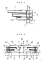
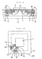
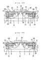
- FIGS. 1 to 10 An example of a printed wiring board in an embodiment mode in the present invention will be explained next by using FIGS. 1 to 10.
- the printed wiring board 100 in this example has a circuit substrate 6 having a conductor circuit 5 and a through hole 60, and a joining pin 1 inserted into the through hole 60.
- the joining pin 1 is manufactured by using a material unmelted at a heating temperature when the joining pin 1 is soldered and joined to an opposite party pad 81 on a mother board 8.
- the joining pin 1 is manufactured by using covar, phosphor bronze, etc.
- the joining pin 1 is constructed by a joining head portion 11 and a leg portion 12.
- the joining head portion 11 is greater than an opening diameter of the through hole 60 and forms a joining portion to the opposite party pad 81.
- the leg portion 12 has a size capable of inserting this leg portion 12 into the through hole 60.
- the leg portion 12 is inserted into the through hole 60 and is joined to a wall face of the through hole 60 by a soldering material 20.
- solder 2 which has a thickness of 10 ⁇ m.
- the joining head portion 11 is formed in the shape of a spherical body having 0. 75 mm in diameter and 0. 6 mm in height.
- a lower portion 111 of the joining head portion 11, i.e., a portion opposed to the circuit substrate 6 in the joining head portion 11 forms a flat face.
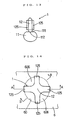
- a central portion 122 of the leg portion 12 is smaller than an end tip portion 121 of the leg portion 12.
- a maximum diameter of the end tip portion 121 of the leg portion 12 is set to 0. 35 mm.
- a minimum diameter of the central portion 122 of the leg portion 12 is set to 0. 2 mm.
- the leg portion 12 has a length of 1.6 mm.
- An opening diameter of the through hole 60 is set to 0. 32 mm.
- the through hole 60 has a length of 1. 8 mm.
- the circuit substrate 6 is formed by laminating and press-attaching through an adhesive 43 plural resin substrates 61 to each other. A surface of each resin substrate 61 is covered with a resist film 69. A concave mounting portion 7 for mounting an electronic part 70 is formed in the circuit substrate 6. A bottom face of the mounting portion 7 is formed by a heat radiating plate 4 adhered to the circuit substrate 6. The heat radiating plate 4 is adhered to the circuit substrate 6 by an adhesive 41.
- the conductor circuit 5 is arranged on a surface of the circuit substrate 6 and is also arranged within this circuit substrate 6.
- the conductor circuit 5 has a bonding pad portion 51 in the vicinity of the mounting portion 7.
- a bonding wire 71 connected to the electronic part 70 is joined to the bonding pad portion 51 by solder.
- the printed wiring board 100 in this example is a substrate of a face-down type for mounting electronic parts.
- the mounting portion 7 for mounting the electronic part 70 is located opposite to the mother board 8.
- the circuit substrate 6 is formed (FIG. 3), the joining pin 1 is inserted (FIG. 5), and the joining pin 1 is joined by the soldering material 20 (FIG. 6).
- a manufacturing method of the printed wiring board will be next explained in detail.
- a copper foil is stuck to plural resin substrates and a through hole for forming a mounting portion is bored.
- the copper foil is etched and a conductor circuit 5 is formed on a surface of each resin substrate 61 as shown in FIG. 3.
- the conductor circuit 5 is also formed by a plating method in the inner wall of a through hole 79.
- each resin substrate 61 is covered with a resist film 69 except for the through hole 79 and a portion near a through hole forming portion. Following this, these resin substrates 61 are laminated and thermally press-attached to each other through an epoxy-system adhesive 43. Thus, a circuit substrate 6 having the multilayer conductor circuit 5 is obtained.
- a through hole 60 extending through the circuit substrate 6 is bored.
- a metallic plating film 600 constructed by copper is formed on a wall face of the through hole 60 by an electroless plating method and an electrolytic plating method.
- the above-mentioned joining pin 1 is press-fitted into the through hole 60 from one opening portion 601 of this through hole 60.
- a surface of the joining pin 1 is covered with solder 2.
- the joining pin 1 is inserted into the through hole 60 while the joining pin 1 presses against a wall face of the through hole 60.
- a lower face 111 of a joining head portion 11 is engaged with an opening portion 601 of the through hole 60 so that the insertion of the joining pin 1 is stopped.
- a soldering material 20 formed in a paste shape is arranged on an opening portion 602 of the through hole 60 on a side opposed to an inserting direction of the joining pin 1.
- the soldering material 20 is melted by IR reflow, hot air reflow methods, etc. so that the interior of the through hole 60 is filled with the soldering material 20.
- the leg portion 12 of the joining pin 1 is joined to the through hole 60 by the soldering material 20.
- a heat radiating plate 4 is adhered to the circuit substrate 6 by an adhesive 41 constructed of epoxy resin.
- the heat radiating plate 4 is adhered to the circuit substrate 6 so as to cover an opening portion of the through hole 79 formed in an outermost resin substrate 61.
- an adhesive 42 constructed of solder there is also a case in which a side face of the heat radiating plate 4 and a surface of the circuit substrate 6 are joined to each other by an adhesive 42 constructed of solder.
- the above printed wiring board 100 is thus obtained.
- an electronic part 70 is adhered to a mounting portion 7 of the above printed wiring board 100 by an adhesive 44.
- the electronic part 70 is electrically connected to a bonding pad portion 51 of the conductor circuit 5 by a bonding wire 71.
- the electronic part 70 and the bonding wire 71 are sealed by resin.
- the joining pin 1 of the printed wiring board 100 is arranged on the surface of an opposite party pad 81 on the mother board 8.
- the solder 2 covering the joining pin 1 is melted by heating the joining pin 1.
- the joining head portion 11 of the joining pin 1 and the opposite party pad 81 are joined to each other by the solder 2.
- the joining pin 1 is inserted into the through hole 60 in the printed wiring board 100.
- the joining pin 1 has the joining head portion 11 for joining the joining pin 1 to the opposite party pad 81.
- the through hole 60 and the opposite party pad 81 can be connected to each other electrically by the joining pin 1 from joining the joining head portion 11 to the opposite party pad 81.
- the through hole 60 and the opposite party pad 81 can be connected to each other by the joining pin 1 in a facing state, it is unnecessary to arrange a pad for mounting a soldering ball in addition to the through hole 60 as in the conventional case. It is also unnecessary to form a conductor circuit for connecting the through hole 60 and the pad for mounting the ball to each other as in the conventional case. Therefore, as shown in FIG. 10, a surplus space is formed on the surface of the circuit substrate 6 in a portion except for the opening portion of the through hole 60. Another conductor circuit 50 can be formed in this space so that a high density wiring structure can be realized.
- the mounting portion 7 is opened on a side opposed to the mother board 8, i. e., a projecting side of the joining pin 1.
- many bonding pad portions 51 are arranged in the vicinity of an opening portion of the mount ing port ion 7. Accordingly, it is necessary to form many conductor circuits 50 to each other for connecting the bonding pad portions 51 and the through hole 60. Therefore, when many conductor circuits 50 are formed in the above surplus space on the surface of the circuit substrate 6 as in this example, the bonding pad portions 51 and the through hole 60 can be connected and wired at high density.
- the printed wiring board 100 of a face-down type as in this example, it is very significant to have a structure in which the joining pin 1 is inserted into the through hole 60 and is joined to the mother board 8 by the joining head portion 11 of the joining pin 1.
- the joining pin 1 is manufactured by using a material unmelted at a heating temperature at which the joining pin 1 is soldered and joined to the opposite party pad 81. Therefore, a constant height of the joining head portion 11 is maintained in the soldering and joining without melting deformation. Accordingly, the joining head portion 11 functions as a strut of the printed wiring board at the soldering and joining times.
- such a joining head portion 11 functioning as a strut is greater than an opening diameter of the through hole 60. Therefore, when the leg portion 12 of the joining pin 1 is inserted into the through hole 60, the joining head portion 11 is engaged with the opening portion 601 of the through hole 60 and does not enter the interior of the through hole 60. Accordingly, the joining head portion 11 can project by the same height from the surface of the circuit substrate 6.
- the joining head portion 11 and the opposite party pad 81 is soldered and joined to each other, the distance between the mother board 8 and the printed wiring board 100 is secured constantly by the joining head portion 11. Accordingly, the printed wiring board 100 can be joined to the mother board 8 arranged in a parallel state.
- the leg portion 12 of the joining pin 1 is inserted into the through hole 60, and the leg portion 12 and the through hole 60 are joined to each other by the soldering material 20. Therefore, in the printed wiring board 100 in this example, it is possible to avoid a structure (see FIG. 29) for joining a soldering ball to a pad for mounting the ball as in the conventional example. Accordingly, there is no apprehension that an intermediate layer is formed between the soldering ball and the pad for mounting the ball. Hence, the joining pin 1 can be strongly fixed to the through hole 60.
- the end tip portion 121 of the leg portion 12 of the joining pin 1 is slightly greater than a diameter of the through hole 60. Therefore, the leg portion 12 is inserted into the through hole 60 while the leg portion 12 presses against a wall face of the through hole 60 and distorts this wall face. Accordingly, the joining pin 1 is fixed to the through hole 60 and does not fall off before solder fills the through hole 60. Further, a filling operation of the soldering material 20 can be performed easily.
- a groove 112 for extracting the air is formed in a lower portion 111 of the joining head portion 11 of the joining pin 1.
- each of the grooves 112 has 0.1 mm inwidth and 0. 05 mm in depth.
- a surface of the joining pin in this example is covered with unillustrated solder.
- the interior of the through hole 60 is filled with the soldering material 20 from an opening portion 602 on a side opposed to an inserting direction of the joining pin 1.
- the interior of the through hole 60 can also be filled with the soldering material 20 from the opening portion 601 in a reverse direction, i.e., on the same side as the inserting direction of the joining pin 1.
- the interior of the through hole 60 filled with the soldering material 20 by a method for dipping the above circuit substrate into a melting solder reservoir.
- a leg portion 12 of the joining pin 1 has plural projecting portions 125 widened in a radiating shape.
- Each of the projecting portions 125 has a maximum diameter of 0. 35 mm slightly greater than a diameter of the through hole 60.
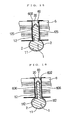
- a groove 112 is formed in a joining head portion 11 of the joining pin 1. As shown in FIGS. 15 and 16, a surface of the joining pin 1 is covered with solder 2.
- the other constructions are similar to those in the embodiment mode example 1.
- the plural projecting portions 125 are formed in the leg portion 12 of the joining pin 1. Therefore, as shown in FIGS. 15 and 16, when each projecting portion 125 is inserted into the through hole 60, both ends of the projecting portion 125 are inserted into the through hole 60 while both the ends of the projecting portion 125 locally press against a wall face of the through hole 60, since the projecting portion 125 is slightly greater than the diameter of the through hole 60. Therefore, it is possible to insert the joining pin 1 by small pressing force in comparison with the joining pin 1 in the embodiment mode example 1 in which an entire inner wall of the through hole 60 is pressed.
- a mel ted soldering material 20 is flowed from an opening portion 602 on a side opposed to the inserting direction of the joining pin 1, and fills the interior of the through hole 60.
- the air existing within the through hole 60 is discharged outward through a clearance 606 between the through hole 60 and the leg portion 12 of the joining pin 1, and the groove 112. Therefore, the interior of the through hole 60 can be filled with the soldering material 20 without sealing the air.
- a concave mounting portion 7 for mounting an electronic part 70 constitutes a substrate of a face-up type for mounting electronic parts and opened on a side opposed to a mother board 8.
- a joining head portion 11 of the joining pin 1 projects from the through hole 60 on a side opposed to the mother board 8 in the circuit substrate 6.
- surface high density wiring of the circuit substrate 6 can be performed and the printed wiring board can be joined to the mother board 8 in parallel with this mother board 8 and is superior in joining strength.
- FIGS. 18 to 24 A printed wiring board in an embodiment mode example will be explained by using FIGS. 18 to 24.
- the printed wiring board 100 in this example has a circuit substrate 6 having a conductor circuit 5 and a through hole 60, and a joining ball 3 joined to the through hole 60.
- the joining ball 3 is manufactured by using a material unmelted at a heating temperature when the joining ball 3 is soldered and joined to an opposite party pad 81 on a mother board 8.
- the joining ball 3 is manufactured by using covar, phosphor bronze, etc.
- the joining ball 3 is constructed by a joining head portion 31 and a bottom portion 32.
- the joining head portion 31 is greater than the diameter of an opening portion 601 of the through hole 60 and forms a joining portion to the opposite party pad 81.
- the bottom portion 32 is opposed to the opening portion 601 of the through hole 60.
- the bottom portion 32 is arranged in the opening portion 601 of the through hole 60 and is joined to the through hole 60 by a soldering material 20 filling the interior of the through hole 60.
- the joining head portion 31 and the bottom portion 32 of the joining ball 3 are covered with solder 2 having 0. 01 to 0. 015 mm in thickness.
- the joining head portion 31 of the joining ball 3 is formed in the shape of a spherical body having 0. 75 mm in diameter.
- the bottom portion 32 is formed in a flat face shape and a circular shape having 0. 6 mm in diameter.
- the opening portion 601 of the through hole 60 has 0. 32 mm in diameter.
- a multilayer circuit substrate 6 having a through hole 60 is formed first (see FIGS. 3 and 4).
- a joining ball 3 is arranged on a flat face base 390.
- a bottom portion 32 of the joining ball 3 is set to face the flat face base 390 by slightly vibrating the flat face base 390, and a joining head portion 31 is directed upward.
- the joining head portion 31 of the joining ball 3 is absorbed and held by a sucking port 391 of a sucking device 39 by making the sucking port 391 approach the flat face base 390.
- the sucking device 39 is moved above the above circuit substrate 6 while the sucking device 39 absorbs and holds the joining ball 3. Positions of the joining ball 3 and the through hole 60 are aligned with each other.
- the sucking device 39 is set to approach the circuit substrate 6 and the joining ball 3 is arranged in the opening portion 601 of the through hole 60 which is arranged in the circuit substrate 6. At this time, since the joining head portion 31 of the joining ball 3 is absorbed and held in the sucking port 391, the bottom portion 32 of the joining ball 3 faces the opening portion 601.
- the interior of the through hole 60 is filled with a soldering material 20 from an opening portion 602 on an unarranged side of the joining ball 3 in a fixing state of the sucking device 39 and the circuit substrate 6.
- the interior of the through hole 60 is filled with the soldering material 20 by a method for dipping the circuit substrate into a soldering bath, a method for applying a supersonic wave to the soldering bath dipping the circuit substrate thereinto, etc.
- the soldering material 20 is cooled, solidified and congealed.
- the joining ball 3 is joined to the through hole 60 by the soldering material 20.
- the sucking port 391 is detached from the joining ball 3 by weakening the sucking force of the sucking device 39.
- a heat radiating plate 4 is adhered to the circuit substrate 6 by an adhesive 41 constructed by epoxy resin.
- the heat radiating plate 4 is adhered to the circuit substrate 6 so as to cover an opening portion of a through hole 79 formed in an outermost resin substrate 61.
- an adhesive 42 constructed by solder there is also a case in which a side face of the heat radiating plate 4 and a surface of the circuit substrate 6 are joined to each other by an adhesive 42 constructed by solder.
- an electronic part 70 is adhered to a mounting portion 7 by an adhesive 44 in the above printed wiring board 100.
- the electronic part 70 and a bonding pad portion 51 of a conductor circuit 5 are electrically connected to each other by a bonding wire 71.
- the electronic part 70 and the bonding wire 71 are then sealed by resin.
- the joining ball 3 of the printed wiring board 100 is arranged on the surface of an opposite party pad 81 on a mother board 8.
- solder 2 covering the joining ball 3 is melted by heating this joining ball 3.
- the joining head portion 31 of the joining ball 3 and the opposite party pad 81 are joined to each other by the solder 2.
- the joining ball 3 is joined to the through hole 60.
- the joining ball 3 has the joining head portion 31 for joining the joining ball 3 to the opposite party pad 81. Therefore, the through hole 60 and the opposite party pad 81 can be electrically connected to each other by the joining ball 3 by joining the joining head portion 31 to the opposite party pad 81.
- the joining ball 3 is joined to the opening portion 601 of the through hole 60. Therefore, the through hole 60 and the opposite party pad 81 can be electrically connected to each other in a facing state. Accordingly, it is unnecessary to arrange a pad for mounting a soldering ball in addition to the through hole 60 as in the conventional case. It is also unnecessary to form a conductor circuit for connecting the through hole 60 and the pad for mounting the ball as in the conventional case. Therefore, a surplus space is formed on a surface of the circuit substrate 6 in a portion except for the through hole 60 (see FIG. 10). Another conductor circuit 50 can be formed in this space so that a high density wiring structure can be realized.
- the printed wiring board 100 particularly in this example is of a face-down type as shown in FIG. 24. Therefore, a structure for fixedly joining the joining ball 3 to the through hole 60 and joining the printed wiring board 100 to the mother board 8 by the joining head portion 31 of the joining ball 3 is extremely significant to produce high density wiring between plural bonding pad portions 51 and the through hole 60.
- the joining ball 3 is manufactured by using a material unmelted at a heating temperature when the joining ball 3 is soldered and joined to the opposite party pad 81. Therefore, a constant height of the joining ball 3 is maintained without melting deformation in the soldering and joining. Accordingly, the joining ball 3 functions as a strut of the printed wiring board 100 at the soldering and joining times.
- the joining head portion 31 of such a joining ball 3 is greater than the opening portion 601 of the through hole 60 functioning as a strut. Therefore, when the joining ball 3 is joined to the through hole 60, the joining head portion 31 is engaged with the opening portion 601 of the through hole 60 and does not enter the interior of the through hole 60. Accordingly, the joining head portion 31 can project by the same height from the surface of the circuit substrate 6.
- the joining head portion 31 and the opposite party pad 81 are soldered and joined to each other, the distance between the mother board 8 and the printed wiring board 100 is constantly secured by the joining head portion 31. Accordingly, the printed wiring board 100 can be joined to the mother board 8 in a parallel arranging state.
- the bottom portion 32 of the joining ball 3 is joined to the opening portion 601 of the through hole 60 by the soldering material 20. Therefore, similar to the embodiment mode example 1, there is no apprehension of an intermediate layer forming causing a reduction in joining strength. Accordingly, the joining ball 3 can be strongly fixed to the through hole 60.
- a bottom portion 321 of the joining ball 3 constitutes one portion of a spherical surface.
- an entire shape of the joining ball 3 including the joining head portion 31 and the bottom portion 321 is formed as a spherical body which has a diameter of 0. 75 mm. Therefore, a joining area of an inner wall of the through hole 60 and a soldering material 20 is increased. Accordingly, the joining ball 3 is more reliably joined to the through hole 60.
- the other constructions are similar to those in the embodiment mode example 5, and similar effects can be obtained to those in the embodiment mode example 5.
- a printed wiring board 100 in this example is a substrate of a face-up type for mounting electronic parts in which a concave mounting portion 7 for mounting an electronic part 70 is opened on a side opposed to a mother board 8.
- a joining head portion 31 of the joining ball 3 projects from the through hole 60 on a side opposed to the mother board 8 in the circuit substrate 6.
- high density wiring can be performed on a surface of the circuit substrate and the printed wiring board can be joined to the mother board parallel with the mother board which has a superior joining strength.
- the present invention can provide a printed wiring board and its manufacturing method in which high density wiring can be performed on a substrate surface and the printed wiring board can be joined to a partner member in parallel with the partner member which has a superior joining strength.
Landscapes
- Engineering & Computer Science (AREA)
- Manufacturing & Machinery (AREA)
- Microelectronics & Electronic Packaging (AREA)
- Combinations Of Printed Boards (AREA)
- Multi-Conductor Connections (AREA)
- Printing Elements For Providing Electric Connections Between Printed Circuits (AREA)
- Coupling Device And Connection With Printed Circuit (AREA)
- Electric Connection Of Electric Components To Printed Circuits (AREA)
- Production Of Multi-Layered Print Wiring Board (AREA)
Abstract
Claims (9)
- Carte de câblage imprimée (100) ayant un substrat de circuit (6) ayant un circuit conducteur (5) et un trou d'insertion (60), et une broche de raccordement (1) insérée dans ledit trou d'insertion (60) ;
ladite broche de raccordement (1) étant construite par une partie de tête de raccordement (11) plus grande qu'un diamètre d'ouverture dudit trou d'insertion (60) et formant une partie de raccordement pour joindre une pastille opposée, et une partie de patte (12) ayant une taille permettant d'insérer cette partie de patte (12) dans ledit trou d'insertion, la partie de patte étant insérée dans ledit trou d'insertion (60) et étant raccordée au trou d'insertion (60) par un matériau conducteur ;
la carte de câblage imprimée (100) étant caractérisée en ce que ladite broche de raccordement (1) est fabriquée en utilisant un matériau n'étant pas fondu à une température de chauffage convenant pour joindre la broche de raccordement (1) à une pastille opposée et ladite broche de raccordement (1) a une partie centrale (122) plus petite qu'une partie d'extrémité (121) de la partie de patte (12),
ladite partie de patte (12) ayant des parties saillantes (125) faisant saillie dans plusieurs directions de telle manière qu'un espace ayant une forme en coupe ondulée est formé,
et ledit espace de forme ondulée en section transversale et la partie centrale (122) de la partie de patte (12) sont remplies avec un matériau conducteur. - Carte de câblage imprimée selon la revendication 1, dans laquelle la partie de tête de raccordement de ladite broche de raccordement est couverte avec le matériau conducteur.
- Carte de câblage imprimée selon la revendication 1 ou 2, dans laquelle ladite partie de tête de raccordement (11) est construite par un corps sphérique.
- Procédé de fabrication d'une carte- de câblage imprimée caractérisé en ce que le procédé de fabrication comprend :un process pour préparer un substrat de circuit ayant un circuit conducteur et un trou d'insertion ;un process pour fabriquer une broche de raccordement formée par un matériau ne fondant pas à une température de chauffage convenable pour joindre la broche de raccordement à une pastille opposée, et construite par une partie de patte, ladite partie de patte (12) ayant des parties saillantes (125) faisant saillie dans plusieurs directions de telle manière qu'un espace ayant une forme ondulée en section transversale est formé, une partie centrale (122) plus petite qu'une partie d'extrémité (121) de la partie de patte (12), et une partie de tête de raccordement (11) plus grande qu'un diamètre d'ouverture dudit trou d'insertion et formant une partie de raccordement pour joindre à la pastille opposée ;un process pour insérer la partie de patte de ladite broche de raccordement dans ledit trou d'insertion ; etun process pour remplir ledit espace ayant une forme ondulée en section transversale et la partie centrale (122) de la partie de patte (12) dans ledit trou d'insertion avec un matériau conducteur et raccorder ledit trou d'insertion et ladite partie de patte ensemble par le matériau conducteur.
- Procédé de fabrication de la carte de câblage imprimée selon la revendication 4, dans lequel la partie de tête de raccordement de ladite broche de raccordement est couverte avec le matériau conducteur à l'avance avant que la partie de tête de raccordement soit insérée dans le trou d'insertion.
- Carte de câblage imprimée selon l'une quelconque des revendications 1 à 3, dans laquelle ledit matériau conducteur est un matériau de soudure.
- Carte de câblage imprimée selon l'une quelconque des revendications 1 à 3, dans laquelle ledit matériau conducteur est une résine époxy imprégnée avec une charge d'argent.
- Procédé de fabrication d'une carte de câblage imprimée selon la revendication 4 ou 5, dans laquelle ledit matériau conducteur est un matériau de soudure.
- Procédé de fabrication d'une carte de câblage imprimée selon la revendication 4 ou 5, dans laquelle ledit matériau conducteur est une résine époxy imprégnée avec une charge d'argent.
Priority Applications (1)
| Application Number | Priority Date | Filing Date | Title |
|---|---|---|---|
| EP07100813A EP1776001B1 (fr) | 1997-01-30 | 1998-01-05 | Panneau à circuit imprimé et son procédé de fabrication |
Applications Claiming Priority (8)
| Application Number | Priority Date | Filing Date | Title |
|---|---|---|---|
| JP3303397 | 1997-01-30 | ||
| JP3303397 | 1997-01-30 | ||
| JP3303497 | 1997-01-30 | ||
| JP3303497 | 1997-01-30 | ||
| JP9340723A JPH10275966A (ja) | 1997-01-30 | 1997-11-25 | プリント配線板及びその製造方法 |
| JP34072397 | 1997-11-25 | ||
| PCT/JP1998/000006 WO1998034443A1 (fr) | 1997-01-30 | 1998-01-05 | Carte imprimee et son procede de production |
| US09/359,981 US6444924B1 (en) | 1997-01-30 | 1999-07-23 | Printed wiring board with joining pin and manufacturing method therefor |
Related Child Applications (1)
| Application Number | Title | Priority Date | Filing Date |
|---|---|---|---|
| EP07100813A Division EP1776001B1 (fr) | 1997-01-30 | 1998-01-05 | Panneau à circuit imprimé et son procédé de fabrication |
Publications (3)
| Publication Number | Publication Date |
|---|---|
| EP0959648A1 EP0959648A1 (fr) | 1999-11-24 |
| EP0959648A4 EP0959648A4 (fr) | 2004-06-23 |
| EP0959648B1 true EP0959648B1 (fr) | 2007-03-14 |
Family
ID=27459728
Family Applications (1)
| Application Number | Title | Priority Date | Filing Date |
|---|---|---|---|
| EP98900160A Expired - Lifetime EP0959648B1 (fr) | 1997-01-30 | 1998-01-05 | Carte imprimee et son procede de production |
Country Status (4)
| Country | Link |
|---|---|
| US (3) | US6444924B1 (fr) |
| EP (1) | EP0959648B1 (fr) |
| JP (1) | JPH10275966A (fr) |
| WO (1) | WO1998034443A1 (fr) |
Families Citing this family (32)
| Publication number | Priority date | Publication date | Assignee | Title |
|---|---|---|---|---|
| JPH10275966A (ja) | 1997-01-30 | 1998-10-13 | Ibiden Co Ltd | プリント配線板及びその製造方法 |
| US6208022B1 (en) | 1997-03-27 | 2001-03-27 | Nec Corporation | Electronic-circuit assembly |
| KR100393271B1 (ko) * | 1997-11-19 | 2003-07-31 | 이비덴 가부시키가이샤 | 다층 전자부품탑재용 기판의 제조 방법 |
| WO2002027792A2 (fr) * | 2000-09-27 | 2002-04-04 | Conexant Systems, Inc. | Boitiers de puces a liaison par fils a faible induction |
| JP4744689B2 (ja) * | 2000-12-11 | 2011-08-10 | パナソニック株式会社 | 粘性流体転写装置及び電子部品実装装置 |
| JP3527229B2 (ja) | 2002-05-20 | 2004-05-17 | 沖電気工業株式会社 | 半導体装置、半導体装置の実装方法、及び半導体装置のリペア方法 |
| JP4363823B2 (ja) * | 2002-07-04 | 2009-11-11 | 富士通マイクロエレクトロニクス株式会社 | 半導体装置の実装システム |
| US6828512B2 (en) * | 2002-10-08 | 2004-12-07 | Intel Corporation | Apparatus and methods for interconnecting components to via-in-pad interconnects |
| JP2005150263A (ja) * | 2003-11-13 | 2005-06-09 | Nitto Denko Corp | 両面配線回路基板 |
| US20050195528A1 (en) * | 2004-03-05 | 2005-09-08 | Bennin Jeffry S. | Coined ground features for integrated lead suspensions |
| US7375288B1 (en) * | 2004-07-30 | 2008-05-20 | Intel Corp. | Apparatuses and methods for improving ball-grid-array solder joint reliability |
| JP5011765B2 (ja) * | 2005-03-15 | 2012-08-29 | 富士ゼロックス株式会社 | 液滴吐出ヘッド及び液滴吐出装置 |
| KR100725517B1 (ko) * | 2005-08-08 | 2007-06-07 | 삼성전자주식회사 | 본딩 패드와 볼 랜드가 복수 층에 형성된 다층 배선 기판및 이를 이용한 반도체 패키지 구조 |
| JP2007335675A (ja) * | 2006-06-15 | 2007-12-27 | Fuji Electric Systems Co Ltd | 電源装置および電源装置の製造方法 |
| JP5050638B2 (ja) * | 2007-05-11 | 2012-10-17 | ブラザー工業株式会社 | 液滴吐出装置 |
| JP2009032417A (ja) * | 2007-07-24 | 2009-02-12 | Nissha Printing Co Ltd | タッチ入力機能付きの保護パネルとその製造方法 |
| US8378231B2 (en) * | 2008-07-31 | 2013-02-19 | Ibiden Co., Ltd. | Semiconductor device and method for manufacturing the same |
| US8529081B2 (en) | 2010-04-23 | 2013-09-10 | Surefire, Llc | Headlamp device with housing providing thermal management |
| US8395058B2 (en) * | 2010-04-23 | 2013-03-12 | Surefire, Llc | Metal core circuit board with conductive pins |
| CN102469686A (zh) * | 2010-11-16 | 2012-05-23 | 欣兴电子股份有限公司 | 电路板结构及其制作方法 |
| JP5686009B2 (ja) | 2011-03-18 | 2015-03-18 | 富士通株式会社 | 基板ユニット、及び、基板ユニットの製造方法 |
| US10138114B2 (en) * | 2011-08-03 | 2018-11-27 | Product Spring, Llc | Powder dispensing apparatus |
| ITMI20112084A1 (it) * | 2011-11-17 | 2013-05-18 | St Microelectronics Srl | Saldatura ad onda su scheda a circuito stampato di dispositivi elettronici a montaggio superficiale |
| US20130208424A1 (en) * | 2012-02-14 | 2013-08-15 | Robert W. Warren | Solid via pins for improved thermal and electrical conductivity |
| JP2014192177A (ja) * | 2013-03-26 | 2014-10-06 | Ngk Spark Plug Co Ltd | 配線基板 |
| JP6151572B2 (ja) * | 2013-05-30 | 2017-06-21 | 京セラ株式会社 | 電子素子搭載用基板および電子装置 |
| US9679865B2 (en) * | 2013-11-08 | 2017-06-13 | SK Hynix Inc. | Substrate for semiconductor package and semiconductor package having the same |
| IT201700073501A1 (it) * | 2017-06-30 | 2018-12-30 | St Microelectronics Srl | Prodotto a semiconduttore e corrispondente procedimento |
| CN111987084B (zh) * | 2019-05-24 | 2022-07-26 | 方略电子股份有限公司 | 电子装置及其制造方法 |
| US11676932B2 (en) * | 2019-12-31 | 2023-06-13 | Micron Technology, Inc. | Semiconductor interconnect structures with narrowed portions, and associated systems and methods |
| DE102023125592B4 (de) | 2023-09-21 | 2025-05-28 | Infineon Technologies Ag | Laminatträger mit eingebettetem elektronischem Bauteil, das mit einem hervorstehenden Stift elektrisch gekoppelt ist |
| US20250227837A1 (en) * | 2024-01-09 | 2025-07-10 | Rockwell Collins, Inc. | Selective removal of adhesive from coverlay for printed circuit board insulation |
Family Cites Families (62)
| Publication number | Priority date | Publication date | Assignee | Title |
|---|---|---|---|---|
| FR2571547B1 (fr) * | 1984-10-05 | 1987-07-24 | Thomson Csf | Circuit hybride reportable sur un support comportant un reseau d'interconnexion a haute densite |
| US4700276A (en) * | 1986-01-03 | 1987-10-13 | Motorola Inc. | Ultra high density pad array chip carrier |
| JPS62164897A (ja) | 1986-01-14 | 1987-07-21 | Tanaka Kikinzoku Kogyo Kk | 導電用複合ブスバ− |
| JPS62241361A (ja) * | 1986-04-14 | 1987-10-22 | Hitachi Ltd | 半導体装置 |
| JPS62244156A (ja) * | 1986-04-16 | 1987-10-24 | Ibiden Co Ltd | 表面実装用パツケ−ジ |
| EP0263222B1 (fr) * | 1986-10-08 | 1992-03-25 | International Business Machines Corporation | Procédé pour la formation de bornes de brasure pour un module en céramique sans broches |
| JP2806928B2 (ja) | 1987-05-29 | 1998-09-30 | 大日本印刷株式会社 | 感光性樹脂層の形成法 |
| JPS648649U (fr) | 1987-07-07 | 1989-01-18 | ||
| JP2613769B2 (ja) | 1987-09-02 | 1997-05-28 | 有限会社エム・エス・ケー | 繊維製品の処理法 |
| JPH0161572U (fr) | 1987-10-05 | 1989-04-19 | ||
| US4861944A (en) * | 1987-12-09 | 1989-08-29 | Cabot Electronics Ceramics, Inc. | Low cost, hermetic pin grid array package |
| JP2898985B2 (ja) | 1988-03-14 | 1999-06-02 | キヤノン株式会社 | 画像処理方法 |
| JPH02144945A (ja) * | 1988-11-28 | 1990-06-04 | Sumitomo Bakelite Co Ltd | 半導体搭載用基板およびその製造方法 |
| JPH02102738U (fr) * | 1989-01-31 | 1990-08-15 | ||
| JPH02239577A (ja) * | 1989-03-14 | 1990-09-21 | Nec Corp | 表面実装用混成集積回路 |
| JPH0785599B2 (ja) | 1989-04-28 | 1995-09-13 | 日本電気株式会社 | リモコン送信用集積回路 |
| JP2717313B2 (ja) | 1989-09-07 | 1998-02-18 | イビデン株式会社 | 電子部品搭載用基板の製造方法 |
| JP2791995B2 (ja) * | 1989-10-31 | 1998-08-27 | イビデン株式会社 | プリント配線板 |
| JPH03190063A (ja) * | 1989-12-19 | 1991-08-20 | Matsushita Electric Works Ltd | 半導体チップキャリア用端子ピン |
| JP2536274B2 (ja) | 1990-10-25 | 1996-09-18 | 日本電気株式会社 | ポリイミド多層配線基板の製造方法 |
| US5129142A (en) * | 1990-10-30 | 1992-07-14 | International Business Machines Corporation | Encapsulated circuitized power core alignment and lamination |
| JPH05111596A (ja) | 1991-10-24 | 1993-05-07 | Sharp Corp | 洗濯機 |
| JPH05183019A (ja) * | 1991-12-27 | 1993-07-23 | Hitachi Ltd | 半導体装置およびその製造方法 |
| JPH05206601A (ja) * | 1992-01-28 | 1993-08-13 | Fujitsu Isotec Ltd | プリント基板及びそのアース方法 |
| JPH067252A (ja) | 1992-06-29 | 1994-01-18 | Nitto Kohki Co Ltd | 抽出装置の洗浄方法および洗浄剤包装体 |
| JPH0645722A (ja) * | 1992-07-24 | 1994-02-18 | Ibiden Co Ltd | ピン立て型プリント回路基板 |
| US5497546A (en) * | 1992-09-21 | 1996-03-12 | Matsushita Electric Works, Ltd. | Method for mounting lead terminals to circuit board |
| JP3267704B2 (ja) | 1992-11-27 | 2002-03-25 | 東芝プラント建設株式会社 | 水中溶存酸素の除去方法 |
| US5450290A (en) * | 1993-02-01 | 1995-09-12 | International Business Machines Corporation | Printed circuit board with aligned connections and method of making same |
| US5291062A (en) * | 1993-03-01 | 1994-03-01 | Motorola, Inc. | Area array semiconductor device having a lid with functional contacts |
| JPH06326438A (ja) | 1993-05-13 | 1994-11-25 | Nitto Denko Corp | 単層配線ユニットおよび多層回路配線板ならびにその製法 |
| JPH0714942A (ja) * | 1993-06-15 | 1995-01-17 | Shinko Electric Ind Co Ltd | 半導体装置 |
| JPH0738245A (ja) | 1993-07-23 | 1995-02-07 | Toyota Motor Corp | 電子部品の実装方法 |
| JPH07238022A (ja) | 1994-02-28 | 1995-09-12 | Sanwa Kagaku Kenkyusho Co Ltd | インターフェロン作用効果増強剤 |
| US5367435A (en) * | 1993-11-16 | 1994-11-22 | International Business Machines Corporation | Electronic package structure and method of making same |
| US5435480A (en) * | 1993-12-23 | 1995-07-25 | International Business Machines Corporation | Method for filling plated through holes |
| JP2891085B2 (ja) | 1994-01-26 | 1999-05-17 | 松下電工株式会社 | 半田ボール電極形成方法及びその半田ボール電極形成方法に用いる半田微細球位置決め治具 |
| FR2722916A1 (fr) * | 1994-02-22 | 1996-01-26 | Nec Corp | Element de connexion et procede de connexion mettant en oeuvre cet element |
| JP3166490B2 (ja) | 1994-07-06 | 2001-05-14 | 日立電線株式会社 | Bga型半導体装置 |
| AT401704B (de) * | 1995-01-11 | 1996-11-25 | Mikroelektronik Ges Mit Beschr | Trägerplatte für integrierte schaltkreise |
| JPH08213748A (ja) * | 1995-01-31 | 1996-08-20 | Mitsui High Tec Inc | 基板およびその製造方法 |
| JP2636779B2 (ja) | 1995-02-27 | 1997-07-30 | 日本電気株式会社 | ボール状外部接続端子の構造およびその形成方法 |
| JP3250414B2 (ja) | 1995-03-29 | 2002-01-28 | 三菱マテリアル株式会社 | チタンの炭窒酸化物層表面被覆切削工具の製造方法 |
| JP2735045B2 (ja) * | 1995-09-18 | 1998-04-02 | 日本電気株式会社 | 半導体装置およびその製造方法 |
| JP3843514B2 (ja) * | 1995-12-15 | 2006-11-08 | イビデン株式会社 | 電子部品搭載用基板及びその製造方法 |
| US5973396A (en) * | 1996-02-16 | 1999-10-26 | Micron Technology, Inc. | Surface mount IC using silicon vias in an area array format or same size as die array |
| KR100268632B1 (ko) * | 1996-03-08 | 2000-10-16 | 야마구치 다케시 | 범프형성방법 및 장치 |
| JP3004931B2 (ja) * | 1996-03-28 | 2000-01-31 | ホーヤ株式会社 | 半導体接続基板の製造方法、及びベアチップ搭載ボード |
| US5764485A (en) * | 1996-04-19 | 1998-06-09 | Lebaschi; Ali | Multi-layer PCB blockade-via pad-connection |
| JPH10117067A (ja) | 1996-10-11 | 1998-05-06 | Shinko Electric Ind Co Ltd | 多層配線基板及びその製造方法 |
| US5879787A (en) * | 1996-11-08 | 1999-03-09 | W. L. Gore & Associates, Inc. | Method and apparatus for improving wireability in chip modules |
| JPH10275966A (ja) | 1997-01-30 | 1998-10-13 | Ibiden Co Ltd | プリント配線板及びその製造方法 |
| US5952716A (en) * | 1997-04-16 | 1999-09-14 | International Business Machines Corporation | Pin attach structure for an electronic package |
| JPH11102986A (ja) * | 1997-09-25 | 1999-04-13 | Matsushita Electric Works Ltd | 半導体パッケージ |
| US6300678B1 (en) * | 1997-10-03 | 2001-10-09 | Fujitsu Limited | I/O pin having solder dam for connecting substrates |
| US6037044A (en) * | 1998-01-08 | 2000-03-14 | International Business Machines Corporation | Direct deposit thin film single/multi chip module |
| US6013877A (en) * | 1998-03-12 | 2000-01-11 | Lucent Technologies Inc. | Solder bonding printed circuit boards |
| US6595408B1 (en) * | 1998-10-07 | 2003-07-22 | Micron Technology, Inc. | Method of attaching solder balls to BGA package utilizing a tool to pick and dip the solder ball in flux prior to placement |
| JP3160583B2 (ja) * | 1999-01-27 | 2001-04-25 | 日本特殊陶業株式会社 | 樹脂製基板 |
| US6896526B2 (en) * | 1999-12-20 | 2005-05-24 | Synqor, Inc. | Flanged terminal pins for DC/DC converters |
| DE60031448T2 (de) * | 2000-01-13 | 2007-02-01 | Nitto Denko Corp., Ibaraki | Poröse klebefolie, halbleiterwafer mit poröser klebefolie sowie verfahren zu dessen herstellung |
| US6589594B1 (en) * | 2000-08-31 | 2003-07-08 | Micron Technology, Inc. | Method for filling a wafer through-via with a conductive material |
-
1997
- 1997-11-25 JP JP9340723A patent/JPH10275966A/ja active Pending
-
1998
- 1998-01-05 WO PCT/JP1998/000006 patent/WO1998034443A1/fr not_active Ceased
- 1998-01-05 EP EP98900160A patent/EP0959648B1/fr not_active Expired - Lifetime
-
1999
- 1999-07-23 US US09/359,981 patent/US6444924B1/en not_active Expired - Lifetime
-
2002
- 2002-07-15 US US10/195,865 patent/US6784374B2/en not_active Expired - Lifetime
-
2004
- 2004-08-26 US US10/927,413 patent/US7222776B2/en not_active Expired - Fee Related
Also Published As
| Publication number | Publication date |
|---|---|
| US6444924B1 (en) | 2002-09-03 |
| US20020182903A1 (en) | 2002-12-05 |
| JPH10275966A (ja) | 1998-10-13 |
| US7222776B2 (en) | 2007-05-29 |
| US20050023034A1 (en) | 2005-02-03 |
| WO1998034443A1 (fr) | 1998-08-06 |
| EP0959648A1 (fr) | 1999-11-24 |
| EP0959648A4 (fr) | 2004-06-23 |
| US6784374B2 (en) | 2004-08-31 |
Similar Documents
| Publication | Publication Date | Title |
|---|---|---|
| EP0959648B1 (fr) | Carte imprimee et son procede de production | |
| US5438478A (en) | Electronic component carriers and method of producing the same as well as electronic devices | |
| JPH1174651A (ja) | プリント配線板及びその製造方法 | |
| US5914859A (en) | Electronic component mounting base board and method of producing the same | |
| EP1571706A1 (fr) | Dispositif electronique | |
| JP4899269B2 (ja) | 電子部品ユニットおよびその製造方法 | |
| JP2784522B2 (ja) | 電子部品搭載用基板及びその製造法 | |
| KR100386810B1 (ko) | 모듈 기판의 제조방법 | |
| JP2791995B2 (ja) | プリント配線板 | |
| EP1776001B1 (fr) | Panneau à circuit imprimé et son procédé de fabrication | |
| US20030082848A1 (en) | Semiconductor device and manufacturing method | |
| JP3346216B2 (ja) | プリント配線板 | |
| JPH0539464A (ja) | 接着フイルムおよびフイルムキヤリアならびにそれを用いた接続構造 | |
| JP3694949B2 (ja) | 電子部品搭載用基板 | |
| JPS61214548A (ja) | テ−プキヤリア | |
| JPH06334059A (ja) | 半導体搭載用基板及びその製造方法 | |
| JPH10335388A (ja) | ボールグリッドアレイ | |
| JPS62194655A (ja) | 電子装置用接続パツケ−ジ及びその製造方法 | |
| JP3174975B2 (ja) | 電子部品搭載装置 | |
| JP2001291800A (ja) | 電子部品用パッケージ | |
| KR20020057670A (ko) | 반도체 칩 패키지 및 그 제조방법 | |
| JPH1022427A (ja) | 半導体装置用パッケージ及びその製造方法 | |
| JP2003338574A (ja) | ピン付き配線基板およびこれを用いた電子装置 | |
| JP2001332657A (ja) | 半導体パッケージ | |
| JPH10294400A (ja) | 面付実装用電子部品 |
Legal Events
| Date | Code | Title | Description |
|---|---|---|---|
| PUAI | Public reference made under article 153(3) epc to a published international application that has entered the european phase |
Free format text: ORIGINAL CODE: 0009012 |
|
| 17P | Request for examination filed |
Effective date: 19990804 |
|
| AK | Designated contracting states |
Kind code of ref document: A1 Designated state(s): DE GB |
|
| A4 | Supplementary search report drawn up and despatched |
Effective date: 20040512 |
|
| 17Q | First examination report despatched |
Effective date: 20040810 |
|
| GRAP | Despatch of communication of intention to grant a patent |
Free format text: ORIGINAL CODE: EPIDOSNIGR1 |
|
| GRAS | Grant fee paid |
Free format text: ORIGINAL CODE: EPIDOSNIGR3 |
|
| RIN1 | Information on inventor provided before grant (corrected) |
Inventor name: ASANO, KOUJI Inventor name: ISHIDA, NAOTO |
|
| GRAA | (expected) grant |
Free format text: ORIGINAL CODE: 0009210 |
|
| AK | Designated contracting states |
Kind code of ref document: B1 Designated state(s): DE GB |
|
| REG | Reference to a national code |
Ref country code: GB Ref legal event code: FG4D |
|
| REF | Corresponds to: |
Ref document number: 69837319 Country of ref document: DE Date of ref document: 20070426 Kind code of ref document: P |
|
| PLBE | No opposition filed within time limit |
Free format text: ORIGINAL CODE: 0009261 |
|
| STAA | Information on the status of an ep patent application or granted ep patent |
Free format text: STATUS: NO OPPOSITION FILED WITHIN TIME LIMIT |
|
| 26N | No opposition filed |
Effective date: 20071217 |
|
| PGFP | Annual fee paid to national office [announced via postgrant information from national office to epo] |
Ref country code: DE Payment date: 20130103 Year of fee payment: 16 Ref country code: GB Payment date: 20130102 Year of fee payment: 16 |
|
| REG | Reference to a national code |
Ref country code: DE Ref legal event code: R119 Ref document number: 69837319 Country of ref document: DE |
|
| GBPC | Gb: european patent ceased through non-payment of renewal fee |
Effective date: 20140105 |
|
| REG | Reference to a national code |
Ref country code: DE Ref legal event code: R119 Ref document number: 69837319 Country of ref document: DE Effective date: 20140801 |
|
| PG25 | Lapsed in a contracting state [announced via postgrant information from national office to epo] |
Ref country code: DE Free format text: LAPSE BECAUSE OF NON-PAYMENT OF DUE FEES Effective date: 20140801 |
|
| PG25 | Lapsed in a contracting state [announced via postgrant information from national office to epo] |
Ref country code: GB Free format text: LAPSE BECAUSE OF NON-PAYMENT OF DUE FEES Effective date: 20140105 |