EP0991012A1 - Chip-karte - Google Patents
Chip-karte Download PDFInfo
- Publication number
- EP0991012A1 EP0991012A1 EP98900201A EP98900201A EP0991012A1 EP 0991012 A1 EP0991012 A1 EP 0991012A1 EP 98900201 A EP98900201 A EP 98900201A EP 98900201 A EP98900201 A EP 98900201A EP 0991012 A1 EP0991012 A1 EP 0991012A1
- Authority
- EP
- European Patent Office
- Prior art keywords
- data
- card
- response
- memory
- state
- Prior art date
- Legal status (The legal status is an assumption and is not a legal conclusion. Google has not performed a legal analysis and makes no representation as to the accuracy of the status listed.)
- Granted
Links
Images


Classifications
-
- G—PHYSICS
- G06—COMPUTING OR CALCULATING; COUNTING
- G06K—GRAPHICAL DATA READING; PRESENTATION OF DATA; RECORD CARRIERS; HANDLING RECORD CARRIERS
- G06K19/00—Record carriers for use with machines and with at least a part designed to carry digital markings
- G06K19/06—Record carriers for use with machines and with at least a part designed to carry digital markings characterised by the kind of the digital marking, e.g. shape, nature, code
- G06K19/067—Record carriers with conductive marks, printed circuits or semiconductor circuit elements, e.g. credit or identity cards also with resonating or responding marks without active components
- G06K19/07—Record carriers with conductive marks, printed circuits or semiconductor circuit elements, e.g. credit or identity cards also with resonating or responding marks without active components with integrated circuit chips
- G06K19/077—Constructional details, e.g. mounting of circuits in the carrier
- G06K19/07701—Constructional details, e.g. mounting of circuits in the carrier the record carrier comprising an interface suitable for human interaction
- G06K19/07703—Constructional details, e.g. mounting of circuits in the carrier the record carrier comprising an interface suitable for human interaction the interface being visual
-
- G—PHYSICS
- G06—COMPUTING OR CALCULATING; COUNTING
- G06K—GRAPHICAL DATA READING; PRESENTATION OF DATA; RECORD CARRIERS; HANDLING RECORD CARRIERS
- G06K19/00—Record carriers for use with machines and with at least a part designed to carry digital markings
- G06K19/06—Record carriers for use with machines and with at least a part designed to carry digital markings characterised by the kind of the digital marking, e.g. shape, nature, code
- G06K19/067—Record carriers with conductive marks, printed circuits or semiconductor circuit elements, e.g. credit or identity cards also with resonating or responding marks without active components
- G06K19/07—Record carriers with conductive marks, printed circuits or semiconductor circuit elements, e.g. credit or identity cards also with resonating or responding marks without active components with integrated circuit chips
- G06K19/073—Special arrangements for circuits, e.g. for protecting identification code in memory
Definitions
- the present invention relates generally to IC cards, and more particularly, to an IC card capable of displaying a response state in a data communication.
- Fig. 6 is a schematic block diagram of the basic configuration of a conventional IC card 300.
- the conventional IC card 300 as shown is a signal superposing, non-contacting type IC card, supplies power and transmits/receives information using a signal(s) having one or more frequencies received from an interrogator which is not shown.
- Tuning circuit 15 includes a coil L functioning as an antenna and a capacitor C.
- Rectifying circuit 16 rectifies a signal received at tuning circuit 15 to generate electric power and supplies the power to each part of IC card 300.
- amplifying/demodulating circuit 17 amplifies and demodulates information Q from an interrogator received at tuning circuit 15.
- a signal output from amplifying/demodulating circuit 17 is SP-converted by SP/Ps conversion circuit 19.
- this conventional IC card 300 includes a main control circuit 11 and a memory 10.
- Main control circuit 11 processes a signal output from SP/PS conversion circuit 19. Data output from main control circuit 11 which is to be held is stored (held) in memory 10 for holding data.
- Main control circuit 11 reads out data from an addressed region of memory 10 based on the content of information Q received from the interrogator, and generates response information A based on the read out data.
- Response information A is PS-converted by SP/PS conversion circuit 19, then processed by modulating/amplifying circuit 18 and transmitted to the interrogator through antenna L.
- IC cards 300 For example, if a plurality of IC cards 300 perform a data communication simultaneously or sequentially without time interval, and a response abnormality from any of IC cards 300 is detected on the side of interrogator, the user cannot find which IC card 300 has the abnormality in the data communication.
- the reliability of the entire system including the interrogator and the responding element (IC card) can be hardly secured.
- Another object of the invention is to provide an IC card capable of continuously displaying a response state in a data communication for a prescribed time period.
- An IC card performs a data communication in response to externally applied data, and includes a control circuit to control data reception and a response, and a display to display a response state in response to an instruction from the control circuit.
- An IC card performs a data communication in response to externally applied data, and includes a storing circuit to which the externally applied data is written, a control circuit to control a response using the data written in the storing circuit, and a display to display a response state in response to an instruction from the control circuit.
- An IC card performs a data communication in response to externally applied data, and includes a first storing circuit to which the externally received data is written, a second storing circuit to save the written data in the first storing circuit, a control circuit to make control for making a response using data in the first or second storing circuit, and a display circuit to display a response state in response to an instruction received from the control circuit.
- a main advantage of the present invention resides in that the user may readily visually recognize a response state in a data communication.
- An IC card has a displaying function and can externally display the response state of the IC card in a data communication based on the state of writing data in a memory for holding data.
- Fig. 1 is a block diagram of the configuration of a main part of IC card 100 according to the first embodiment, and the remaining part is the same to that of the conventional IC card 300 shown in Fig. 6 (except for memory 10), and therefore the remaining part is not shown and described.
- the IC card to which the present invention is applied may be a contacting type or non-contacting type IC card.
- IC card 100 shown in Fig. 1 is different from IC card 300 as follows.
- IC card 100 includes a non-volatile memory for holding data 2 (hereinafter data holding memory 2) and a non-volatile memory for protecting data 3 (hereinafter data protecting memory 3) in place of memory 10, an abnormality determination circuit 1 to determine the state of writing data in data holding memory 2, a response state display 7 to display a response state, and a power supply circuit 8 to supply power to response state display 7 for a prescribed time period.
- IC card 100 Referring to Fig. 1, the configuration of IC card 100 according to the first embodiment will be now described.
- a register 4 receives data DA to be held, received in the present data communication from main control circuit 11 shown in Fig. 6.
- Register 4 may be formed by an SRAM.
- a data write buffer 5 is a circuit to write data in register 4 into data holding memory 2.
- An address decoder 6 is a circuit to address a region of data holding memory 2 to/from which a data writing/reading operation is performed.
- Data holding memory 2 stores data DA received from register 4.
- data holding memory 2 according to the first embodiment stores data DA received by a single data communication in any of regions B1, B2, ..., BN under the control of main control circuit 11.
- a non-volatile device such as flash memory is used for data holding memory 2.
- IC card 100 performs a data communication based on data stored in data holding memory 2. Therefore, if there is an abnormality in data holding memory 2, an abnormality occurs in a data communication.
- Data protecting memory 3 serves to save data stored in data holding memory 2 and is used to recover the data in data holding memory 2 when the data is destroyed.
- data protecting memory 3 according to the first embodiment includes a capacity for storing data DA received in a single data communication (not less than the capacity of region B1, B2, .., or BN).
- Anon-volatile device such as flash memory is used for data protecting memory 3.
- data to be written in data protecting memory 3 needs only correspond to the content stored in data holding memory 2 on a one-to-one basis, and the data may be the inverse of data in data holding memory 2.
- Abnormality determination circuit 1 determines the state of writing data in data holding memory 2 based on an instruction from main control circuit 11, and records the result of determination in a state determination flag FLG for output. For example, if there is an abnormality in the power supply at the time of writing data, the data could be irregularly altered, and therefore abnormality determination circuit 1 according to the first embodiment determines the state of writing data in data holding memory 2 based on the state of the power supply to operate IC card 100.
- state determination flag FLG has its value updated depending upon how data is processed. If data DA to be held in data holding memory 2 is stored, state determination flag FLG is initialized. (The state of writing data is determined normal.) Meanwhile, if an abnormality occurs in the process of writing data DA in data holding memory 2, state determination flag FLG is not initialized regardless of the following processes, and the value at the occurrence of the abnormality is held. (The state of writing data is determined abnormal.)
- State determination flag FLG is held until the next data communication processing.
- State determination flag FLG may be formed for example by a non-volatile memory.
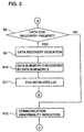
- Response state display 7 receives an instruction from main control circuit 11 and displays information related to the response state of IC card 100. More specifically, the display indicates the following contents according to state determination flag FLG.
- state determination flag FLG if the state of writing data into data holding memory 2 is normal, an indication that a normal response has been completed (normal communication completion indication) is given.
- data recovery indication when the state of writing data into data holding memory 2 is abnormal, but the data has been recovered using data in data protecting memory 3, an indication that the data has been recovered (data recovery indication) is given.
- an indication that the response has been abnormal (communication abnormality indication) is given.
- Power supply circuit 8 supplies power to response state display 7 for a prescribed time period.
- Response state display 7 receives the power supplied from power supply circuit 8 and continuously displays the response state for a prescribed time period.
- Power supply circuit 8 may be for example a circuit formed of a large capacity capacitor receiving current from rectifying circuit 16 shown in Fig. 6, or a circuit including a storage cell or a solar cell.
- IC card 100 The operation of IC card 100 according to the first embodiment will be now described.
- Figs. 2 and 3 are flow charts each for use in illustration of operations related to data holding and recovery operations by IC card 100 according to the first embodiment.
- state determination flag FLG takes 0 or 1, and the value is initialized to 0 if the state of writing data is normal.
- step S1 the IC card is activated.
- state determination flag FLG takes 0, in other words when the state of writing data in data holding memory 2 is normal will be described.
- IC card 100 performs a data communication using data in data holding memory 2.
- step S3 data DA is input to register 4. Data in region B1 in data holding memory 2 is then read out and the read out data is saved (written) in data protecting memory 3.
- step S4 state determination flag FLG is set to 1 (to the state in which data in region B1 in data holding memory 2 has been saved in data protecting memory 3).
- step S5 data DA written in register 4 is written in region B1 in data holding memory 2.
- state determination flag FLG takes 1, in other words, when the state of writing data in data holding memory 2 is abnormal will be now described.
- step S8 It is checked in step S8 if data necessary for recovering data in data holding memory 2 is present in data protecting memory 3. If no such data is present (such as in the first communication in which no data is present in data protecting memory 3), a communication abnormality occurs, and therefore response state display 7 gives a communication abnormality indication in step 12.
- step S10 data which has been saved in data protecting memory 3 is read out, and the data is written in region B1 in data holding memory 2. As a result, the data causing a communication abnormality is destroyed, and normal data is written (recovered) in data holding memory 2.
- Figs. 4A to 4C are views each showing an overview of IC card 100 according to the first embodiment.
- response state display 7 maybe formed using an LED (L1, L2, and L3 in Fig. 4A).
- L1, L2, and L3 in Fig. 4A may correspond to the normal communication indication, data recovery indication, and communication abnormality indication, respectively.
- the use of LEDs of two colors makes it easier for the user to visually recognize the normal communication indication and the communication abnormality indication.
- the content of display is not limited to the above, and other communication contents (L4, L5, L6, and L7 in Fig. 4B) may be indicated.
- response state display 7 may be formed by an LCD or by both an LCD (L8 in Fig. 4C) and an LED (L1, L2 in Fig. 4C).
- IC card 100 has a display function, may determine the state of writing data in data holding memory 2, and use the result of determination to externally display the response state of IC card 100 in a data communication.
- An IC card externally displays the response state of the IC card in a data communication using a main memory or a sub memory for holding data.
- Fig. 5 is a block diagram of the configuration of a main part of an IC card 200 according to the second embodiment, and the remaining part is the same as that of the conventional IC card 300 shown in Fig. 6 (except memory 10) and therefore is not shown or described.
- the card to which the invention is applied may be a contacting type or non-contacting type IC card.
- IC card 200 shown in Fig. 5 is different from the conventional IC card 300 in the following points.
- IC card 200 includes a non-volatile main memory for holding data 20 (hereinafter simply as main memory 20) and a non-volatile sub memory for holding data 21 (hereinafter simply as sub memory 21) in place of memory 10, detection circuits 22 and 23 for detecting errors in main memory 20 and sub memory 21, respectively, a response state display 30 for displaying a response state, and a power supply circuit 8 for supplying power to response state display 30 for a prescribed time period.
- IC card 200 Referring to Fig. 5, the configuration of IC card 200 according to the second embodiment will be described.
- Main memory 20 and sub memory 21 are connected to a main control circuit 11 through selectors 28 and 29, respectively.
- Sub memory 21 is used as a backup memory for main memory 20, and data corresponding on a one-to-one basis to data in main memory 20 is written in this sub memory. Note that the data written in sub memory 21 may be the inverse of data written in main memory 20, or data complementary to the data written in main memory 20.
- Main memory 20 and sub memory 21 may be formed by an EEPROM, a flash memory, a ferroelectric memory or the like.
- Error detection circuits 22 and 23 detect errors in data written in main memory 20 and sub memory 21, respectively. Error detection circuits 22 and 23 control selectors 28 and 29 based on the result of detection. As a result, a memory (main memory 20 or sub memory 21) which allows main control circuit 11 to read out data is selected.
- Error detection circuits 22 and 23 may be a parity check circuit, a CRC check circuit or the like. Errors may be detected on a one-bit-basis or a multi-byte-basis.
- Error correction circuits 26 and 27 correct errors detected by error detection circuits 22 and 23, respectively.
- Response state display 30 receives an instruction from main control circuit 11 and gives an indication related to the response state of IC card 200. More specifically, the indication is switched depending upon the error detection about main memory 20 and sub memory 21.
- Response state display 30 may be formed by an LCD or LED as described in conncetion with the first embodiment of the invention.
- Power supply circuit 8 supplies power to response state display 30 for a prescribed time period as described in connection with the first embodiment.
- IC card 200 The operation of IC card 200 according to the second embodiment will be now described.
- main control circuit 11 When main control circuit 11 receives data from an interrogator, main control circuit 11 has data DA stored in main memory 20 and sub memory 21 through selectors 28 and 29, respectively.
- Error detection circuit 22 detects the presence/absence of an error in the data stored in main memory 20. If an error is not detected in the data in main memory 20, error detection circuit 22 controls selector 28 such that the data is to be read out to main control circuit 11 from main memory 20, and controls selector 29 such that data is not to be read out from sub memory 21. Meanwhile, if an error is detected in the data in main memory 20, control circuit 11 controls selector 28 such that the data is not to be read out from main memory 20 and controls selector 29 such that data is to be read out from sub memory 21.
- Error detection circuit 23 detects the presence/absence of an error in the data stored in sub memory 21. If an error is detected in sub memory 21 as well as in main memory 20, data is not provided from main memory 20 and sub memory 21 to main control circuit 11. In this case, main control circuit 11 requests the interrogator to re-transmit the data or clearly indicates the presence of the error. If an error is detected, error correction circuits 26 and 27 read out data from main memory 20 or sub memory 21 and then correct the data.
- Response state display 30 makes a normal communication completion indication when data is read out from main memory 20 or sub memory 21 and gives a communication abnormality indication when no data is read out from any of memories 20 and 21.
- Response state display 30 may give a normal communication completion indication when data is read out from main memory 20, a backup indication when data is read out from sub memory 21, and a communication abnormality indication when no data is read out from any of memories 20 and 21.
- response state display 30 needs only be adapted to give a normal communication indication and a communication abnormality indication.
- IC card 200 having a display function may detect errors in data in main memory 20 and sub memory 21 and may externally display the response state of IC card 200 in a data communication based on the result of detection.
- an IC card according to the present invention has a display function and may externally display a response state in a data communication using the result of determination of the state of writing data.
- the response state may be continuously displayed for a prescribed time period.
- the reliability of the IC card may be improved.
Landscapes
- Engineering & Computer Science (AREA)
- Computer Hardware Design (AREA)
- Microelectronics & Electronic Packaging (AREA)
- Physics & Mathematics (AREA)
- General Physics & Mathematics (AREA)
- Theoretical Computer Science (AREA)
- Computer Security & Cryptography (AREA)
- General Engineering & Computer Science (AREA)
- Credit Cards Or The Like (AREA)
- Techniques For Improving Reliability Of Storages (AREA)
Applications Claiming Priority (3)
| Application Number | Priority Date | Filing Date | Title |
|---|---|---|---|
| JP3798097 | 1997-02-21 | ||
| JP3798097A JP3667920B2 (ja) | 1997-02-21 | 1997-02-21 | Icカード |
| PCT/JP1998/000059 WO1998037510A1 (en) | 1997-02-21 | 1998-01-09 | Ic card |
Publications (3)
| Publication Number | Publication Date |
|---|---|
| EP0991012A1 true EP0991012A1 (de) | 2000-04-05 |
| EP0991012A4 EP0991012A4 (de) | 2000-05-03 |
| EP0991012B1 EP0991012B1 (de) | 2001-12-05 |
Family
ID=12512726
Family Applications (1)
| Application Number | Title | Priority Date | Filing Date |
|---|---|---|---|
| EP98900201A Expired - Lifetime EP0991012B1 (de) | 1997-02-21 | 1998-01-09 | Chip-karte |
Country Status (9)
| Country | Link |
|---|---|
| US (1) | US6454172B1 (de) |
| EP (1) | EP0991012B1 (de) |
| JP (1) | JP3667920B2 (de) |
| KR (1) | KR100378224B1 (de) |
| CN (1) | CN1248337A (de) |
| AU (1) | AU5342698A (de) |
| CA (1) | CA2278346A1 (de) |
| DE (1) | DE69802805T2 (de) |
| WO (1) | WO1998037510A1 (de) |
Families Citing this family (18)
| Publication number | Priority date | Publication date | Assignee | Title |
|---|---|---|---|---|
| JP3567787B2 (ja) * | 1999-03-23 | 2004-09-22 | ミノルタ株式会社 | データ記憶媒体 |
| JP2002236891A (ja) * | 2001-02-08 | 2002-08-23 | Mitsubishi Heavy Ind Ltd | データ表示機能付き無線タグ |
| US7228469B2 (en) * | 2003-01-02 | 2007-06-05 | Fujitsu Limited | Portable information device, method for recovering data in portable information device, and computer product |
| US9022294B2 (en) * | 2003-04-14 | 2015-05-05 | G. Holdings Ltd. | Portable electronic device and method for alternate data conveyance operations responsive to an invariable activation command |
| WO2004090805A1 (en) * | 2003-04-14 | 2004-10-21 | G. Holdings Ltd. | Portable electronic device capable of alternate data conveyance operations responsive to an invariable activation command |
| ATE505032T1 (de) † | 2003-09-03 | 2011-04-15 | Visible Tech Knowledgy Inc | Elektronisch aktualisierbares label und display |
| GB2418036B (en) * | 2004-09-08 | 2007-10-31 | Advanced Risc Mach Ltd | Communication transaction control between independent domains of an integrated circuit |
| US8011592B2 (en) * | 2007-01-19 | 2011-09-06 | Sipix Imaging, Inc. | Temperature management in an integrated circuit card with electrophoretic display |
| JP5149746B2 (ja) * | 2008-09-10 | 2013-02-20 | パナソニック株式会社 | 薄型識別デバイス |
| EP2330539A4 (de) * | 2008-09-10 | 2014-09-24 | Panasonic Corp | Funkidentifikationskarte |
| JP5149747B2 (ja) * | 2008-09-11 | 2013-02-20 | パナソニック株式会社 | 非接触識別デバイスおよびそれを用いた非接触識別システム |
| JP2010067006A (ja) * | 2008-09-10 | 2010-03-25 | Panasonic Electric Works Co Ltd | 表示デバイス |
| JP4992924B2 (ja) * | 2009-03-12 | 2012-08-08 | オムロン株式会社 | Icカードおよびデータ送受信システム |
| TW201039242A (en) * | 2009-04-21 | 2010-11-01 | Princeton Technology Corp | IC card with display function |
| FR2949165B1 (fr) * | 2009-08-11 | 2011-10-07 | Oberthur Technologies | Carte a microcircuit comprenant une diode electroluminescente |
| TWI423142B (zh) * | 2009-09-09 | 2014-01-11 | Electronic display type smart card | |
| US20120226934A1 (en) * | 2011-03-01 | 2012-09-06 | Rao G R Mohan | Mission critical nand flash |
| DE102012102941A1 (de) * | 2012-04-04 | 2013-10-10 | Sportident Gmbh | Passiver RFID-Transponder mit Signalisierungseinrichtung sowie Verfahren zum Betreiben eines derartigen RFID-Transponders |
Family Cites Families (34)
| Publication number | Priority date | Publication date | Assignee | Title |
|---|---|---|---|---|
| SE411600B (sv) * | 1978-05-25 | 1980-01-14 | Trehn Karl Bengt | Speciellt for motorfordon avsett parkeringssystem |
| EP0247623A3 (en) | 1984-03-19 | 1989-09-20 | Omron Tateisi Electronics Co. | Ic card transaction system |
| DE3585464D1 (de) * | 1984-06-19 | 1992-04-09 | Casio Computer Co Ltd | Intelligente karte. |
| IL72802A (en) * | 1984-08-29 | 1990-01-18 | N T E Parkulator | Time metering device particularly useful as a parking card |
| US4614861A (en) * | 1984-11-15 | 1986-09-30 | Intellicard International, Inc. | Unitary, self-contained card verification and validation system and method |
| US4766293A (en) * | 1986-06-26 | 1988-08-23 | Visa International Service Association | Portable financial transaction card capable of authorizing a transaction in foreign currencies |
| JP2514954B2 (ja) * | 1987-03-13 | 1996-07-10 | 三菱電機株式会社 | Icカ−ド |
| JPS63226752A (ja) * | 1987-03-16 | 1988-09-21 | Omron Tateisi Electronics Co | Idシステムのデ−タ書込み方式 |
| US4868376A (en) * | 1987-05-15 | 1989-09-19 | Smartcard International Inc. | Intelligent portable interactive personal data system |
| JPH01189745A (ja) | 1988-01-25 | 1989-07-28 | Nec Corp | メモリ書込み方式 |
| JP2833136B2 (ja) | 1990-04-03 | 1998-12-09 | オムロン株式会社 | 非接触式記憶媒体処理システム |
| FR2666425A1 (fr) * | 1990-08-31 | 1992-03-06 | Gemplus Card Int | Procede et dispositif de mise a jour d'informations dans une memoire et leur utilisation dans les cartes a memoire. |
| JPH04113489A (ja) | 1990-09-04 | 1992-04-14 | Mitsubishi Electric Corp | 非接触icカード |
| US5659890A (en) * | 1991-07-25 | 1997-08-19 | Casio Computer Co., Ltd. | Portable radio apparatus equipped with function to display received message information |
| US5585787A (en) * | 1991-12-09 | 1996-12-17 | Wallerstein; Robert S. | Programmable credit card |
| GB9307623D0 (en) * | 1993-04-13 | 1993-06-02 | Jonhig Ltd | Data writing to eeprom |
| KR960005370Y1 (ko) * | 1993-12-09 | 1996-06-28 | 포항종합제철 주식회사 | 와이어식 벨트 클리너(Wire Belt Cleaner) |
| US5623552A (en) * | 1994-01-21 | 1997-04-22 | Cardguard International, Inc. | Self-authenticating identification card with fingerprint identification |
| US5479172A (en) | 1994-02-10 | 1995-12-26 | Racom Systems, Inc. | Power supply and power enable circuit for an RF/ID transponder |
| US5590038A (en) * | 1994-06-20 | 1996-12-31 | Pitroda; Satyan G. | Universal electronic transaction card including receipt storage and system and methods of conducting electronic transactions |
| JPH0830841A (ja) | 1994-07-11 | 1996-02-02 | Nec Corp | 音声案内可能表示入力機能付icカード |
| JP3406444B2 (ja) * | 1995-01-10 | 2003-05-12 | 富士通株式会社 | データ転送システムのバス制御装置 |
| JPH09114945A (ja) | 1995-10-20 | 1997-05-02 | Matsushita Electric Ind Co Ltd | 非接触icカード |
| EP0784301B1 (de) * | 1996-01-08 | 2002-10-16 | Jürgen Dethloff | Verfahren und System zum Bezahlen von Leistungen sowie tragbarer Datenträger für ein derartiges System |
| JPH09212598A (ja) * | 1996-01-31 | 1997-08-15 | Toshiba Corp | Icカード用携帯端末装置 |
| JPH09282862A (ja) * | 1996-04-11 | 1997-10-31 | Mitsubishi Electric Corp | メモリカード |
| JPH1011555A (ja) | 1996-06-25 | 1998-01-16 | Hitachi Ltd | 情報icカード |
| US5754762A (en) * | 1997-01-13 | 1998-05-19 | Kuo; Chih-Cheng | Secure multiple application IC card using interrupt instruction issued by operating system or application program to control operation flag that determines the operational mode of bi-modal CPU |
| JPH10260912A (ja) * | 1997-03-17 | 1998-09-29 | Mitsubishi Electric Corp | メモリカード |
| JP3822707B2 (ja) * | 1997-05-08 | 2006-09-20 | 株式会社ルネサステクノロジ | Icカード |
| JP3728366B2 (ja) * | 1997-05-13 | 2005-12-21 | 株式会社ルネサステクノロジ | Icカード |
| JPH10340575A (ja) * | 1997-06-04 | 1998-12-22 | Sony Corp | 外部記憶装置及びその制御装置、データ送受信装置 |
| US6019284A (en) * | 1998-01-27 | 2000-02-01 | Viztec Inc. | Flexible chip card with display |
| JP3288289B2 (ja) | 1998-03-16 | 2002-06-04 | 日本たばこ産業株式会社 | 異物排除装置 |
-
1997
- 1997-02-21 JP JP3798097A patent/JP3667920B2/ja not_active Expired - Fee Related
-
1998
- 1998-01-09 CA CA002278346A patent/CA2278346A1/en not_active Abandoned
- 1998-01-09 KR KR10-1999-7006193A patent/KR100378224B1/ko not_active Expired - Fee Related
- 1998-01-09 CN CN98802612A patent/CN1248337A/zh active Pending
- 1998-01-09 EP EP98900201A patent/EP0991012B1/de not_active Expired - Lifetime
- 1998-01-09 WO PCT/JP1998/000059 patent/WO1998037510A1/ja not_active Ceased
- 1998-01-09 DE DE69802805T patent/DE69802805T2/de not_active Expired - Fee Related
- 1998-01-09 US US09/341,116 patent/US6454172B1/en not_active Expired - Fee Related
- 1998-01-09 AU AU53426/98A patent/AU5342698A/en not_active Abandoned
Also Published As
| Publication number | Publication date |
|---|---|
| DE69802805D1 (de) | 2002-01-17 |
| CA2278346A1 (en) | 1998-08-27 |
| KR100378224B1 (ko) | 2003-03-29 |
| EP0991012A4 (de) | 2000-05-03 |
| AU5342698A (en) | 1998-09-09 |
| EP0991012B1 (de) | 2001-12-05 |
| JP3667920B2 (ja) | 2005-07-06 |
| WO1998037510A1 (en) | 1998-08-27 |
| US6454172B1 (en) | 2002-09-24 |
| DE69802805T2 (de) | 2002-06-13 |
| KR20000069978A (ko) | 2000-11-25 |
| CN1248337A (zh) | 2000-03-22 |
| JPH10240873A (ja) | 1998-09-11 |
Similar Documents
| Publication | Publication Date | Title |
|---|---|---|
| US6454172B1 (en) | IC card having a display for displaying a response state | |
| US4877945A (en) | IC card having a function to exclude erroneous recording | |
| US4779091A (en) | Radio pager receiver capable of informing whether or not memory backup is correct | |
| US20010045468A1 (en) | Ic card | |
| CN111459721B (zh) | 故障处理方法、装置和计算机 | |
| JP2000035923A (ja) | 異常検出方法および異常検出装置 | |
| JPH10187550A (ja) | Icカード | |
| JPH05297128A (ja) | 個体識別装置 | |
| JPH05250531A (ja) | Icカード | |
| JPH1153487A (ja) | Icカードにおける書き込みデータの有効性判定方法 | |
| JP3230743B2 (ja) | メモリカードのデータ不一致検出方式及びその方法 | |
| JPS63268085A (ja) | 携帯可能記憶媒体読取書込装置 | |
| JPH0376515B2 (de) | ||
| JPH10105659A (ja) | 非接触icカード | |
| JPH06290112A (ja) | Eepromによるビットデータ記憶装置 | |
| JPS59173899A (ja) | 遠方監視装置における表示方式 | |
| JPH01248289A (ja) | Icカードの異常検出装置 | |
| JPH06202961A (ja) | メモリテスト機能内蔵のマイクロコンピュータ | |
| JPH04152488A (ja) | Icカード | |
| JPH09212368A (ja) | リモートローディング伝送装置 | |
| JPH0595510A (ja) | 更新画面制御装置 | |
| JPH047765A (ja) | E↑2promのデータ読込装置 | |
| JPH02171991A (ja) | Icカードの制御方法 | |
| JPH0359740A (ja) | メモリ障害検出方式 | |
| JPH10187551A (ja) | Icカード |
Legal Events
| Date | Code | Title | Description |
|---|---|---|---|
| PUAI | Public reference made under article 153(3) epc to a published international application that has entered the european phase |
Free format text: ORIGINAL CODE: 0009012 |
|
| 17P | Request for examination filed |
Effective date: 19990723 |
|
| AK | Designated contracting states |
Kind code of ref document: A1 Designated state(s): DE FR GB |
|
| A4 | Supplementary search report drawn up and despatched |
Effective date: 20000320 |
|
| AK | Designated contracting states |
Kind code of ref document: A4 Designated state(s): DE FR GB |
|
| 17Q | First examination report despatched |
Effective date: 20000703 |
|
| GRAG | Despatch of communication of intention to grant |
Free format text: ORIGINAL CODE: EPIDOS AGRA |
|
| GRAG | Despatch of communication of intention to grant |
Free format text: ORIGINAL CODE: EPIDOS AGRA |
|
| GRAH | Despatch of communication of intention to grant a patent |
Free format text: ORIGINAL CODE: EPIDOS IGRA |
|
| GRAH | Despatch of communication of intention to grant a patent |
Free format text: ORIGINAL CODE: EPIDOS IGRA |
|
| GRAA | (expected) grant |
Free format text: ORIGINAL CODE: 0009210 |
|
| AK | Designated contracting states |
Kind code of ref document: B1 Designated state(s): DE FR GB |
|
| REG | Reference to a national code |
Ref country code: GB Ref legal event code: IF02 |
|
| PGFP | Annual fee paid to national office [announced via postgrant information from national office to epo] |
Ref country code: GB Payment date: 20020116 Year of fee payment: 5 |
|
| REF | Corresponds to: |
Ref document number: 69802805 Country of ref document: DE Date of ref document: 20020117 |
|
| ET | Fr: translation filed | ||
| PLBE | No opposition filed within time limit |
Free format text: ORIGINAL CODE: 0009261 |
|
| STAA | Information on the status of an ep patent application or granted ep patent |
Free format text: STATUS: NO OPPOSITION FILED WITHIN TIME LIMIT |
|
| 26N | No opposition filed | ||
| PG25 | Lapsed in a contracting state [announced via postgrant information from national office to epo] |
Ref country code: GB Free format text: LAPSE BECAUSE OF NON-PAYMENT OF DUE FEES Effective date: 20030109 |
|
| GBPC | Gb: european patent ceased through non-payment of renewal fee |
Effective date: 20030109 |
|
| PGFP | Annual fee paid to national office [announced via postgrant information from national office to epo] |
Ref country code: DE Payment date: 20090102 Year of fee payment: 12 |
|
| PGFP | Annual fee paid to national office [announced via postgrant information from national office to epo] |
Ref country code: FR Payment date: 20090113 Year of fee payment: 12 |
|
| REG | Reference to a national code |
Ref country code: FR Ref legal event code: ST Effective date: 20100930 |
|
| PG25 | Lapsed in a contracting state [announced via postgrant information from national office to epo] |
Ref country code: FR Free format text: LAPSE BECAUSE OF NON-PAYMENT OF DUE FEES Effective date: 20100201 |
|
| PG25 | Lapsed in a contracting state [announced via postgrant information from national office to epo] |
Ref country code: DE Free format text: LAPSE BECAUSE OF NON-PAYMENT OF DUE FEES Effective date: 20100803 |