EP0996323A2 - Bauteil für die Oberflächenmontage - Google Patents
Bauteil für die Oberflächenmontage Download PDFInfo
- Publication number
- EP0996323A2 EP0996323A2 EP99119684A EP99119684A EP0996323A2 EP 0996323 A2 EP0996323 A2 EP 0996323A2 EP 99119684 A EP99119684 A EP 99119684A EP 99119684 A EP99119684 A EP 99119684A EP 0996323 A2 EP0996323 A2 EP 0996323A2
- Authority
- EP
- European Patent Office
- Prior art keywords
- electronic parts
- printed board
- mounting part
- surface mounting
- board
- Prior art date
- Legal status (The legal status is an assumption and is not a legal conclusion. Google has not performed a legal analysis and makes no representation as to the accuracy of the status listed.)
- Granted
Links
Images


Classifications
-
- H—ELECTRICITY
- H05—ELECTRIC TECHNIQUES NOT OTHERWISE PROVIDED FOR
- H05K—PRINTED CIRCUITS; CASINGS OR CONSTRUCTIONAL DETAILS OF ELECTRIC APPARATUS; MANUFACTURE OF ASSEMBLAGES OF ELECTRICAL COMPONENTS
- H05K1/00—Printed circuits
- H05K1/02—Details
- H05K1/14—Structural association of two or more printed circuits
- H05K1/145—Arrangements wherein electric components are disposed between and simultaneously connected to two planar printed circuit boards, e.g. Cordwood modules
-
- H—ELECTRICITY
- H05—ELECTRIC TECHNIQUES NOT OTHERWISE PROVIDED FOR
- H05K—PRINTED CIRCUITS; CASINGS OR CONSTRUCTIONAL DETAILS OF ELECTRIC APPARATUS; MANUFACTURE OF ASSEMBLAGES OF ELECTRICAL COMPONENTS
- H05K3/00—Apparatus or processes for manufacturing printed circuits
- H05K3/30—Assembling printed circuits with electric components, e.g. with resistors
-
- H—ELECTRICITY
- H05—ELECTRIC TECHNIQUES NOT OTHERWISE PROVIDED FOR
- H05K—PRINTED CIRCUITS; CASINGS OR CONSTRUCTIONAL DETAILS OF ELECTRIC APPARATUS; MANUFACTURE OF ASSEMBLAGES OF ELECTRICAL COMPONENTS
- H05K1/00—Printed circuits
- H05K1/02—Details
- H05K1/14—Structural association of two or more printed circuits
- H05K1/141—One or more single auxiliary printed circuits mounted on a main printed circuit, e.g. modules, adapters
-
- H—ELECTRICITY
- H05—ELECTRIC TECHNIQUES NOT OTHERWISE PROVIDED FOR
- H05K—PRINTED CIRCUITS; CASINGS OR CONSTRUCTIONAL DETAILS OF ELECTRIC APPARATUS; MANUFACTURE OF ASSEMBLAGES OF ELECTRICAL COMPONENTS
- H05K2201/00—Indexing scheme relating to printed circuits covered by H05K1/00
- H05K2201/09—Shape and layout
- H05K2201/09145—Edge details
- H05K2201/09181—Notches in edge pads
-
- H—ELECTRICITY
- H05—ELECTRIC TECHNIQUES NOT OTHERWISE PROVIDED FOR
- H05K—PRINTED CIRCUITS; CASINGS OR CONSTRUCTIONAL DETAILS OF ELECTRIC APPARATUS; MANUFACTURE OF ASSEMBLAGES OF ELECTRICAL COMPONENTS
- H05K2201/00—Indexing scheme relating to printed circuits covered by H05K1/00
- H05K2201/10—Details of components or other objects attached to or integrated in a printed circuit board
- H05K2201/10227—Other objects, e.g. metallic pieces
- H05K2201/10371—Shields or metal cases
-
- H—ELECTRICITY
- H05—ELECTRIC TECHNIQUES NOT OTHERWISE PROVIDED FOR
- H05K—PRINTED CIRCUITS; CASINGS OR CONSTRUCTIONAL DETAILS OF ELECTRIC APPARATUS; MANUFACTURE OF ASSEMBLAGES OF ELECTRICAL COMPONENTS
- H05K2201/00—Indexing scheme relating to printed circuits covered by H05K1/00
- H05K2201/10—Details of components or other objects attached to or integrated in a printed circuit board
- H05K2201/10613—Details of electrical connections of non-printed components, e.g. special leads
- H05K2201/10621—Components characterised by their electrical contacts
- H05K2201/10636—Leadless chip, e.g. chip capacitor or resistor
-
- H—ELECTRICITY
- H05—ELECTRIC TECHNIQUES NOT OTHERWISE PROVIDED FOR
- H05K—PRINTED CIRCUITS; CASINGS OR CONSTRUCTIONAL DETAILS OF ELECTRIC APPARATUS; MANUFACTURE OF ASSEMBLAGES OF ELECTRICAL COMPONENTS
- H05K3/00—Apparatus or processes for manufacturing printed circuits
- H05K3/30—Assembling printed circuits with electric components, e.g. with resistors
- H05K3/32—Assembling printed circuits with electric components, e.g. with resistors electrically connecting electric components or wires to printed circuits
- H05K3/34—Assembling printed circuits with electric components, e.g. with resistors electrically connecting electric components or wires to printed circuits by soldering
- H05K3/341—Surface mounted components
- H05K3/3431—Leadless components
- H05K3/3442—Leadless components having edge contacts, e.g. leadless chip capacitors, chip carriers
-
- H—ELECTRICITY
- H05—ELECTRIC TECHNIQUES NOT OTHERWISE PROVIDED FOR
- H05K—PRINTED CIRCUITS; CASINGS OR CONSTRUCTIONAL DETAILS OF ELECTRIC APPARATUS; MANUFACTURE OF ASSEMBLAGES OF ELECTRICAL COMPONENTS
- H05K3/00—Apparatus or processes for manufacturing printed circuits
- H05K3/36—Assembling printed circuits with other printed circuits
- H05K3/368—Assembling printed circuits with other printed circuits parallel to each other
-
- Y—GENERAL TAGGING OF NEW TECHNOLOGICAL DEVELOPMENTS; GENERAL TAGGING OF CROSS-SECTIONAL TECHNOLOGIES SPANNING OVER SEVERAL SECTIONS OF THE IPC; TECHNICAL SUBJECTS COVERED BY FORMER USPC CROSS-REFERENCE ART COLLECTIONS [XRACs] AND DIGESTS
- Y02—TECHNOLOGIES OR APPLICATIONS FOR MITIGATION OR ADAPTATION AGAINST CLIMATE CHANGE
- Y02P—CLIMATE CHANGE MITIGATION TECHNOLOGIES IN THE PRODUCTION OR PROCESSING OF GOODS
- Y02P70/00—Climate change mitigation technologies in the production process for final industrial or consumer products
- Y02P70/50—Manufacturing or production processes characterised by the final manufactured product
Definitions
- the present invention relates to a surface mounting part (module) having a configuration with electronic parts mounted on a printed circuit board for providing a module, and mounted on a mother board, such as a voltage controlled oscillator, and in particular, it relates to a structure for downsizing a module.
- conventional voltage controlled oscillators used in mobile communication devices comprise a printed board 20 having a multi-layer structure of a conductor and an insulator, elements constituting an oscillator, such as a resonator and a capacitor, formed inside, and a plurality of other electronic parts 21, such as a capacitor, a semiconductor element, mounted on the surface of the printed board 20.
- a shield case 22 is provided so as to cover the electronic part 21 for preventing the noise radiation from the electronic part 22 to the outside and entrance of the noise from the outside.
- the shield case 22 is fixed by fitting projection pieces 22a, elongating from the lower opening side rim of the shield case 22, to semi-circular arc-like terminals 23, 24 provided on both side surfaces of the printed board 20, and soldering.
- terminal electrodes 26 to 31 to serve as a power source terminal, an input terminal, an output terminal and a ground terminal, are formed on the periphery of the printed board 20.
- the voltage controlled oscillator is fixed by electrically connecting the terminal electrodes 26 to 31 to a pad 34 on a mother board 33 by reflow as shown in FIG. 4C.
- the official gazette of JP-A-6-111869 discloses an embodiment comprising a module with electronic parts 39 mounted on the front and rear sides of a printed board 37.
- the module circuit board (printed board) 37 disclosed in the official gazette is fixed by soldering to a mother board 42 via block-like terminal members 41 comprising a conductor film formed on the periphery of an insulator.
- the mother board 33 needs to be downsized.
- the printed board 20, 37 needs to be smaller for downsizing the module.
- the configuration comprising the electronic parts 21 mounted on one side of the printed board 20 involves a problem in that since the number of the electronic parts 21 to be mounted is set to some extent, the size of the printed board 20 is limited and further downsizing of the module is disabled.
- the electronic parts 39 are mounted on the front and rear sides of the printed board 37 as disclosed in the official gazette, the electronic parts 39 are allotted on the front and rear sides, and thus a problem of the mounting space of the electronic parts can be alleviated.
- the configuration disclosed in the official gazette involves a problem in that a space for attaching the block-like terminal members 41 is required on the rear side of the peripheral part of the printed board 37 in place of lead terminals so as to disturb downsizing.
- lead terminals conventionally used are used in place of the block-like terminal members 41, also a problem is involved in that a space for connecting the lead terminals is required so as to disturb downsizing.
- an object of the invention is to provide a surface mounting part, capable of corresponding to high density mounting of a mother board and capable of achieving a small size.
- a first aspect of a surface mounting part comprises electronic parts on both sides of a printed board, wherein terminal electrodes of the electronic parts mounted on the rear side serve as the terminals to be connected with a mother board.
- terminal electrodes of the electronic parts mounted on the rear side serve also as the terminals for connecting with the outside of the surface mounting part
- a space for attaching a connecting member for connecting the surface mounting part with the mother board is not required so as to enable downsizing of the printed board, that is, downsizing of the surface mounting part.
- the surface mounting part is a voltage controlled oscillator.
- the voltage controlled oscillator can be downsized, and thus a mobile communication device comprising the same can be downsized as well.
- a solder for connecting the printed board and the electronic parts mounted on the rear side is of a high melting temperature type, that is, a high melting point, which is different from the melting temperature of an eutectic solder for connecting with the mother board so as to prevent displacement of the electronic parts used as the terminal electrodes with respect to the printed board.
- terminal electrodes not connected with the mother board are covered with an insulating material.
- terminal electrodes not connected with the mother board are covered with an insulating material, insulation can be ensured without the risk of contacting with the conductor pattern on the mother board side.
- a space between the electronic parts mounted on the rear side of the printed board is filled with an insulating material.
- the surface mounting part is soldered on the mother board by reflow
- the solder for fixing the electronic parts on the printed board in particular, on the rear side
- a solder having a higher melting point with respect to the solder for fixing the surface mounting part on the mother board is used for fixing the electronic parts on the printed board, displacement of the electronic parts can be prevented, and positioning and fixing can be facilitated.
- the risk of melting is large. If the melting takes place, the electronic parts mounted on the printed board may be displaced. That is, since the pads of the mother board and the printed board are soldered with each other, displacement takes place toward a larger tensile force side.
- the configuration of the fourth aspect wherein a space between the electronic parts mounted on the rear side of the printed board is filled with an insulating material, displacement of the electronic parts can be prevented, and positioning and fixing can be facilitated.
- the electronic parts mounted on the rear side of the printed board have terminal electrodes on both ends, and the terminal electrodes on one end side are connected with the printed board, and the terminal electrodes on the other end are connected with the mother board.
- the terminal electrodes on the side not connected with the mother board can avoid the risk of contacting with the conductor pattern of the mother board.
- FIG. 1A is a perspective view of an embodiment of a surface mounting part according to the invention viewed from the front side
- FIG. 1B is a perspective view of the surface mounting part viewed from the rear side
- FIG. 1C is a perspective view of the surface mounting part in the state with a shield case attached.
- FIGS. 2A and 2B show the state of the surface mounting part mounted on the mother board, viewed from the X direction and the Y direction of FIG. 1A, respectively.
- numeral 1 denotes a printed board.
- a voltage controlled oscillator is presented as an example thereof.
- the printed board 1 has a multi-layer structure of a conductor and an insulator (including a dielectric substance, a magnetic substance and a non-magnetic substance) by a screen printing process or a sheet process so as to form a resonator, a capacitor, and a through hole for connection in the inside as well as to optionally form an inductor and a resistor in the inside, and a conductor pattern on the front and rear sides.
- any one selected from the group consisting of a capacitor, an inductor and a resistor is mounted as an electronic part 2 on the surface of the printed board 1.
- An electronic part 3 comprising a capacitor is mounted on the rear side of the printed board 1, and furthermore, optionally either of a resistor or a inductor, or both of them may be mounted on the rear side.
- Semi-circular arc-like terminals 4 are formed on both sides of the printed board 1 by cutting a through hole with a conductor film formed on the inner wall.
- a shield case 5 is fixed so as to cover the electronic parts 2 on the surface of the printed board 1 by fitting and soldering projection pieces 5a projecting downward, formed on the rim of the lower opening part of the shield case 5 with the semi-circular arc-like terminals 4.
- electronic parts (in this embodiment, capacitors) 3 are mounted on the rear side of the printed board 1.
- the electronic parts 3 are fixed by electrically connecting terminal electrodes 3a, 3b provided on both ends with pads 6, 7 of the printed board 1 by a solder 9. Then, the terminal electrodes 3a of the electronic parts 3 on one end are connected electrically with pads 11 formed on the mother board 10 so as to be fixed.
- Numeral 13 denotes an electronic part directly mounted on the mother board 10.
- Electronic parts relatively unsusceptible to suffer the influence of a noise such as a capacitor to be connected with an input terminal, an output terminal, and a power source terminal of a voltage controlled oscillator, and a capacitor having each one end connected with a ground as well as to be connected with an input or output pad, a power source supply pad or a ground pad on the mother board 10, are selected as these electronic parts 3.
- a noise such as a capacitor to be connected with an input terminal, an output terminal, and a power source terminal of a voltage controlled oscillator, and a capacitor having each one end connected with a ground as well as to be connected with an input or output pad, a power source supply pad or a ground pad on the mother board 10.
- the thickness of the plurality of the electronic parts 3 having the terminals 3a to be connected with the mother board 10 is set to have the lower surface thereof flush with each other.
- the terminal electrodes 3a of the electronic parts 3 mounted on the rear side of the printed board 1 also serving as the terminals to be connected with the outside, a space for attaching a connecting member for connecting the surface mounting part 3 with the mother board, such as a lead terminal is not required so that downsizing of the printed board, that is, downsizing of the surface mounting part can be enabled.
- the printed board 1 having a multi-layer structure accommodates a part of or all of a resonator, a capacitor, an inductor, a resistor, a through hole for connection in the inside, the number of parts to be mounted can be reduced so that downsizing can be further facilitated as a whole.
- the conventional example compared with the conventional example with the electronic parts mounted only on one side, that is, the conventional example needs to have a large number of the terminals for connecting with the outside 26 to 31 in the periphery of the board whereas they are not required in the case of the invention so that in addition to downsizing by allotting the electronic parts onto the front and rear sides, a space required can further be smaller, and thus compared with the conventional example shown in FIG. 4A, the area of the printed board 1 can be made smaller to about 47% according to the invention.
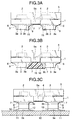
- FIG. 3A is a side view of a surface mounting part according to another embodiment of the invention.
- the terminal electrodes 3a on one end out of the plurality of the terminals 3a, 3b to be connected and fixed with the printed board 1 are used as the connection terminals with the mother board 10
- the terminal electrodes 3b not to be used as the connection terminals with the mother board 10 are covered with an insulating material 15, such as an insulating resin, at least on the mother board 10 side.
- the solder at portions 9, at which the terminals of the electronic parts and the printed board of the surface mounting part are connected in FIGS. 2A, 2B, 3A, 3B and 3C, has a higher melting point with respect to an eutectic solder for fixing the surface mounting part on the mother board.
- the solder has the higher melting point about 210°C to 250°C, while the eutectic solder has the melting point about 180°C.
- the terminal electrodes 3b not to be used as the connection terminals with the mother board 10 are covered with the insulating material 15, insulation can be ensured without the risk of contacting with the mother board side conductor pattern.
- FIG. 3B shows a modified embodiment of FIG. 3A.
- a space between the electronic parts 3 having the terminal electrodes 3a to be connected with the mother board 10 is covered with the insulating material 15, such as an insulating resin.
- the insulating material 15 such as an insulating resin.
- the electronic part 16 having a terminal not to be connected with the mother board 10 has a thickness set to be smaller than that of the electronic parts 3.
- FIG. 3C shows another embodiment of a surface mounting part of the invention.
- the electronic parts 3 mounted on the rear side of the printed board 1 and connected with the mother board 10 comprise the terminal electrodes 3a, 3b on both ends, with the terminal electrodes 3b connected with pads 7 of the printed board 1, and the terminal electrodes 3a on the other end connected with pads 11 of the mother board 10.
- the terminal electrodes 3b on the side not connected with the mother board 10 can avoid the risk of contacting with the conductor pattern of the mother board 10. Therefore, an insulating material needs not be provided for covering the terminal electrodes 3b on the printed board 1 side.
- the invention can be adopted not only to a voltage controlled oscillator, but also various kinds of modules with a relatively large number of parts, such as an active filter.
- the surface mounted part comprises electronic parts on both sides of a printed board, and terminal electrodes of the electronic parts mounted on the rear side serve as the terminals to be connected with a mother board, so that the electronic parts can be allotted on the front and rear sides of the printed board as well as a space for attaching a connecting member for connecting the surface mounting part with the mother board is not required, downsizing of the printed board, that is, downsizing of the surface mounting part can be enabled.
- the voltage controlled oscillator can be downsized, and thus a mobile communication device comprising the same can be downsized as well.
- the surface mounting part is soldered on the mother board by reflow
- the solder for fixing the electronic parts on the printed board in particular, on the rear side
- a solder having a higher melting point with respect to the solder for fixing the surface mounting part on the mother board is used for fixing the electronic parts on the printed board, displacement of the electronic parts can be prevented, and positioning and fixing can be facilitated.
- terminal electrodes not connected with the mother board provided in the electronic parts mounted on the rear side of the printed board having the terminals connected with the mother board, are covered with an insulating material, insulation can be ensured without the risk of contacting with the conductor pattern on the mother board side.
- the insulating material can serve as a fixing material so that displacement of the electronic parts caused by melting of the solder which fixes the electronic parts on the printed board at the time of mounting the surface mounting part on the mother board can be prevented, and positioning and fixing can be facilitated.
- the terminal electrodes on the side not connected with the mother board can avoid the risk of contacting with the conductor pattern of the mother board.
Landscapes
- Engineering & Computer Science (AREA)
- Microelectronics & Electronic Packaging (AREA)
- Manufacturing & Machinery (AREA)
- Combinations Of Printed Boards (AREA)
- Structures For Mounting Electric Components On Printed Circuit Boards (AREA)
- Oscillators With Electromechanical Resonators (AREA)
- Piezo-Electric Or Mechanical Vibrators, Or Delay Or Filter Circuits (AREA)
Applications Claiming Priority (2)
| Application Number | Priority Date | Filing Date | Title |
|---|---|---|---|
| JP28576698 | 1998-10-07 | ||
| JP10285766A JP2000114686A (ja) | 1998-10-07 | 1998-10-07 | 表面実装部品 |
Publications (3)
| Publication Number | Publication Date |
|---|---|
| EP0996323A2 true EP0996323A2 (de) | 2000-04-26 |
| EP0996323A3 EP0996323A3 (de) | 2000-05-03 |
| EP0996323B1 EP0996323B1 (de) | 2008-07-02 |
Family
ID=17695784
Family Applications (1)
| Application Number | Title | Priority Date | Filing Date |
|---|---|---|---|
| EP99119684A Expired - Lifetime EP0996323B1 (de) | 1998-10-07 | 1999-10-05 | Bauteil für die Oberflächenmontage |
Country Status (6)
| Country | Link |
|---|---|
| US (1) | US6373714B1 (de) |
| EP (1) | EP0996323B1 (de) |
| JP (1) | JP2000114686A (de) |
| KR (1) | KR100676546B1 (de) |
| DE (1) | DE69938997D1 (de) |
| MY (1) | MY121435A (de) |
Cited By (3)
| Publication number | Priority date | Publication date | Assignee | Title |
|---|---|---|---|---|
| DE10223998A1 (de) * | 2002-05-29 | 2003-12-11 | Vishay Electronic Gmbh | Elektrisches Modul |
| DE102006053461A1 (de) * | 2006-11-09 | 2008-05-15 | Fraunhofer-Gesellschaft zur Förderung der angewandten Forschung e.V. | Mikroelektronische Baugruppe und Verfahren zum Herstellen einer mikroelektronischen Baugruppe |
| WO2009083890A1 (en) * | 2007-12-27 | 2009-07-09 | Nxp B.V. | Apparatus and method for chip-scale package with capacitors as bumps |
Families Citing this family (26)
| Publication number | Priority date | Publication date | Assignee | Title |
|---|---|---|---|---|
| US6142361A (en) * | 1999-12-09 | 2000-11-07 | International Business Machines Corporation | Chip C4 assembly improvement using magnetic force and adhesive |
| JP2002094204A (ja) * | 2000-09-19 | 2002-03-29 | Matsushita Electric Ind Co Ltd | 高周波モジュールとその製造方法 |
| JP3768908B2 (ja) * | 2001-03-27 | 2006-04-19 | キヤノン株式会社 | 電子放出素子、電子源、画像形成装置 |
| TW497126B (en) * | 2001-05-03 | 2002-08-01 | Comchip Technology Co Ltd | Discrete circuit component and its manufacturing method |
| JP4810772B2 (ja) * | 2001-07-31 | 2011-11-09 | パナソニック株式会社 | 回路モジュール |
| US6609915B2 (en) * | 2001-11-30 | 2003-08-26 | Fci Americas Technology | Interconnect for electrically connecting a multichip module to a circuit substrate and processes for making and using same |
| US6900991B2 (en) * | 2001-12-03 | 2005-05-31 | Intel Corporation | Electronic assembly with sandwiched capacitors and methods of manufacture |
| JP2004119601A (ja) * | 2002-09-25 | 2004-04-15 | Fujitsu Ltd | 回路基板および電子機器 |
| TWI228286B (en) * | 2003-11-24 | 2005-02-21 | Ind Tech Res Inst | Bonding structure with buffer layer and method of forming the same |
| US8520402B1 (en) * | 2005-10-25 | 2013-08-27 | Xilinx, Inc. | Decoupling capacitor circuit assembly |
| DE102005060081B4 (de) * | 2005-12-15 | 2007-08-30 | Infineon Technologies Ag | Elektronisches Bauteil mit zumindest einer Leiterplatte und mit einer Mehrzahl gleichartiger Halbleiterbausteine und Verfahren |
| US8319114B2 (en) * | 2008-04-02 | 2012-11-27 | Densel Lambda K.K. | Surface mount power module dual footprint |
| US9955582B2 (en) * | 2008-04-23 | 2018-04-24 | Skyworks Solutions, Inc. | 3-D stacking of active devices over passive devices |
| JP4985852B2 (ja) * | 2008-11-04 | 2012-07-25 | 株式会社村田製作所 | 実装型電子回路モジュール |
| US20120171556A1 (en) * | 2010-12-29 | 2012-07-05 | Jongpil Kim | Secondary battery |
| US8767408B2 (en) * | 2012-02-08 | 2014-07-01 | Apple Inc. | Three dimensional passive multi-component structures |
| DE102013001006B4 (de) * | 2013-01-22 | 2015-01-22 | Baumüller Nürnberg GmbH | Leiterplattenanordnung |
| JP6272648B2 (ja) | 2013-01-30 | 2018-01-31 | 矢崎総業株式会社 | 熱干渉対策を考慮したヒートシンクレス電子ユニット |
| WO2018037969A1 (ja) * | 2016-08-24 | 2018-03-01 | 株式会社村田製作所 | 回路モジュール |
| KR102803439B1 (ko) * | 2016-11-01 | 2025-05-07 | 삼성전기주식회사 | 적층 전자 부품 |
| KR102067176B1 (ko) * | 2017-10-19 | 2020-01-15 | 삼성전기주식회사 | 적층형 전자 부품 및 그 실장 기판 |
| US10609844B1 (en) * | 2019-02-03 | 2020-03-31 | Hong Kong Applied Science and Technology Research Institute Company Limited | Power converter |
| JPWO2020174941A1 (ja) * | 2019-02-28 | 2021-12-23 | ソニーグループ株式会社 | 電子機器及び基板 |
| WO2022091479A1 (ja) * | 2020-10-30 | 2022-05-05 | 株式会社村田製作所 | 電源回路モジュール |
| US11641717B2 (en) | 2021-08-30 | 2023-05-02 | International Business Machines Corporation | Soldering of end chip components in series |
| TWI845267B (zh) * | 2023-04-20 | 2024-06-11 | 宜鼎國際股份有限公司 | 高電容量模組 |
Family Cites Families (14)
| Publication number | Priority date | Publication date | Assignee | Title |
|---|---|---|---|---|
| JPH01146391A (ja) * | 1987-12-02 | 1989-06-08 | Nec Corp | 混成集積回路装置 |
| JPH01191491A (ja) * | 1988-01-27 | 1989-08-01 | Matsushita Electric Ind Co Ltd | 多重回路板 |
| JPH0590728A (ja) * | 1991-09-27 | 1993-04-09 | Toshiba Lighting & Technol Corp | 混成集積回路基板 |
| JP2705408B2 (ja) * | 1991-11-20 | 1998-01-28 | 日本電気株式会社 | 混成集積回路装置 |
| JP3212717B2 (ja) | 1992-09-18 | 2001-09-25 | ティーディーケイ株式会社 | 積層混成集積回路部品 |
| JPH06111869A (ja) * | 1992-09-29 | 1994-04-22 | Fujitsu Ltd | 表面実装用端子 |
| JPH06164096A (ja) * | 1992-11-24 | 1994-06-10 | Tokyo Electric Co Ltd | 回路基板 |
| JPH06160183A (ja) | 1992-11-24 | 1994-06-07 | Tdk Corp | 赤外線検出器 |
| JPH06268365A (ja) * | 1993-03-16 | 1994-09-22 | Hitachi Ltd | 電子回路部品の実装方法 |
| JP2792473B2 (ja) * | 1995-07-06 | 1998-09-03 | 日本電気株式会社 | マルチチップモジュール |
| JP2938820B2 (ja) * | 1996-03-14 | 1999-08-25 | ティーディーケイ株式会社 | 高周波モジュール |
| US6125039A (en) * | 1996-07-31 | 2000-09-26 | Taiyo Yuden Co., Ltd. | Hybrid module |
| JP2845227B2 (ja) * | 1996-11-29 | 1999-01-13 | 日本電気株式会社 | マルチチップモジュールの実装構造 |
| US6142831A (en) * | 1999-02-01 | 2000-11-07 | Aux Corporation | Multifunction connector assembly |
-
1998
- 1998-10-07 JP JP10285766A patent/JP2000114686A/ja active Pending
-
1999
- 1999-10-04 KR KR1019990042542A patent/KR100676546B1/ko not_active Expired - Fee Related
- 1999-10-05 EP EP99119684A patent/EP0996323B1/de not_active Expired - Lifetime
- 1999-10-05 DE DE69938997T patent/DE69938997D1/de not_active Expired - Lifetime
- 1999-10-05 US US09/412,757 patent/US6373714B1/en not_active Expired - Fee Related
- 1999-10-06 MY MYPI99004310A patent/MY121435A/en unknown
Cited By (3)
| Publication number | Priority date | Publication date | Assignee | Title |
|---|---|---|---|---|
| DE10223998A1 (de) * | 2002-05-29 | 2003-12-11 | Vishay Electronic Gmbh | Elektrisches Modul |
| DE102006053461A1 (de) * | 2006-11-09 | 2008-05-15 | Fraunhofer-Gesellschaft zur Förderung der angewandten Forschung e.V. | Mikroelektronische Baugruppe und Verfahren zum Herstellen einer mikroelektronischen Baugruppe |
| WO2009083890A1 (en) * | 2007-12-27 | 2009-07-09 | Nxp B.V. | Apparatus and method for chip-scale package with capacitors as bumps |
Also Published As
| Publication number | Publication date |
|---|---|
| EP0996323A3 (de) | 2000-05-03 |
| DE69938997D1 (de) | 2008-08-14 |
| US6373714B1 (en) | 2002-04-16 |
| MY121435A (en) | 2006-01-28 |
| EP0996323B1 (de) | 2008-07-02 |
| JP2000114686A (ja) | 2000-04-21 |
| KR100676546B1 (ko) | 2007-01-30 |
| KR20000047509A (ko) | 2000-07-25 |
Similar Documents
| Publication | Publication Date | Title |
|---|---|---|
| US6373714B1 (en) | Surface mounting part | |
| US6373366B1 (en) | Common mode filter | |
| CN1756474B (zh) | 射频模块及其制造方法 | |
| JPH1117377A (ja) | 電子回路のシールド構造 | |
| JPH08279667A (ja) | フレキシブル基板 | |
| JP2005531976A (ja) | 一体化されたフィルタ構造物 | |
| JP3235367B2 (ja) | アンテナ装置 | |
| JP2000286526A (ja) | 表面実装構造及びその表面実装構造に用いられる表面実装型電子部品 | |
| JPS5931217B2 (ja) | マイクロ波集積回路用パッケ−ジ | |
| JPH03156905A (ja) | 積層形コンデンサを用いた電子部品 | |
| EP1130642A1 (de) | Hochfrequenzmodul | |
| JP4228679B2 (ja) | 圧電発振器 | |
| JPH0878954A (ja) | 発振器およびその製造方法 | |
| JP2001284870A (ja) | 高周波シールド構造 | |
| JP3164182B2 (ja) | 複合電子部品 | |
| JP2005191827A (ja) | アンテナモジュール及びその取付装置 | |
| JPH04322498A (ja) | 高周波機器 | |
| JP2001223604A (ja) | 無線通信モジュール | |
| JPH10229304A (ja) | 携帯無線機用アンテナおよびそれを用いた携帯無線機 | |
| JP2924231B2 (ja) | 高周波部品 | |
| GB2040589A (en) | Printed circuit device | |
| JPH08236356A (ja) | 複合素子 | |
| JP2001085815A (ja) | 表面実装型モジュール部品 | |
| JPH04365396A (ja) | 高周波用面実装モジュール | |
| JP3019374B2 (ja) | コネクタ装置 |
Legal Events
| Date | Code | Title | Description |
|---|---|---|---|
| PUAI | Public reference made under article 153(3) epc to a published international application that has entered the european phase |
Free format text: ORIGINAL CODE: 0009012 |
|
| PUAL | Search report despatched |
Free format text: ORIGINAL CODE: 0009013 |
|
| AK | Designated contracting states |
Kind code of ref document: A2 Designated state(s): DE FR GB NL |
|
| AX | Request for extension of the european patent |
Free format text: AL;LT;LV;MK;RO;SI |
|
| AK | Designated contracting states |
Kind code of ref document: A3 Designated state(s): AT BE CH CY DE DK ES FI FR GB GR IE IT LI LU MC NL PT SE |
|
| AX | Request for extension of the european patent |
Free format text: AL;LT;LV;MK;RO;SI |
|
| 17P | Request for examination filed |
Effective date: 20000823 |
|
| AKX | Designation fees paid |
Free format text: DE FR GB NL |
|
| 17Q | First examination report despatched |
Effective date: 20061229 |
|
| GRAP | Despatch of communication of intention to grant a patent |
Free format text: ORIGINAL CODE: EPIDOSNIGR1 |
|
| GRAS | Grant fee paid |
Free format text: ORIGINAL CODE: EPIDOSNIGR3 |
|
| GRAA | (expected) grant |
Free format text: ORIGINAL CODE: 0009210 |
|
| AK | Designated contracting states |
Kind code of ref document: B1 Designated state(s): DE FR GB NL |
|
| REG | Reference to a national code |
Ref country code: GB Ref legal event code: FG4D |
|
| REF | Corresponds to: |
Ref document number: 69938997 Country of ref document: DE Date of ref document: 20080814 Kind code of ref document: P |
|
| PLBE | No opposition filed within time limit |
Free format text: ORIGINAL CODE: 0009261 |
|
| STAA | Information on the status of an ep patent application or granted ep patent |
Free format text: STATUS: NO OPPOSITION FILED WITHIN TIME LIMIT |
|
| 26N | No opposition filed |
Effective date: 20090403 |
|
| PGFP | Annual fee paid to national office [announced via postgrant information from national office to epo] |
Ref country code: GB Payment date: 20090930 Year of fee payment: 11 |
|
| PGFP | Annual fee paid to national office [announced via postgrant information from national office to epo] |
Ref country code: DE Payment date: 20091001 Year of fee payment: 11 |
|
| PGFP | Annual fee paid to national office [announced via postgrant information from national office to epo] |
Ref country code: NL Payment date: 20091015 Year of fee payment: 11 |
|
| PGFP | Annual fee paid to national office [announced via postgrant information from national office to epo] |
Ref country code: FR Payment date: 20091029 Year of fee payment: 11 |
|
| REG | Reference to a national code |
Ref country code: NL Ref legal event code: V1 Effective date: 20110501 |
|
| GBPC | Gb: european patent ceased through non-payment of renewal fee |
Effective date: 20101005 |
|
| PG25 | Lapsed in a contracting state [announced via postgrant information from national office to epo] |
Ref country code: FR Free format text: LAPSE BECAUSE OF NON-PAYMENT OF DUE FEES Effective date: 20101102 |
|
| REG | Reference to a national code |
Ref country code: FR Ref legal event code: ST Effective date: 20110630 |
|
| PG25 | Lapsed in a contracting state [announced via postgrant information from national office to epo] |
Ref country code: NL Free format text: LAPSE BECAUSE OF NON-PAYMENT OF DUE FEES Effective date: 20110501 Ref country code: GB Free format text: LAPSE BECAUSE OF NON-PAYMENT OF DUE FEES Effective date: 20101005 |
|
| REG | Reference to a national code |
Ref country code: DE Ref legal event code: R119 Ref document number: 69938997 Country of ref document: DE Effective date: 20110502 |
|
| PG25 | Lapsed in a contracting state [announced via postgrant information from national office to epo] |
Ref country code: DE Free format text: LAPSE BECAUSE OF NON-PAYMENT OF DUE FEES Effective date: 20110502 |