EP1049144A1 - Dünner halbleiterfilm, herstellungsmethode, apparat und anordnung - Google Patents
Dünner halbleiterfilm, herstellungsmethode, apparat und anordnung Download PDFInfo
- Publication number
- EP1049144A1 EP1049144A1 EP98961378A EP98961378A EP1049144A1 EP 1049144 A1 EP1049144 A1 EP 1049144A1 EP 98961378 A EP98961378 A EP 98961378A EP 98961378 A EP98961378 A EP 98961378A EP 1049144 A1 EP1049144 A1 EP 1049144A1
- Authority
- EP
- European Patent Office
- Prior art keywords
- thin film
- region
- film
- substrate
- energy beam
- Prior art date
- Legal status (The legal status is an assumption and is not a legal conclusion. Google has not performed a legal analysis and makes no representation as to the accuracy of the status listed.)
- Withdrawn
Links
Images



























Classifications
-
- H—ELECTRICITY
- H10—SEMICONDUCTOR DEVICES; ELECTRIC SOLID-STATE DEVICES NOT OTHERWISE PROVIDED FOR
- H10D—INORGANIC ELECTRIC SEMICONDUCTOR DEVICES
- H10D30/00—Field-effect transistors [FET]
- H10D30/60—Insulated-gate field-effect transistors [IGFET]
- H10D30/67—Thin-film transistors [TFT]
-
- H—ELECTRICITY
- H10—SEMICONDUCTOR DEVICES; ELECTRIC SOLID-STATE DEVICES NOT OTHERWISE PROVIDED FOR
- H10P—GENERIC PROCESSES OR APPARATUS FOR THE MANUFACTURE OR TREATMENT OF DEVICES COVERED BY CLASS H10
- H10P14/00—Formation of materials, e.g. in the shape of layers or pillars
- H10P14/60—Formation of materials, e.g. in the shape of layers or pillars of insulating materials
-
- H—ELECTRICITY
- H10—SEMICONDUCTOR DEVICES; ELECTRIC SOLID-STATE DEVICES NOT OTHERWISE PROVIDED FOR
- H10D—INORGANIC ELECTRIC SEMICONDUCTOR DEVICES
- H10D30/00—Field-effect transistors [FET]
- H10D30/01—Manufacture or treatment
- H10D30/021—Manufacture or treatment of FETs having insulated gates [IGFET]
- H10D30/031—Manufacture or treatment of FETs having insulated gates [IGFET] of thin-film transistors [TFT]
- H10D30/0312—Manufacture or treatment of FETs having insulated gates [IGFET] of thin-film transistors [TFT] characterised by the gate electrodes
- H10D30/0314—Manufacture or treatment of FETs having insulated gates [IGFET] of thin-film transistors [TFT] characterised by the gate electrodes of lateral top-gate TFTs comprising only a single gate
-
- H—ELECTRICITY
- H10—SEMICONDUCTOR DEVICES; ELECTRIC SOLID-STATE DEVICES NOT OTHERWISE PROVIDED FOR
- H10D—INORGANIC ELECTRIC SEMICONDUCTOR DEVICES
- H10D30/00—Field-effect transistors [FET]
- H10D30/01—Manufacture or treatment
- H10D30/021—Manufacture or treatment of FETs having insulated gates [IGFET]
- H10D30/031—Manufacture or treatment of FETs having insulated gates [IGFET] of thin-film transistors [TFT]
- H10D30/0321—Manufacture or treatment of FETs having insulated gates [IGFET] of thin-film transistors [TFT] comprising silicon, e.g. amorphous silicon or polysilicon
-
- H—ELECTRICITY
- H10—SEMICONDUCTOR DEVICES; ELECTRIC SOLID-STATE DEVICES NOT OTHERWISE PROVIDED FOR
- H10D—INORGANIC ELECTRIC SEMICONDUCTOR DEVICES
- H10D30/00—Field-effect transistors [FET]
- H10D30/60—Insulated-gate field-effect transistors [IGFET]
- H10D30/67—Thin-film transistors [TFT]
- H10D30/6729—Thin-film transistors [TFT] characterised by the electrodes
- H10D30/673—Thin-film transistors [TFT] characterised by the electrodes characterised by the shapes, relative sizes or dispositions of the gate electrodes
- H10D30/6731—Top-gate only TFTs
-
- H—ELECTRICITY
- H10—SEMICONDUCTOR DEVICES; ELECTRIC SOLID-STATE DEVICES NOT OTHERWISE PROVIDED FOR
- H10D—INORGANIC ELECTRIC SEMICONDUCTOR DEVICES
- H10D30/00—Field-effect transistors [FET]
- H10D30/60—Insulated-gate field-effect transistors [IGFET]
- H10D30/67—Thin-film transistors [TFT]
- H10D30/674—Thin-film transistors [TFT] characterised by the active materials
- H10D30/6741—Group IV materials, e.g. germanium or silicon carbide
- H10D30/6743—Silicon
- H10D30/6745—Polycrystalline or microcrystalline silicon
-
- H—ELECTRICITY
- H10—SEMICONDUCTOR DEVICES; ELECTRIC SOLID-STATE DEVICES NOT OTHERWISE PROVIDED FOR
- H10D—INORGANIC ELECTRIC SEMICONDUCTOR DEVICES
- H10D30/00—Field-effect transistors [FET]
- H10D30/60—Insulated-gate field-effect transistors [IGFET]
- H10D30/67—Thin-film transistors [TFT]
- H10D30/6757—Thin-film transistors [TFT] characterised by the structure of the channel, e.g. transverse or longitudinal shape or doping profile
-
- H—ELECTRICITY
- H10—SEMICONDUCTOR DEVICES; ELECTRIC SOLID-STATE DEVICES NOT OTHERWISE PROVIDED FOR
- H10P—GENERIC PROCESSES OR APPARATUS FOR THE MANUFACTURE OR TREATMENT OF DEVICES COVERED BY CLASS H10
- H10P14/00—Formation of materials, e.g. in the shape of layers or pillars
- H10P14/20—Formation of materials, e.g. in the shape of layers or pillars of semiconductor materials
- H10P14/29—Formation of materials, e.g. in the shape of layers or pillars of semiconductor materials characterised by the substrates
- H10P14/2901—Materials
- H10P14/2922—Materials being non-crystalline insulating materials, e.g. glass or polymers
-
- H—ELECTRICITY
- H10—SEMICONDUCTOR DEVICES; ELECTRIC SOLID-STATE DEVICES NOT OTHERWISE PROVIDED FOR
- H10P—GENERIC PROCESSES OR APPARATUS FOR THE MANUFACTURE OR TREATMENT OF DEVICES COVERED BY CLASS H10
- H10P14/00—Formation of materials, e.g. in the shape of layers or pillars
- H10P14/20—Formation of materials, e.g. in the shape of layers or pillars of semiconductor materials
- H10P14/32—Formation of materials, e.g. in the shape of layers or pillars of semiconductor materials characterised by intermediate layers between substrates and deposited layers
- H10P14/3202—Materials thereof
- H10P14/3238—Materials thereof being insulating materials
-
- H—ELECTRICITY
- H10—SEMICONDUCTOR DEVICES; ELECTRIC SOLID-STATE DEVICES NOT OTHERWISE PROVIDED FOR
- H10P—GENERIC PROCESSES OR APPARATUS FOR THE MANUFACTURE OR TREATMENT OF DEVICES COVERED BY CLASS H10
- H10P14/00—Formation of materials, e.g. in the shape of layers or pillars
- H10P14/20—Formation of materials, e.g. in the shape of layers or pillars of semiconductor materials
- H10P14/32—Formation of materials, e.g. in the shape of layers or pillars of semiconductor materials characterised by intermediate layers between substrates and deposited layers
- H10P14/3242—Structure
- H10P14/3244—Layer structure
- H10P14/3248—Layer structure consisting of two layers
-
- H—ELECTRICITY
- H10—SEMICONDUCTOR DEVICES; ELECTRIC SOLID-STATE DEVICES NOT OTHERWISE PROVIDED FOR
- H10P—GENERIC PROCESSES OR APPARATUS FOR THE MANUFACTURE OR TREATMENT OF DEVICES COVERED BY CLASS H10
- H10P14/00—Formation of materials, e.g. in the shape of layers or pillars
- H10P14/20—Formation of materials, e.g. in the shape of layers or pillars of semiconductor materials
- H10P14/34—Deposited materials, e.g. layers
- H10P14/3402—Deposited materials, e.g. layers characterised by the chemical composition
- H10P14/3404—Deposited materials, e.g. layers characterised by the chemical composition being Group IVA materials
- H10P14/3411—Silicon, silicon germanium or germanium
-
- H—ELECTRICITY
- H10—SEMICONDUCTOR DEVICES; ELECTRIC SOLID-STATE DEVICES NOT OTHERWISE PROVIDED FOR
- H10P—GENERIC PROCESSES OR APPARATUS FOR THE MANUFACTURE OR TREATMENT OF DEVICES COVERED BY CLASS H10
- H10P14/00—Formation of materials, e.g. in the shape of layers or pillars
- H10P14/20—Formation of materials, e.g. in the shape of layers or pillars of semiconductor materials
- H10P14/34—Deposited materials, e.g. layers
- H10P14/3466—Crystal orientation
-
- H—ELECTRICITY
- H10—SEMICONDUCTOR DEVICES; ELECTRIC SOLID-STATE DEVICES NOT OTHERWISE PROVIDED FOR
- H10P—GENERIC PROCESSES OR APPARATUS FOR THE MANUFACTURE OR TREATMENT OF DEVICES COVERED BY CLASS H10
- H10P14/00—Formation of materials, e.g. in the shape of layers or pillars
- H10P14/20—Formation of materials, e.g. in the shape of layers or pillars of semiconductor materials
- H10P14/38—Formation of materials, e.g. in the shape of layers or pillars of semiconductor materials characterised by treatments done after the formation of the materials
- H10P14/3802—Crystallisation or recrystallisation of non-monocrystalline semiconductor materials, e.g. regrowth
- H10P14/3808—Crystallisation or recrystallisation of non-monocrystalline semiconductor materials, e.g. regrowth using laser beams
- H10P14/381—Beam shaping, e.g. using a mask
-
- H—ELECTRICITY
- H10—SEMICONDUCTOR DEVICES; ELECTRIC SOLID-STATE DEVICES NOT OTHERWISE PROVIDED FOR
- H10P—GENERIC PROCESSES OR APPARATUS FOR THE MANUFACTURE OR TREATMENT OF DEVICES COVERED BY CLASS H10
- H10P14/00—Formation of materials, e.g. in the shape of layers or pillars
- H10P14/20—Formation of materials, e.g. in the shape of layers or pillars of semiconductor materials
- H10P14/38—Formation of materials, e.g. in the shape of layers or pillars of semiconductor materials characterised by treatments done after the formation of the materials
- H10P14/3802—Crystallisation or recrystallisation of non-monocrystalline semiconductor materials, e.g. regrowth
- H10P14/3808—Crystallisation or recrystallisation of non-monocrystalline semiconductor materials, e.g. regrowth using laser beams
- H10P14/3814—Continuous wave laser beam
-
- H—ELECTRICITY
- H10—SEMICONDUCTOR DEVICES; ELECTRIC SOLID-STATE DEVICES NOT OTHERWISE PROVIDED FOR
- H10P—GENERIC PROCESSES OR APPARATUS FOR THE MANUFACTURE OR TREATMENT OF DEVICES COVERED BY CLASS H10
- H10P14/00—Formation of materials, e.g. in the shape of layers or pillars
- H10P14/20—Formation of materials, e.g. in the shape of layers or pillars of semiconductor materials
- H10P14/38—Formation of materials, e.g. in the shape of layers or pillars of semiconductor materials characterised by treatments done after the formation of the materials
- H10P14/3802—Crystallisation or recrystallisation of non-monocrystalline semiconductor materials, e.g. regrowth
- H10P14/3808—Crystallisation or recrystallisation of non-monocrystalline semiconductor materials, e.g. regrowth using laser beams
- H10P14/3816—Pulsed laser beam
-
- H—ELECTRICITY
- H10—SEMICONDUCTOR DEVICES; ELECTRIC SOLID-STATE DEVICES NOT OTHERWISE PROVIDED FOR
- H10P—GENERIC PROCESSES OR APPARATUS FOR THE MANUFACTURE OR TREATMENT OF DEVICES COVERED BY CLASS H10
- H10P14/00—Formation of materials, e.g. in the shape of layers or pillars
- H10P14/20—Formation of materials, e.g. in the shape of layers or pillars of semiconductor materials
- H10P14/38—Formation of materials, e.g. in the shape of layers or pillars of semiconductor materials characterised by treatments done after the formation of the materials
- H10P14/3802—Crystallisation or recrystallisation of non-monocrystalline semiconductor materials, e.g. regrowth
- H10P14/3818—Crystallisation or recrystallisation of non-monocrystalline semiconductor materials, e.g. regrowth using particle beams
-
- H—ELECTRICITY
- H10—SEMICONDUCTOR DEVICES; ELECTRIC SOLID-STATE DEVICES NOT OTHERWISE PROVIDED FOR
- H10P—GENERIC PROCESSES OR APPARATUS FOR THE MANUFACTURE OR TREATMENT OF DEVICES COVERED BY CLASS H10
- H10P14/00—Formation of materials, e.g. in the shape of layers or pillars
- H10P14/20—Formation of materials, e.g. in the shape of layers or pillars of semiconductor materials
- H10P14/38—Formation of materials, e.g. in the shape of layers or pillars of semiconductor materials characterised by treatments done after the formation of the materials
- H10P14/3802—Crystallisation or recrystallisation of non-monocrystalline semiconductor materials, e.g. regrowth
- H10P14/382—Scanning of a beam
Definitions
- the present invention relates to a semiconductor film for use in thin film transistors (TFTs) used in liquid crystal displays, photosensors such as linear sensors, photovoltaic devices such as solar cells, memory LSIs for SRAMs (static random access memories) and the like.
- the invention also relates to a method and an apparatus for producing the semiconductor film. More particularly, the semiconductor film is a crystalline semiconductor thin film formed on, for example, a glass substrate or the like, by laser annealing an amorphous material or the like.
- the invention further relates to semiconductor device using the semiconductor thin film and a method of producing the device.
- high-quality silicon semiconductor thin films used in thin film transistors (TFTs) or the like have been fabricated on an amorphous insulating substrates by using plasma CVD methods and plasma CVD apparatuses utilizing glow discharge.
- the hydrogenated amorphous silicon (a-Si) films produced by these manufacturing methods and apparatuses have been improved over many years of research and development and reached to a standard applicable as high quality semiconductor thin films.
- the hydrogenated amorphous thin films have found use in electric optical devices such as switching transistors for pixels in active matrix liquid crystal displays for lap-top or note-type personal computers, engineering workstations, and automobile navigation systems, photosensors for image sensors in facsimile machines, and solar batteries for electronic calculators, and in various integrated circuits.
- One of the most significant advantages of the hydrogenated amorphous silicon is that the formation with high reproducibility and stability on a large-area substrate is achieved at a process temperature as low as 300 °C.
- the crystallization proceeds along with the formation of the semiconductor thin film, and the substrate must be heated to a relatively high temperature (600 °C or higher).
- a relatively high temperature 600 °C or higher.
- Corning 7059 glass widely used in active matrix type liquid crystal displays has a glass transition temperature of 593 °C, and therefore if subjected to a heating treatment at 600°C or higher, the glass substrate will undergo considerable mechanical deformations such as shrinkage and strain, which makes it difficult to appropriately perform the forming processes of semiconductor circuits and the producing processes of liquid crystal panels.
- an amorphous silicon thin film is formed on a substrate, and the formed thin film is heated to obtain a polycrystalline silicon (polycrystal silicon: p-Si) thin film.
- This method generally utilizes a solid phase epitaxy method in which the heat treatment is performed at approximately 600 °C for a long time, and a laser annealing method (especially an excimer laser annealing method).
- the substrate on which an amorphous thin film is formed needs to be heated and maintained at a temperature of 600 °C or higher for 20 hours or longer, and thus this method also has drawbacks of high manufacturing cost and so forth.
- an amorphous silicon thin film is irradiated with an excimer laser light, which is a UV light having a large light energy to cause crystallization, as disclosed in, for example, IEEE Electron Device Letters, 7 (1986) pp. 276-8, IEEE Transactions on Electron Devices, 42 (1995) pp. 251-7.
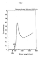
- This method thereby achieves, without directly heating the glass substrate, a polycrystalline silicon thin film having relatively good electrical characteristics such as a high field effect mobility (higher than 100 cm 2 /V ⁇ sec). More specifically, amorphous silicon has a transmissivity characteristic as shown in Fig.
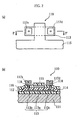
- Figs. 2(a) and 2(b) schematically show a TFT 110 having a coplanar structure.
- Fig. 2(a) is a plan view of the TFT 110
- Fig. 2(b) is a cross sectional view thereof taken along the line P-P' in Fig. 2(a).
- the TFT 110 has an insulating substrate 111 on which there are provided a undercoat layer 112, a p-Si film 113, a first insulating film (gate insulting film) 114, a second insulating film 116, and three electrodes, namely, a gate electrode 115, a source electrode 117s, and a drain electrode 117d.
- the p-Si film 113 is a crystalline semiconductor layer composed of Si (silicon).
- the p-Si film 113 is formed on the undercoat layer 112, patterned in a predetermined shape.
- the p-Si film 113 comprises a channel region 113a, a source region 113b, and a drain region 113c, and the source region 113b and the drain region 113c are disposed on both sides of the channel region 113a.
- the source region 113b and drain region 113c are formed by doping impurity ions such as phosphorus ions and boron ions.
- the first insulating film 114 is made of, for example, silicon dioxide (SiO 2 ), and is formed over the p-Si film 113 and the undercoat layer 112.
- the gate electrode 115 is a metal thin film made of, for example, aluminum (Al) or the like.
- the gate electrode 115 is disposed above the first insulating film 114 at the position corresponding to the channel region 113a of the p-Si film 113.
- the second insulating film 116 is made of, for example, SiO 2 , and stacked above the gate electrode 115 and the first insulating film 114.
- the first insulating film 114 and the second insulating film 116 each have a contact hole 118 formed so as to reach the source region 113b or the drain region 113c in the p-Si film 113. Via the contact hole 118, the source electrode 117s and the drain electrode 117d are in contact with the source region 113b or the drain region 113c. In a region not being the cross section shown in the figure, the gate electrode 115, the source electrode 117s, and the drain electrode 117d are patterned in a predetermined shape to form a wiring pattern.
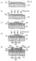
- the TFT 110 is produced in the following manner. First, the undercoat layer 112, made of for example SiO 2 , is formed on the insulating substrate 111. This prevents impurities from diffusing into a p-Si film 133 to be formed Later. Next, on the undercoat layer 112, an a-Si film (not shown) as the foregoing amorphous silicon is deposited by, for example, a plasma CVD method. The a-Si film is then patterned into a predetermined shape by etching. It is noted that the patterning may be performed after the crystallization. Thereafter, the a-Si film is irradiated with an excimer laser having a short wavelength, and cooled (laser annealing).
- an excimer laser having a short wavelength
- the a-Si film is modified, i.e., the a-Si film is polycrystallized to form a p-Si film 113.
- the a-Si film has a large light absorption coefficient in a short wavelength range, and therefore, by employing an excimer laser as the energy beam, it is possible to selectively heat the a-Si film alone. Accordingly, temperature rise of the insulating substrate 111 is suppressed, and this leads to an advantage that low-cost substrates such as glass substrates can be employed for the insulating substrate 111.
- the first insulating film 114 is deposited by an atmospheric pressure CVD (chemical vapor deposition) method, and the gate electrode 115 is formed on the first insulating film 114. Thereafter, using the gate electrode 115 as a mask, impurity ions for serving as either donors or acceptors, specifically, such impurity ions as phosphorus ions and boron ions, are implanted into the p-Si film 113 by using, for example, an ion doping method.
- the channel region 113a, the source region 113b, and the drain region 113c are formed on the p-Si film 113.
- the second insulating film 116 is formed on the gate electrode 115. Thereafter the contact holes 118 are formed, and aluminum, for example, is deposited, and patterning is performed to form the source electrode 117s and the drain electrode 117d.
- the pulsed type laser such as the excimer laser used in the forming process of p-Si films as described above has a large output power, and by irradiating the substrate with the laser light in such a manner that the substrate is scanned by the laser light with a line-like shape while the substrate is being moved, a large-area amorphous silicon can be crystallized at one time, which is an advantage in the large-scale production of semiconductor devices.
- a laser has a drawback that it is difficult to improve quality of the formed crystals.
- a laser of this type has a very short irradiation time for 1 pulse, namely approximately several ten nanoseconds, and causes a large temperature difference between a time during which the irradiation is performed and a time during which the irradiation is not performed is large, and thereby, the fused silicon film crystallizes during the process of being rapidly cooled. Accordingly, the control of a degree of crystal growth and a crystal orientation is difficult, which leads to many drawbacks as follows: sufficient crystal growth tends not to occur, thereby crystal grain sizes are reduced and densities of grain boundaries are increased, uneveness in crystals is increased, and further crystal defects tend to increase.
- crystal nuclei are formed in a disorderly manner, and the disorderly-formed crystal nuclei in turn grow in disorderly directions.
- the crystal growth stops in a state where crystal grains collide with each other.
- the crystal grains formed through such a growth process results in small grains having random shapes. Consequently, in the resulting poly-Si film, a large number of grain boundaries are present and therefore charge carriers cannot transfer smoothly, which causes the film to have poor TFT characteristics such as field effect mobilities.
- the aforesaid excimer laser is generated by exciting a mixed gas containing a rare gas such as Xe and Kr and a halogen such as Cl and F with the use of an electron beam.
- the laser as it is cannot be suitably used.
- the light beam generally used in laser annealing is shaped into a light beam having a homogeneous light intensity and having a line-like shape or a rectangular shape with each line segment being about several centimeters.
- the light beam thus shaped is employed for the technique in the crystallization of non-single crystalline thin films (normally, amorphous thin films), the technique in which the substrate is scanned with the light beam.
- a glass substrate 121 having a precursor semiconductor thin film 122 formed thereon is placed on a substrate stage 124.
- a substrate stage 124 heated at about 400°C by a substrate heater 125, a laser beam 123a of an excimer laser 123 is applied to the precursor semiconductor thin film 122.
- the additional heating of the glass substrate in the irradiation with laser beam achieves high crystal quality, i.e., relatively large and uniform crystal grains, thereby improving the electrical characteristics.
- Technique (1) described above can be employed to obtain a single crystal, whereas technique (2) above is relatively easy to implement and can suppress the variation of field effect mobilities within ⁇ 10%.
- these techniques have the following problems and cannot meet the requirements in recent technical trends towards multi-dimensional integration and further cost reduction.
- technique (1) above requires a step of providing a reflective film etc., which complicates the manufacturing process and adds the manufacturing cost. Furthermore, since providing a reflective film etc. in a narrow, limited space is difficult, crystallization of specific regions with a very small size is accordingly problematic.
- technique (2) involves a step of heating the substrate, which reduces the productivity.
- the step of heating and cooling the substrate takes a long time (30 minutes to 1 hour, for example), which reduces the throughput.
- This problem becomes more serious as a substrate area increases, since a larger substrate requires a longer time for heating and cooling to alleviate the deformation of the substrate.
- this technique can reduce the variation of field effect mobilities to a certain extent, but cannot sufficiently increase the field effect mobilities per se, and therefore it is not suitable for producing circuits in which high speed operation is required. In order not to cause the deformation etc.
- the substrate cannot be heated in excess of 550 °C, and therefore it is difficult to attain further higher crystal quality.
- this technique involves heating the entire substrate, and therefore is not suitable, for the crystallization in a limited region (specific region) on the substrate.
- both techniques (1) and (2) above have problems such as high manufacturing cost.
- techniques (1) and (2) above (including other prior art techniques) have a significant problem of the difficulty in realizing diverse and multi-dimensional layer stacking.
- the methods for controlling the temperature distribution employed by these techniques are not suitable for selectively forming on a single substrate both a circuit region where high speed operation is required (polycrystallized region) and another circuit region where not such high speed is required (amorphous region). For this reason, by these techniques, it is difficult to achieve both a high degree of integration and cost reduction at the same time.
- the polycrystalline thin films of the quality realized by the prior art technique are unsatisfactory.
- the pixel region of LCDs generally requires a mobility of about 0.5-10 cm 2 /Vs
- the peripheral driving circuits for controlling the pixels such as gate circuits and source circuits
- the prior art technique utilizing the light beam having the above-described characteristic cannot achieve high mobilities constantly.
- higher transistor characteristics are attained as the crystal grain size is increased, but the above-described polycrystallization treatment cannot attain sufficient transistor characteristics.
- Fig. 5 schematically shows the distribution of crystallinity in the case where the above-described rectangular light beam is applied to an amorphous silicon thin film formed on a substrate.
- the numeral 1701 refers to the boundary of the irradiation beam
- the numerals 1702 and 1704 refer to the portions where the crystallinity is low
- the shaded portion 1703 indicates the portion where the crystallinity is high.
- the crystallinity shows such a distribution pattern that only the shaded portion 1703 slightly inside the boundary of the irradiation light shows high crystallinity, whereas the crystallinity is low in the other portions (the adjacent portion 1702 to the boundary, and the central portion 1704) show low crystallinity. This has been confirmed by micro-Raman spectroscopy.
- Fig. 6 shows the measurement result of Raman intensity on the portion along the line A-A in Fig. 5.
- the abrupt peaks in Fig. 6 existing slightly inside the boundary indicate that the crystallinities in these portions are high.
- the absence of peaks in the central portion shows that the crystallinity in the central portion is low.
- amorphous silicon thin film is irradiated with a light beam to heat the thin film so that the temperature of the thin film is increased above the melting point temperature of silicon (about 1400 °C or higher), and thereafter the light irradiation is stopped. Thereby, the temperature of the thin film decreases by heat dissipation, and in this process, the fused silicon crystallizes.
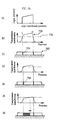
- the surface of the irradiated thin film shows a temperature distribution pattern as in Fig. 7(b).
- the temperature of the amorphous silicon film is increased at a temperature higher than the melting point, and when the amorphous silicon thin film is fused and then solidified in the regions heated above the melting point, crystallization occurs, resulting in polycrystallization. Following this, as the temperature further decreases (Fig. 7(d)), the crystallization further proceeds from the crystal nuclei 1903 as the starting points towards the central portion, where the temperature has not yet reach the crystallization temperature (Fig. 7(e)). In the case of using the light beam having a uniform energy intensity, the temperature decreases in such a manner that no temperature gradient in the surface direction in the central portion is present, as shown in Figs. 7(b), 7(d), and 7(f).
- a relatively wide region reaches the crystallization temperature at one time (Fig. 7(f)), and the crystal nuclei can be formed at any point of the wide region 1904 with an equal probability. Therefore, as shown in Fig. 7(g), micro crystal nuclei are simultaneously formed on the entire surface of the region 1904, and as a result, a poly-Si thin film made of a multiplicity of microcrystal grains is formed. Such a poly-Si thin film inevitably has a large density of grain boundaries. Therefore, the degree of carriers being caught in the grain boundaries increases, reducing the field effect mobility. It is noted that in Fig. 7(c), the numeral 1900 represents a cross section of the thin film.
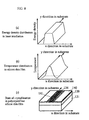
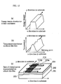
- Fig. 8(a) illustrates the distribution of energy densities in the directions x and y of an excimer laser to be used.
- Fig. 8(b) shows the distribution of the increased temperatures of the amorphous silicon thin film irradiated with the excimer laser having such energy densities.
- Fig. 8(c) is a perspective view of a polycrystalline silicon thin film transistor irradiated with the laser as shown in Figs. 8(a) and 8(b). As seen from these figures, since the laser having such an energy distribution as shown in Fig.
- the region to be irradiated shows a temperature distribution almost uniform along the y direction, but shows such a temperature distribution in the x direction that the central portion is high and both side portions are low, as shown in Fig. 8(b). Due to such a temperature distribution, the crystallization proceeds from the peripheral regions towards the central region along the x direction, and the crystallization growth fronts of the numerous formed crystal nuclei from both peripheral regions meet at the central region. Therefore, as shown in Fig. 8(c) which schematically illustrates the state of the crystallization in the polycrystalline silicon thin film, although the crystal grain size is large in the regions where the line beam energy density of the laser beam is low, the grain size becomes small in the region where the energy density is high (the central region).
- the numeral 131 designates the transparent insulating substrate, the numeral 134 the polycrystal silicone thin film, and the numeral 141 the crystal grains.
- the numeral 139 refers to an insulating film which generally composed of a silicon dioxide (SiO 2 ) film, and the numeral 140 represents the amorphous silicon thin film.
- the numeral 151 designates a laser oscillator
- the numeral 152 a reflector the numeral 153 a homogenizer
- the numeral 154 a window the numeral 155 a substrate having an amorphous silicon layer formed thereon
- the numeral 156 a stage the numeral 157 a control unit.
- the laser annealing apparatus is so constructed that a laser light emitted from the laser oscillator 151 is guided to the homogenizer 153 by the reflector 152, and the laser beam shaped by the homogenizer 153 in a predetermined shape with a uniform energy is applied through the window 154 onto the substrate 155 fixed on the stage 156 in the treatment chamber.
- the regions to be irradiated is in turn staggered so that the region to be irradiated overlaps with the already irradiated region, in order to irradiate the entire substrate surface under the same condition. See for example, I. Asai, N. Kato, M. Fuse, and T. Hamano, Jpn. J. Apl. Phys. 32 (1993) p. 474.
- prior art laser annealing methods have the following drawbacks. Controlling crystal grain sizes and crystal orientations is difficult and thereby forming semiconductor thin films having high crystal quality, i.e., large and uniform crystal grain sizes and few crystal defects. In addition, the reduction in manufacturing cost by increasing throughputs is difficult. Furthermore, prior art methods cannot achieve the improvement in film characteristics of semiconductor thin films (field effect mobilities etc.) and the uniformity of the film quality at the same time.
- crystallization means both single crystallization and polycrystallization, and that a method for producing a crystalline semiconductor thin film according to the present invention is particularly useful in producing poly-Si thin films.
- the present inventors have, as a result of intensive studies, found a method of forming at least a region in which a transistor is formed into a polycrystalline silicon thin film having a large grain size, based on the consideration that a cause of crystal grains in a polycrystalline silicon thin film being undesirably small is a temperature variation in the silicon thin film heated by irradiating with an excimer laser.
- the present inventors have reached the following idea; when performing a polycrystallization treatment by laser, by providing a region having a high thermal conductivity on both sides of the region in which a transistor is formed so as to sandwich the transistor-forming region, the temperature of the peripheral regions sandwiching the transistor-forming region is made higher than the temperature of the transistor-forming region, which makes the temperature of the transistor forming region lower relative to the peripheral regions, and thereby the silicon film in the transistor-forming region is initially crystallized to increase crystal grain sizes.
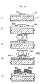
- a method of producing a semiconductor thin film comprising the steps of stacking on a substrate a first insulating film having a first thermal conductivity and a second insulating film having a second thermal conductivity being different from the first thermal conductivity, the second insulating film selectively formed in a partial region on the substrate, stacking a non-single crystal semiconductor thin film over the first insulating film and the second insulating film, and irradiating the non-single crystal semiconductor thin film with an energy beam to effect a crystal growth.
- a thermal conductivity of a region in which a transistor is formed is made different from a thermal conductivity of other regions, and thereby a thermal conductive performance of the amorphous silicon thin film in the region in which a transistor is formed is made higher than that of the amorphous silicon thin film in the other regions.
- the temperature of the silicon thin film in the region where a transistor is formed is lower than that of the other regions, and as a result, crystallization starts from the region in which a transistor is formed. Consequently, a grain size of the polycrystalline silicon in the region in which a transistor is formed can be made large.
- At least a part of a peripheral edge of the semiconductor thin film at least one protruding part extending towards a horizontal direction with respect to the semiconductor film may be provided.
- the present inventors made strenuous efforts in order to discover the cause of the foregoing problems in prior art, and reached the following factors as the cause.
- the generation of crystal nuclei and the crystal growth are effected by heating a semiconductor film by an annealing treatment and thereafter cooling the semiconductor film.
- the semiconductor film is almost uniformly cooled after the annealing treatment regardless of whether it is in the central region or in the peripheral region, and as a result, crystal nuclei start to develop at random positions almost at one time. It is considered that this makes it difficult to control crystal grain sizes and crystal orientations.
- crystal nuclei start to develop at relatively adjacent positions almost at one time and thereby the crystals tend to interfere with each other in the process of crystal growth. This makes it difficult to obtain a sufficient crystal grain size.
- the present inventors have made strenuous studies and reached a technical idea of the present invention that "the formation of crystal nuclei in the peripheral region in the semiconductor film is started earlier than the formation of crystal nuclei in the central region, and thereafter the crystal nuclei formed in the peripheral region are grown towards the central region before crystal nuclei start to form or grow, in order to control crystal grain sizes and crystal orientations and to obtain a sufficient crystal grain size by preventing the crystals undergoing crystal growth from interfering with each other.”
- the heat accumulated in the protruding part in the peripheral edge diffuses in a plurality of outward directions with regard to a horizontal plane (for example, in three directions in the case of the protruding part having a rectangular shape), whereas the heat accumulated in the central region can escape, with regard to a horizontal plane, only in the directions towards the peripheral edge, which has not yet been cooled, and therefore the peripheral edge region, including the protruding part, can be cooled sufficiently earlier than the central region.
- the crystal nuclei in the peripheral edge region start to form earlier than those in the central region, and the crystal nuclei in the peripheral region grow towards the central region before crystal nuclei are formed or grown in the central region, which makes it possible to control crystal grain sizes and crystal orientations. Thereby, it is prevented that the crystals in the process of crystal growth interfere with each other, and a sufficient crystal grain size can be obtained.
- the protruding part may have a size such that one crystal nucleus is formed when crystal growth takes place by irradiating with the energy beam. Accordingly, only one crystal nucleus is formed in the protruding part, and the crystal nucleus is grown to be a crystal.
- a length of said protruding part in a direction of protruding is greater than a film thickness of said semiconductor thin film, and equal to or less than 3 ⁇ m, or a width of the protruding part in a width direction perpendicular to the direction of protruding is greater than the film thickness of the semiconductor thin film, and equal to or less than 3 ⁇ m. Accordingly, the crystal grain size is further finely adjusted, and it is ensured that one crystal nucleus is formed in each protruding part.
- the semiconductor thin film may be formed in a shape having a pair of line segments opposed to each other; two or more of the protruding parts may be formed in each of the pair of line segments; and an interval of the protruding parts next to each other in each of the pair of line segments may be set to be approximately equal to an interval of the opposing line segments.
- the crystal nucleus formed and grown in the protruding part further grows towards the central region, and it is expected that crystal growth is effected such that both the crystals grown from the protruding parts next to each other towards the central region and the crystals grown from the protruding parts in the opposed line segments towards the central region are grown with a minimum interference with each other.
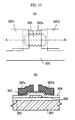
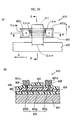
- a semiconductor device comprising a semiconductor thin film wherein crystals are grown by irradiating a non-single crystal semiconductor thin film with an energy beam, characterized in that a protruding part is formed in a peripheral edge region of the semiconductor thin film, the protruding part extending outwardly in the same plane as a plane of the semiconductor thin film.
- a thin film transistor having a source region, a gate region, and a drain region each made of the semiconductor thin film may be formed, and the protruding part may be formed at least in a peripheral edge region of the gate region.
- the protruding part is provided in the region corresponding to the gate electrode, and thereby a good electrical conductivity is obtained.
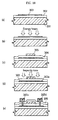
- a method of producing a semiconductor thin film comprising the steps of forming a non-single crystal semiconductor thin film having a protruding part extending outwardly in the same plane as a plane of the non-single crystal semiconductor thin film, and growing crystals in the non-single crystal semiconductor thin film by irradiating with an energy beam.
- crystal nuclei in a peripheral region in the non-single crystal semiconductor thin film are formed earlier than crystal nuclei in a central region in the non-single crystal semiconductor thin film, and thereafter, the crystal nuclei in the peripheral region are grown towards the central region before the crystal nuclei in the central region start to be formed or grown.
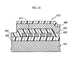
- the present invention also provides a crystalline thin film transistor including a crystalline semiconductor layer formed on a substrate, the crystalline semiconductor layer comprising a channel region, a source region disposed at both sides of the channel region, and a drain region, wherein the crystalline semiconductor layer is such that a non-single crystalline thin film is crystallized, and at least in the channel region in the crystalline semiconductor layer, a gap for controlling an orientation of crystal growth is provided.
- a gap for controlling an orientation of crystal growth formed in the channel region controls an orientation of crystal growth in the channel region when the non-single crystalline thin film is crystallized. Accordingly, in the crystalline semiconductor layer having such a gap for controlling an orientation of crystal growth, shapes and density of grain boundaries of the crystals are preferably controlled, and hence the crystalline thin film transistor exhibits excellent TFT characteristics, such as field-effect mobility.
- the gaps for controlling an orientation of crystal growth is a depressed part formed on the surface of crystalline semiconductor layer (non-single crystalline thin film in the process of fabrication), and the depressed part may extend to a lower layer under the crystalline semiconductor layer (the surface of the substrate or the undercoat layer) or may not extend to the lower layer.
- the sizes and shapes thereof are not particularly restricted, and therefore may be suitably adjusted depending on the surface area and thickness of the crystalline semiconductor layer, a desired field effect mobility, and so forth.
- Examples of the surface shapes thereof include a circular shape, a square-shaped hole, a long and narrow groove, and so forth, and examples of the cross-sectional shape thereof include a C-like shape, a V-like shape, and an angular C-like shape.
- the detail of the gap for controlling an orientation of crystal growth will be described later.
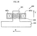
- a crystalline thin film transistor including a crystalline semiconductor layer formed on a substrate, the crystalline semiconductor layer comprising a channel region, a source region disposed at both sides of the channel region, and a drain region, wherein the crystalline semiconductor layer is such that a non-single crystalline thin film is crystallized, wherein the gap for controlling an orientation of crystal growth is divided into two or more arrays of groove-like gaps provided in a direction linking the source region and the drain region.
- two or more arrays of groove-like gaps functions so that the orientation of crystal growth is guided in the direction linking the source region and the drain region, and the resulting poly-Si film becomes an aggregate of large crystal grains longitudinally extending in the direction linking the source region and the drain region.
- Such a poly-Si film has a small density of grain boundaries in the direction linking the source region and the drain region and therefore exhibits a high carrier mobility.
- the crystalline thin film transistor having the above-described configuration has excellent characteristics such as carrier mobilities.
- non-single crystalline thin film which is a precursor material of the crystalline semiconductor layer
- two or more arrays of groove-like gaps for controlling an orientation of crystal growth (denoted by the reference numeral 411) are formed in the direction linking the source region and the drain region, and thereafter an energy beam capable of being absorbed is applied to the thin film in a conventional manner.
- the resulting temperature distribution on the surface of the thin film is as follows; the gaps for controlling, the region adjacent thereto, and the peripheral edge region show a low temperature, and the main portion of the channel region (a region of the thin film where the gap for controlling an orientation of crystal growth is not formed) shows a high temperature.
- the groove region (gaps for controlling an orientation of crystal growth) has a smaller film thickness than the other regions or has no thin film thereon, less energy beam is absorbed in the groove region, and as a result the temperature of the groove region becomes lower than the other regions.
- the temperature of the peripheral edge region becomes lower than the central region of the thin film.
- Figs. 11(a) and 11(b) schematically illustrate a state of the crystal growth.
- crystal nuclei are formed in a peripheral region of the gap for controlling an orientation of crystal growth, where the temperature is lower than that of the main portion.
- the crystal nuclei grow in a direction towards a region having a higher temperature, i.e., in a direction away from the groove-like gap for controlling an orientation of crystal growth (a perpendicular direction to the groove), as the temperature of the whole thin film falls.
- two or more array of the gaps for controlling an orientation of crystal growth are provided in the direction linking the source region and the drain region, and therefore, the crystal nuclei formed in the regions adjacent to the two gaps an orientation of crystal growth opposed to each other grow towards the center of the main portion of the channel region from the opposite directions. Therefore, both crystal grains collide with each other in the vicinity of the center of the main portion of the channel region.
- the central region being far from the gap for controlling an orientation of crystal growth, has still a higher temperature than the other regions and therefore is in a state where molecules therein can still freely move.
- the orientation of crystal growth is guided to the direction in which the collision is avoided, i.e., the direction linking the source region and the drain region (the direction parallel to the groove, see Fig. 11a).
- a large crystal grain is formed so as to longitudinally extend in the direction linking the source region and the drain region (see Fig. 11b).
- the channel region is composed of an aggregate of the crystal grains having such a shape, the density of grain boundaries in the direction linking the source region and the drain region becomes small, and therefore a crystalline thin film transistor having excellent TFT characteristics such as field effect mobility can be formed.
- the gap for controlling an orientation of crystal growth may be divided into a plurality of gaps discontinuously provided in a direction linking the source region and the drain region.
- crystal nuclei are formed in the vicinity of the gap for controlling an orientation of crystal growth, in which the temperature decreases to a crystallization temperature earlier.
- the intervals between the crystal nuclei are narrow, the crystal growth is hindered since crystals collide with other crystals before they sufficiently grow, and this results in a polycrystal made of a multiplicity of micro-crystal grains and a distorted crystal structure in the vicinity of the boundaries where crystal grains collide with each other. For this reason, desired TFT characteristics cannot be obtained. Accordingly, in order to improve TFT characteristics such as field effect mobility, it is necessary that the density of crystal nuclei to be formed should be appropriately controlled, in addition to the control of the orientation of crystal growth.
- the gaps are arranged in a discontinuous manner, although crystal nuclei are formed in the vicinity of the gaps, they are not easily formed in intermediate regions between a gap and the next gap.
- the density of crystal nuclei to be formed can be controlled. It is noted that the reason why crystal nuclei are not easily formed in the intermediate region between a gap and the next gap is that the intermediate region (the region where the thin film material is present) is sufficiently heated by laser irradiation.
- a semiconductor device including a crystalline semiconductor layer formed on a substrate, the crystalline semiconductor layer comprising a channel region, a source region disposed at both sides of the channel region, and a drain region, the semiconductor device wherein the crystalline semiconductor layer is such that a non-single crystalline thin film is crystallized and at least in the channel region, an early-crystallization region in which a crystallization-starting temperature is higher than that in a main portion of the channel region is provided.
- the early-crystallization region serves to control the crystal growth in the main portion of the channel region, and as a result, high quality crystalline semiconductor layer having a small density of grain boundaries can be formed.
- the reason is as follows.
- crystal nuclei start to be formed earliest in the early-crystallization region.
- the crystal nuclei become the center of the crystal growth to take place thereafter. Accordingly, by providing the early-crystallization region, the phenomenon that multiple crystal nuclei are formed at once can be prevented, and as a result, a polycrystalline semiconductor layer in which large crystal grains are aggregated can be formed.
- the early-crystallization region be arranged at least one or more in the channel region, and it is also preferable that a plurality of early-crystallization regions be provided at positions where the transfer of carriers in the direction linking is not hindered.
- a plurality of early-crystallization regions are provided on the surface of the thin film at appropriate positions and intervals, the density of crystal nuclei to be formed can be appropriately controlled, resulting in further desirable results.
- a crystallization-starting temperature is high means that crystallization starts to take place at a higher temperature than that in the main portion of the channel region.
- the early-crystallization region has a shape longitudinally extending in a direction linking the source region and the drain region.
- the region is preferable to have a narrow width in the direction linking the source region and the drain region. If the early-crystallization region extends longitudinally in the direction linking the source region and the drain region, the early-crystallization region can become a factor that hinders carrier mobilities.
- the early-crystallization region is such that an impurity is contained in a component constituting the main portion of the channel region.
- the crystalline thin film transistor having the above-described configuration not only exhibits excellent TFT characteristics such as field effect mobility but also achieves a reduced cost.
- the crystalline semiconductor layer is substantially composed of silicon or a compound of silicon and germanium.
- Silicon and a compound of silicon and germanium are readily available and easy to crystallize. Accordingly, the above-described configuration achieves a high quality crystalline thin film transistor at a low cost.
- a method of producing a crystalline thin film transistor including a crystalline semiconductor layer, the crystalline semiconductor layer comprising a channel region, a source region disposed at both sides of the channel region, and a drain region, the method comprising at least the steps of depositing a non-single crystalline thin film on an insulating substrate, forming a plurality of gaps for controlling an orientation of crystal growth in the non-single crystalline thin film, and irradiating the thin film in which the plurality of gaps are formed with an energy beam to crystallize the thin film.
- the gaps for controlling an orientation of crystal growth may be formed in a direction linking the source region and the drain region so as to have a groove-like shape, and in addition, the gap for controlling an orientation of crystal growth may be divided into a plurality of gaps discontinuously formed in a direction linking the source region and the drain region.
- a method of producing a crystalline thin film transistor including a crystalline semiconductor layer, the crystalline semiconductor layer comprising a channel region, a source region disposed at both sides of the channel region, and a drain region, the method comprising at least the steps of; depositing a non-single crystalline thin film on an insulating substrate, forming an early-crystallization region by ion-implanting an impurity in a partial region in the non-single crystalline semiconductor thin film, the impurity for raising a crystallization-starting temperature of the partial region, and after the step of forming an early-crystallization region, irradiating the thin film with an energy beam to crystallize the thin film.
- the early-crystallization region may have a belt-like shape longitudinally extending in a direction linking the source region and the drain region, and in addition, the early-crystallization region is divided into a plurality of early-crystallization regions discontinuously disposed in a direction linking the source region and the drain region.
- the energy beam may be an excimer laser beam.
- Excimer lasers have a large light energy and is well absorbed by silicon since they are UV lights. Therefore, by using an excimer laser beam, crystallization of the non-single crystalline semiconductor layer can be efficiently performed.
- the non-single crystalline semiconductor layer is composed of a material capable of absorbing ultraviolet rays such as silicon, it is possible to selectively heat and fuse only the semiconductor layer. Therefore, the crystallization of the semiconductor layer can be effected without causing adverse effects by heat on the regions not irradiated with the beam, and moreover, it is made possible to employ glass substrates, which are low in cost.
- the temperature difference between the gap for controlling an orientation of crystal growth and the main portion of the semiconductor layer becomes large, and thereby the function of the gap for controlling an orientation of crystal growth (function for controlling the orientation of crystal growth) can be fully exploited.
- the present inventors have also carried out a study on methods for sufficiently growing crystals based on the foregoing considerations regarding the mechanism of crystallization. As a consequence, the inventors have found that by intentionally making uneven a distribution of the light intensity within the light beam width, crystallization can smoothly progress, and thereby a high quality crystalline thin film can be obtained. Based on this view, the following aspects of the present invention have been accomplished.
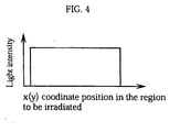
- a method of producing a semiconductor device wherein a thin film of a non-single crystalline material formed on a substrate is irradiated with a light beam whereby the non-single crystalline material is crystallized or recrystallized to form a crystalline semiconductor thin film, the method characterized in that the light beam is such that a distribution pattern of a light energy intensity of the light beam is adjusted so that a temperature gradient or an uneveness of temperature distribution is caused, and the light beam is applied in a stationary state.
- a distribution pattern of the light energy intensity may be such a distribution pattern that a light intensity within a beam width monotonously increases from one side to the other, or monotonously decreases from one side to the other.
- the temperature gradient on the surface of the non-single crystalline thin film to be irradiated is formed correspondingly to the light energy intensity, and the crystallization is guided in a direction from a region where the temperature is low towards a region where the temperature is high.
- disorderly formation of crystal nuclei and disorderly crystal growth are prevented, and consequently it is ensured that the phenomenon explained with Figs. 7(f) and 7(g) is prevented.
- the crystalline thin film for, for example, a semiconductor circuit comprising a source region - a channel region - and a drain region
- the intensity gradient of the light energy be formed in the direction parallel to the source-drain direction.
- the direction of crystal growth is restricted to the direction parallel to the direction of the transfer of carriers, and the density of grain boundaries becomes small. Accordingly, by employing this technique, a mobility of, for example, 300 cm 2 /Vs or higher can be achieved.
- a distribution pattern of the light energy intensity may be such that, in a beam width, a part having a relatively stronger light intensity and a part having a relatively weaker light intensity are alternately arrayed in a plane.
- a striped temperature distribution pattern made of a part having a high temperature and a part having a low temperature is formed on the irradiated surface.
- crystal growth is guided in the direction from a region where the temperature is low (normally formed in a belt-like shape) towards a region where the temperature is high. Then, crystal grains collide with each other in the vicinity of the center of the region (belt) where the temperature is high, forming a continuous line of grain boundaries (a continuous line like a mountain range) there, and crystal grains are formed so as to longitudinally extending in the direction parallel to the continuous line.
- a distribution pattern of the light energy intensity may be formed by causing a light interference by simultaneously irradiating with at least two coherent lights.
- this method utilizing a light interference, it is possible to form a fine light intensity distribution, and as a result to form a fine striped temperature distribution on the surface to be irradiated. Accordingly, this method achieves a smooth crystallization in a relatively wide region.
- a distribution pattern of the light energy intensity of may be a wave-motion-like interference pattern formed by simultaneously irradiating with at least two coherent lights and by dynamically modulating a phase of at lease one of the two coherent lights.
- the energy intensity distribution of the light beam varies in a wave-motion-like manner, and the temperature of the irradiated surface correspondingly varies in a wave-motion-like manner so that the temperature moves in one direction. Accordingly, by employing this method, impurities contained in the non-crystalline thin film can be gradually expelled outside the effective area, and consequently a crystalline thin film having a high purity and a high mobility can be formed.
- the light beam may be applied as the beam is being moved relative to the non-single crystalline thin film on the substrate.
- the light beam having a light energy intensity distribution pattern being adjusted so that a temperature gradient or an uneveness of the temperature distribution is caused on the surface to be irradiated (the surface of the non-single crystalline thin film), the orientation of crystal growth can be finely guided. Therefore, a high quality crystalline thin film having a high uniformity in the degree of crystallinity and a small density of grain boundaries can be obtained.
- a method of producing a semiconductor thin film wherein a thin film comprising a non-single crystalline material formed on a substrate is irradiated with a light beam and thereafter cooled whereby the non-single crystalline material is crystallized or recrystallized, the method characterized in that a pressure of an atmosphere gas is maintained at more than a predetermined value to cause an uneven temperature distribution on a surface of the thin film irradiated with the light beam.
- the pressure of the atmosphere gas to be maintained at more than a predetermined value may be 10 -5 torr or higher where the atmosphere gas is a hydrogen gas.
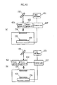
- the invention also provides a method of producing a semiconductor film comprising the step of crystallizing a precursor semiconductor film, the step wherein the precursor semiconductor film formed on a substrate is irradiated with a first energy beam supplying the precursor semiconductor film with at least such an energy that the precursor semiconductor film can be crystallized, and with a second energy beam such that an absorption index of said precursor semiconductor film is smaller than an absorption index by said first energy beam and an energy supplied by said second energy beam is smaller than an energy capable of crystallizing said precursor semiconductor film.
- the second energy beam can easily reach a lower portion of the precursor semiconductor film and further the substrate.
- the precursor semiconductor film is heated through the thickness direction and the substrate is also heated, reducing the temperature difference between the point while the first energy beam is being applied and the point after the irradiation with the beam is completed.
- the precursor semiconductor film heated and fused by being irradiated with the first energy beam is crystallized after the irradiation is completed, while being annealed. Therefore, the crystal growth is facilitated, and it is made possible to form relatively large crystal grains and reduce crystal defects, which improves electrical characteristics of the semiconductor film.
- the precursor semiconductor film may be an amorphous silicon thin film.
- the first energy beam may be such that an absorption coefficient of the precursor semiconductor film is approximately equal to or greater than the reciprocal of a film thickness of the precursor semiconductor film
- the second energy beam may be such that an absorption coefficient of the precursor semiconductor film is approximately equal to or less than the reciprocal of a film thickness of the precursor semiconductor film
- the first energy beam may be such that an absorption coefficient of the precursor semiconductor film is approximately 10 times or greater than the reciprocal of a film thickness of the precursor semiconductor film
- the second energy beam may be such that an absorption coefficient of the precursor semiconductor film is approximately the reciprocal of a film thickness of the precursor semiconductor film.
- the precursor semiconductor film can be more efficiently heated, and a semiconductor film having further higher quality can be formed.
- the first and second energy beams have a different wavelength from each other.
- the foregoing energy beams having a different wavelength from each other may be, for example, such that the first energy beam is an energy beam having a single wavelength, and the second energy beam includes at least a wavelength component in a visible light range.
- the first energy beam and the second energy beam may be, for example, a laser light and an infrared lamp, a laser light and an incandescent light, or a laser light and an excimer lamp light.
- the second energy beam may contain at least a wavelength component from a visible light range to an ultraviolet range, such as a xenon flash lamp light.
- first energy beam and the second energy beam may be a laser light.
- the irradiation with the energy beam having a large energy density can be readily performed, and thereby it is made easy to efficiently heat the precursor semiconductor film and the substrate.
- the first energy beam may be one laser light selected from an argon fluoride excimer laser, a krypton fluoride excimer laser, a xenon chloride excimer laser, and a xenon fluoride excimer laser
- the second energy beam may be a laser light of an argon laser
- the first energy beam is one laser light selected from an argon fluoride excimer laser, a krypton fluoride excimer laser, a xenon chloride excimer laser, and a xenon fluoride excimer laser
- the second energy beam is a laser light of a carbon dioxide gas laser
- Each of the excimer lasers mentioned above is easy to obtain a large power and is easily absorbed in the vicinity of the surface of the amorphous silicon thin film.
- the laser light of an argon laser transmits through the amorphous silicon film to a certain degree and is easily absorbed throughout the thickness direction of the amorphous silicon thin film.
- the carbon dioxide gas laser transmits through the amorphous silicon thin film relatively well and is easily absorbed by the glass substrate. Hence, the amorphous silicon thin film can be efficiently heated, a polysilicon thin film having good crystal quality can be readily formed, and the productivity can be readily improved.
- the first energy beam and the second energy beam may be applied to a belt-like shaped region in the precursor semiconductor film.
- heating can be performed with a uniform temperature distribution, and thereby it is made possible to easily form a semiconductor film having a uniform crystal quality and to reduce the time required for the process of crystallization.
- a region in the precursor semiconductor film to be irradiated with the second energy beam may be larger than a region in the precursor semiconductor film to be irradiated with the first energy beam, and may include the region to be irradiated with the first energy beam.
- heating can be performed with a uniform temperature distribution, and thereby it is made possible to easily form a semiconductor film having a uniform crystal quality.
- the first energy beam and the second energy beam are incident approximately perpendicular to the precursor semiconductor film.
- the second energy beam is applied at least prior to applying the first energy beam.
- Such applying of the second energy beam prior to applying the first energy beam may be performed by controlling the timings of applying of the energy beams, and further, may be performed in such a manner that the substrate on which the precursor semiconductor film is formed is moved, and the second energy beam is applied to a more forward position in the precursor semiconductor film with respect to a direction of moving of the substrate than a position where the first energy beam is applied.
- crystallization is effected by the first energy beam in a state where the semiconductor film and the substrate are sufficiently heated by the second energy beam, resulting in an efficient crystallization process.
- the first energy beam may be intermittently applied, and the second energy beam may be continuously applied.
- the first energy beam may be a pulsed laser light
- the second energy beam may be a continuous-wave laser light or a lamp light.
- the first energy beam and the second energy beam may be synchronized with each other and intermittently applied.
- a time of irradiating with the first energy beam should be within a time of irradiating with the second energy beam, and should be two-thirds or shorter of an irradiation cycle of the second energy beam.
- the first energy beam may be a pulsed laser light
- the second energy beam may be a pulsed laser light or an intermittently-operated lamp light.
- the pulsed laser can easily attain a large power and thereby readily heat a large area at a high temperature. Therefore, the time required for the step of crystallization can be easily reduced to improve productivity.
- the first energy beam and the second energy beam may be applied so that the precursor semiconductor film is heated at a temperature of 300 °C to 1200 °C, or more preferably at a temperature of 600 °C to 1100 °C.
- the temperature variation in crystallization is made gentle and the crystal growth is facilitated while preventing crystal defects and uneven crystallization caused by the formation of micro-crystals in a partial region, and the formation of large crystal grains are readily made possible.
- the method according to this aspect of the invention may further comprise a step of heating the substrate on which the precursor semiconductor film is formed with a heater. More specifically, for example, it is preferable that the substrate on which the precursor semiconductor film is formed should be heated at a temperature of 300 °C to 600 °C.
- the precursor semiconductor substrate is more efficiently heated, and in addition, the crystal growth is readily facilitated by annealing. Moreover, in comparison with the conventional case of heating the substrate with the heater only, a predetermined heating temperature can be obtained within a shorter time, which easily achieves an improvement in productivity.
- the first energy beam may be applied to a plurality of regions in the precursor semiconductor film, and the second energy beam may be applied to only a part of the plurality of regions.
- crystallinity can be improved in a limited region, for example, which requires particularly high electrical characteristics, and therefore a necessary and sufficient crystallization can be effected by a crystallization process with a short time, which easily achieves an improvement in productivity.
- the second energy beam may be such that an absorption index of the substrate is larger than an absorption index of the precursor semiconductor film.
- the first energy beam be such that an absorption coefficient of the precursor semiconductor film is approximately 10 times or greater than the reciprocal of a film thickness of the precursor semiconductor film.
- the precursor semiconductor film is an amorphous silicon thin film
- the first energy beam may be one laser light selected from an argon fluoride excimer laser, a krypton fluoride excimer laser, a xenon chloride excimer laser, and a xenon fluoride excimer laser
- the second energy beam may be a laser light of a carbon dioxide gas laser.
- an apparatus for producing a semiconductor film by crystallizing a precursor semiconductor film formed on a substrate comprising a first irradiating means emitting a first energy beam, and a second irradiating means emitting a second energy beam resulting in a smaller absorption index of said precursor semiconductor film than said first energy beam.
- the second energy beam can easily reach a lower portion of the precursor semiconductor film and further the substrate.
- the precursor semiconductor film is heated through the thickness direction and the substrate is also heated, reducing the temperature difference between the point while the first energy beam is being applied and the point after the irradiation with the beam is completed.
- the precursor semiconductor film heated and fused by being irradiated with the first energy beam is crystallized after the irradiation is completed, while being annealed. Therefore, the crystal growth is facilitated, and it is made possible to form relatively large crystal grains and reduce crystal defects, which improves electrical characteristics of the semiconductor film.
- the second irradiating means is a lamp radially emitting the second energy beam
- the apparatus further comprises a concave reflector collecting the second energy beam.
- the above-described apparatus for producing a semiconductor film may further comprise a reflective plate in which one of the first energy beam and the second energy beam is reflected and the other one of the first energy beam and the second energy beam is allowed to transmit, the apparatus wherein the first energy beam and the second energy beam are incident perpendicular to the precursor semiconductor film.
- the first irradiating means may be one of an argon fluoride excimer laser, a krypton fluoride excimer laser, a xenon chloride excimer laser, and a xenon fluoride excimer laser
- the second irradiating means may be an argon laser
- the first energy beam may be one laser light selected from an argon fluoride excimer laser, a krypton fluoride excimer laser, a xenon chloride excimer laser, and a xenon fluoride excimer laser
- the second energy beam may be a laser light of a carbon dioxide gas laser
- the present invention also provides, in another aspect of the invention, a method of producing a semiconductor thin film comprising a step of irradiating a non-single crystal semiconductor thin film with an energy beam, said non-single crystal semiconductor thin film formed on a substrate having an image display region and a driving circuit region, said method characterized in that a first irradiation of said image display region is performed by using an energy beam having a line-like cross-sectional shape, and a second irradiation of said driving circuit region is performed at a higher energy density than said first irradiation by using an energy beam having a square-like cross-sectional shape.
- the present invention also provides a method of producing a semiconductor thin film comprising a step of irradiating a non-single crystal semiconductor thin film with an energy beam, said non-single crystal semiconductor thin film formed on a substrate having an image display region and a driving circuit region, said method characterized in that a first irradiation of said image display region is a scanning irradiation such that said substrate is scanned by said energy beam in a relative manner and a region to be irradiated with said energy beam is shifted with a predetermined overlap, and a second irradiation of said driving circuit region is a stationary irradiation with a higher energy density than said first irradiation such that said energy beam is fixed with respect to said substrate in a relative manner.
- the thin film transistors constituting a liquid crystal display device different laser irradiation methods are employed for a pixel region which requires a uniformity of semiconductor film characteristics and for a driving circuit region which requires characteristics (particularly high mobility).
- a laser annealing in which amorphous silicon is irradiated with a laser light so as to fuse and crystallize the amorphous silicon to form polycrystalline silicon, the energy density of the laser light applied to the driving circuit region in the substrate plane is made higher than the energy density of the laser light applied to the pixel region, so as to form polycrystalline silicons in the driving circuit region and in the pixel region each having different characteristics from each other.
- a first laser light irradiation is performed for the pixel region alone or for the entire surface of the substrate, and thereafter a second laser light irradiation is performed for the driving circuit region using a laser light having a higher energy density than the laser light used in the first laser light irradiation.
- the mobility of the polycrystalline silicon in the driving circuit region becomes higher than the mobility of the polycrystalline silicon in the pixel region, and the characteristics of the polycrystalline silicon in the pixel region can be made uniform in the plane.
- the first irradiation may be performed by using an energy beam having a line-like cross-sectional shape
- the second irradiation may be performed by using an energy beam having a square-like cross-sectional shape.
- the first irradiation may be a scanning irradiation such that a laser beam is applied a plurality of times while a position to be irradiated with the laser beam is being shifted
- the second irradiation may be a stationary irradiation such that the position to be irradiated is fixed.
- the laser annealing may be performed in such a manner that a plurality of regions in the driving circuit region are irradiated with laser lights having different energy densities from each other, thereby forming poLycrystalline silicons having different characteristics from each other.
- the laser annealing it is preferable that the laser annealing be performed so that a region in which a transfer gate in the latch or shift resistor and the other regions are respectively irradiated with laser lights having different energy densities.
- the edge of the laser beam not fall on the TFT pattern.
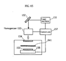
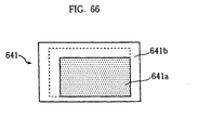
- an apparatus for producing a semiconductor thin film comprising an energy beam generating means, and means for homogenizing an energy beam emitted from the energy beam generating means by shaping the energy beam so as to have a predetermined cross-sectional beam shape and a homogeneous energy, the apparatus wherein a non-single crystal semiconductor thin film formed on a substrate is irradiated with the energy beam to effect crystal growth the apparatus characterized in that the apparatus further comprises a filter having a plurality of transmissivities different from each other, and the energy beam is applied through the filter to a plurality of regions in the non-single crystal semiconductor thin film in such a manner that each of the plurality of regions receives a different energy density from each other.
- the apparatus may be a laser annealing apparatus in which transmissivities of the mask are varied by an optical thin film so as to have the plurality of transmissivities different from each other, and this enables the distribution of transmissivities to accurately formed.
- the apparatus may be a laser annealing apparatus in which the mask and the window for applying the laser light to the substrate in the treatment chamber are integrated, and this enables the apparatus to have a simple construction and to reduce attenuation of the light energy.
- an apparatus for producing a semiconductor thin film comprising an energy beam generating means, and means for homogenizing an energy beam emitted from the energy beam generating means by shaping the energy beam so as to have a predetermined cross-sectional beam shape and a homogeneous energy, the apparatus wherein a non-single crystal semiconductor thin film formed on a substrate is irradiated with the energy beam to effect crystal growth, the apparatus characterized in that, the means for homogenizing is capable of selectively shaping the energy beam into a plurality of cross-sectional beam shapes.
- Figs. 12(a) to 12(c) detailed below is an example in which crystal growth is controlled by providing on a substrate a plurality of regions each having a different thermal conductivity and thereby allowing a semiconductor thin film to have a temperature distribution.
- a lower insulating film 202 is formed on the entire region of a transparent insulating substrate 201 composed of, for example, a glass substrate.
- a stripe-like shaped upper insulating film 203 is formed on a part of the lower insulating film 202.
- the upper insulating film 203 is composed of a material having a smaller thermal conductivity than the lower insulating film 203.
- an amorphous silicon thin film 204 is formed on the lower insulating film 202 and the upper insulating film 203.
- a polycrystalline silicon thin film 210 is formed.
- the thermal conductivity of the upper insulating film 203 is lower than that of the lower insulating film 202, the temperature of a region in the amorphous silicon thin film 204 over the upper insulating film 203 becomes higher than the temperature of a region in the amorphous silicon thin film 204 over an interval of the upper insulating films 203, as shown in Fig. 12(b).
- the crystallization of the amorphous silicon thin film 204 starts from the region over the interval of the upper insulating films 203, and the crystal growth proceeds towards the regions over the upper insulating films 203.
- a collision of the crystal grains each other rarely occurs, and a large crystal grain region 210b in which crystal grains are relatively large is thereby formed.
- each of the crystal grains grown from both sides of the upper insulating films 203 collides with each other, and consequently a small crystal grain region 210a is formed.
- the polycrystalline silicon thin film 210 of the present example employs a silicon nitride thin film having a thickness of 200 nm (thermal conductivity: 0.19 W/cm ⁇ °C) as the lower insulating film 202 and a silicon oxide thin film having a thickness of 30 nm and a width of approx. 5 ⁇ m (thermal conductivity; 0.014 W/cm ⁇ °C) as the upper insulating film 203 with an interval between each of the upper insulating films 203 being 20 ⁇ m.
- the prior art polycrystalline silicon thin film employs a single layer of a silicon oxide thin film having a thickness of 200 nm.
- the thickness of the amorphous silicon thin film was made to be 85 nm.
- the measuring points of the Raman peak strengths were the central region of the region to be irradiated along an x direction in Figs. 12(a) to 12(c).
- the degree of crystallinity is relatively small over the entire region.
- the degree of crystallinity is small in the regions over the upper insulating film 203, which are denoted by A, B, and C in the figure, the regions over the lower insulating film 202 sandwiched by the upper insulating films 203 show large Raman peak strengths. This indicates that the degree of crystallinity is remarkably improved by the method according to the present invention.
- the optimal value for the interval between each of the stripe-like shaped upper insulating films 203 varies depending upon thermal conductivities of the lower insulating film 202 and the upper insulating film 203, energy densities of the light to be irradiated, and so forth.
- the description above shows an example in which the surface of the silicon thin film has a temperature distribution with respect to the y direction in Figs. 12(a) to 12(c).
- the temperature distribution may be also given with respect to the x direction in like manner.
- the influence by the sequential movement of the region to be irradiated on the temperature distribution should be taken into consideration.
- an adjustment of the temperature distribution may be performed by varying an energy density distribution in each of the regions.
- the thermal conductivity of the upper insulating film 203 is made smaller than the thermal conductivity of the lower insulating film 202, so as to increase the grain size in the regions under which the upper insulating film 203 is absent.
- the thermal conductivity of the upper insulating film may be made larger than the thermal conductivity of the lower insulating film, thereby to increase the grain size in the regions under which the upper insulating film is present.
- the former method can more readily increase an area of the region in which the thermal conductivity is high, i.e., the surface temperature of the silicon thin film is low, therefore can more readily increase the temperature gradient in the temperature distribution on the surface of the silicon.
- the relationship between a stacking order and thermal conductivities of the insulating films is not limited to the manner described above, but may be the reverse order, insofar as a predetermined temperature distribution is attained.
- the upper insulating film can be easily formed into a desired shape (thickness) by setting an etching selective ratio (a ratio of etching rates) between the upper insulating film and the lower insulating film. Therefore, the upper insulating film can be made to have a uniform thickness over a wide area, and as a result, a polycrystalline silicon thin film having a uniform grain size in the entire surface of the substrate can be readily obtained.
- a thickness of the silicon thin film may be varied by etching or the like method.
- etching or the like method By employing this method, although relatively high accuracy is needed in the etching, the manufacturing steps can be simplified since forming two layers of insulating films becomes unnecessary.
- the temperature distribution can be provided by forming a plurality of regions each having a different thermal capacity. This can also improve crystallinity of the silicon thin film.
- Example 1-2 describes an example of a polycrystalline silicon thin film transistor employing the semiconductor thin film made in accordance with the foregoing example.
- Fig. 14(a) shows a plan view of the polycrystalline silicon thin film transistor
- Fig. 14(b) shows a cross section taken along the line A-A' in Fig. 14(a).
- a transparent insulating substrate 201 there are shown a transparent insulating substrate 201, a lower insulating film 202, a upper insulating film 203, a gate insulating film 205, a source electrode film 206, a drain electrode film 207, a gate electrode film 208, and a large crystal grain region 210b in a polycrystalline silicon thin film 210.
- the polycrystalline silicon thin film 210 is polycrystallized in the manner described in the above Example 1-1.
- the large crystal grain region 210b sandwiched by the upper insulating films 203 is selectively left unremoved by etching or the like method, and a source-drain direction is made to be in parallel with a direction of a stripe-like pattern formed by the upper insulation films 203.
- the gate insulating film 205, the source electrode film 206, the drain electrode film 207, and the gate electrode film 208 can be formed by the same methods as used for forming conventional thin film transistors, such as a thin film deposition and a patterning
- the polycrystalline thin film transistor thus obtained exhibited a field effect mobility of approximately 180 cm 2 /V ⁇ sec, whereas a transistor made in accordance with a prior art method showed a field effect mobility of 70 cm 2 /V ⁇ sec, which demonstrates that a remarkable improvement in TFT characteristics was achieved.
- the relationship between the direction of the upper insulating film 203 and the source-drain direction is not limited to the above-described relationship, in which both are directed to the same direction. Many variations are possible insofar as the source-drain direction is made to be in the lengthwise direction of the crystal grains formed according to the interval between each of the upper insulating films 203 and so forth.
- Example 1-3 describes an example in which a polycrystalline silicon thin film transistor having a larger size than the transistor produced in accordance with the foregoing Example 1-2.
- a polycrystalline silicon thin film transistor of Example 1-3 differs from the thin film transistor of the foregoing Example 1-2 in that two large crystal grain regions 210b formed between three upper insulating films 203 are employed to form the transistor.
- a silicon oxynitride thin film formed by a plasma CVD having a thickness of approximately 200 nm is used for the lower insulating film 202
- a silicon oxide thin film having a thickness of approximately 40 nm is used for the upper insulating films 203.
- Each of the large crystal grain regions 210b is formed by firstly forming an amorphous silicon thin film 204 having a thickness of 85 nm on the upper insulating film 203 formed by pattering, and then irradiating the amorphous silicon thin film 204 with an excimer laser as in Example 1-1 to obtain a polycrystalline silicon thin film.
- the temperature gradient is deliberately increased instead of increasing the interval of the upper insulating films 203, and a plurality of large crystal grain regions 210b with a desirable crystal condition are formed.
- a material for the insulating film to be formed on the transparent insulating substrate is not limited to silicon nitride, silicon oxynitride, and silicon oxide. Other materials may be employed insofar as the materials have different thermal conductivities from each other and a selective etching for the materials is possible.
- Example 2-1 As a semiconductor device of Example 2-1, an example of a thin film transistor as a semiconductor device having large crystal grains is described below.
- Figs. 16(a) and 16(b) show schematic views of a thin film transistor.
- Fig. 16(a) shows a plan view thereof
- Fig. 16(b) shows a cross sectional view taken along the line A-A' in Fig. 16(a).
- an insulating substrate 301 is shown.
- an undercoat layer 302 is provided, and on the undercoat layer 302, a semiconductor layer 303 is formed by crystallizing an amorphous semiconductor film.
- a semiconductor layer 303 is formed by crystallizing an amorphous semiconductor film.
- a plurality of protruding parts 303a are formed with predetermined intervals, and each of the protruding parts 303a extends outwardly in the same plane as that of the semiconductor layer 303.
- Each protruding part 303a is so formed as to have an approximately rectangular shape, and the length (a length of a line protruding from the semiconductor layer 303) and the width (a length of a line perpendicular to the line protruding from the semiconductor layer 303) are made to be 1 ⁇ m.
- a first insulating layer 304 is provided over the semiconductor layer 303 so as to cover the semiconductor layer 303, and a gate electrode 305 as a first electrode is provided at a predetermined position on the first insulating layer 304.
- a second insulating layer 306 is provided so as to cover the gate electrode 305, and a source electrode 307s and a drain electrode 307d are provided at a predetermined position on the second insulating layer 306, as a pair of second electrodes electrically connected with the semiconductor layer 303.
- the width of the protruding part 303a is not limited to 1 ⁇ m. However, in order to provide one crystal nucleus for each of the protruding parts 303a, it is preferable to make the width within the range of from a width approximately equal to or greater than the thickness of the semiconductor layer 303 (for example, 0.05 ⁇ m) to approximately 3 ⁇ m.
- the width of the protruding part 303a is smaller than the thickness of the semiconductor layer, there is a possibility that the crystal nucleus to be grown in the protruding part 303a is dragged into the semiconductor layer 303 by the effect of surface tension, and therefore the crystal nucleus cannot continue to exist; on the other hand, when the width of the protruding part 303a is larger than 3 ⁇ m, there is a possibility that two or more crystal nuclei are grown on the protruding part 303a.
- the shape of the protruding part 303a may be other shapes than a rectangular shape, such as a semicircular shape and a triangular shape.
- the plurality of the protruding parts 303a need not be formed along the entire lengthwise line segments opposed to each other in the semiconductor layer 303, and may be provided, for example, only in the region corresponding to the gate electrode 305. That is, the protruding parts 303a should be provided at least in a channel region that affects the characteristics of the device.
- the protruding parts 303a may be so formed that they are disposed in the vicinity of an intermediate position between the source and the drain. An interval between each of the protruding parts 303a next to each other may be suitably selected depending upon such conditions as a desired grain size and so forth.
- the interval between each of the protruding parts 303a is set to be approximately equal to the length (W) of a line segment perpendicular to the line segment along which the protruding parts 303a are provided.
- Such setting is preferable in that by such setting, a large crystal grain that has approximately the same lengths in both lengthwise and widthwise directions is likely to be formed.
- the advantageous effect that relatively large crystal grains are formed can be obtained since crystals are grown from the peripheral regions in a controlled manner.
- the protruding parts 303a are cooled earlier after the semiconductor layer 303 is heated by the laser beam irradiation, which makes the formation of crystal nuclei easy to take place therein, and thereafter, crystals are grown from the formed crystal nuclei towards a central region of the semiconductor layer 303.
- the crystal grains grown from the adjacent protruding parts 303a next to each other and from the opposing protruding parts 303a tend to grow until they reach the vicinity of a central region of the semiconductor layer 303 without interfering each other, and consequently, relatively large crystal grains are formed.
- the field effect mobility is increased and TFT characteristics are improved.
- Figs. 18(a) to 18(e) illustrate the steps of producing such a thin film transistor described above.
- an undercoat layer 302 is formed on an insulating substrate 301, and silicon is attached on the undercoat layer 302 to form an amorphous (non-single crystal) semiconductor layer 303.
- a photoresist (not shown) is selectively formed in a predetermined shape, and using the photoresist as a mask, the amorphous semiconductor layer 303 is formed into such a shape as shown in the foregoing Fig. 16(a) that a plurality of the protruding parts 303a extending outwardly in the same plane as the amorphous semiconductor layer 303 are provided along the whole lengths of the opposed line segments of the amorphous semiconductor layer 303. Thereafter, the photoresist is removed.
- the amorphous semiconductor layer 303 is irradiated with an excimer laser as an energy beam to crystallize the amorphous semiconductor layer 303 into a modified layer of poly-Si.
- the heat accumulated in a protruding part 303a situated in the peripheral region can diffuse in three outward directions in a plane parallel to the semiconductor layer 303, whereas the heat accumulated in the central region cannot diffuse except towards the peripheral region that is not yet cooled. Therefore, the peripheral region including the protruding part 303a is cooled sufficiently earlier than the central region.
- a crystal nucleus in the protruding part 303a is formed in an earlier stage than crystal nuclei in the central region, and the crystal nucleus formed in the peripheral region grows towards the central region before crystal nuclei are formed or grown in the central region.
- a first insulating layer 304 is formed on the semiconductor layer 303 and the undercoat layer 302, and a gate electrode 305 as a first electrode, is selectively formed on the first insulating layer 304.
- a source region 303s and a drain region 303d are formed by adding an impurity serving as a donor or an acceptor into the semiconductor layer 303 with the use of an ion implantation method or a non-mass separation ion doping method.
- a second insulating layer 306 is formed, and thereafter contact holes are opened and a source electrode 307s and a drain electrode 307d are selectively formed, thereby completing a thin film transistor.
- Si is used for the semiconductor layer 303 in the present example
- other materials such as a compound of Si and Ge may also be employed.
- group IV elements such as SiC
- combinations of a group III element and a group V element such as GaAs
- combinations of a group II element and a group VI element such as CdSe are also possible.
- an example of a polycrystalline silicon thin film transistor has been described here, the present invention is not limited thereto and can be suitably applied to other various semiconductor devices.
- an excimer laser is used as an energy beam to polycrystallize the amorphous semiconductor layer 303 in the present example
- other energy beams may be employed.
- other energy beams include a laser light such as Ar laser, YAG laser, and so forth, ion beams, and electron beams.
- Example 2-2 an example of an inverted staggered type thin film transistor is detailed as a semiconductor device of Example 2-2.
- Figs. 17(a) and 17(b) schematically show the thin film transistor according to Example 2-2.
- Fig. 17(a) shows a plan view of the thin film transistor
- Fig. 17(b) shows a cross-sectional view taken along the line A-A' in Fig. 17(a).
- the thin film transistor of Example 2-2 differs from the thin film transistor of the foregoing Example 2-1 primarily in that the transistor has an inverted staggered structure and that the protruding parts 303a are formed along the whole perimeter line of the semiconductor layer 303.
- an insulating substrate 301 is shown.
- an undercoat layer 302 is provided, and on the undercoat layer 302, a gate electrode 305 is provided as a first electrode.
- a first insulating layer 304 is provided over the gate electrode 305, and on the first insulating layer 304, a semiconductor layer 303 is provided.
- This semiconductor layer 303 has, as shown in Fig. 17(a), a plurality of protruding parts 303a extending outwardly in the same plane as the semiconductor layer 303, and the protruding parts 303a are formed along the whole perimeter line of the semiconductor layer 303 so as to have a predetermined interval between each of the protruding parts.
- each protruding part 303a The shape and other conditions of each protruding part 303a are the same as those in the foregoing Example 2-1. It is preferred that each of the intervals between the protruding parts 303a is approximately equal to the width of the semiconductor layer 303 as in the foregoing Example 2-1, although in Fig. 17(a), the intervals are drawn to be narrower for the sake of convenience in the drawing. It is noted, however, that even if the interval is made to be narrower as drawn in Fig.
- the advantageous effect that relatively large crystal grains are formed can be obtained since crystals are grown from the peripheral regions in a controlled manner
- a source electrode 307s and a drain electrode 307d are formed, as a pair of second electrodes electrically connected with the semiconductor layer 303.
- FIGs. 19(a) to 19(e) illustrate the steps of producing the thin film transistor.
- an undercoat layer 302 is formed on a insulating substrate 301, and a gate electrode 305 as a first electrode is selectively formed on the undercoat layer 302.
- a first insulating layer 304 is formed over the gate electrode 305 and the undercoat layer 302, and an amorphous (non-single crystalline) semiconductor layer 303 is formed by coating silicon on the first insulating layer 304.
- a photoresist (not shown) is selectively formed on the semiconductor layer 303 into a predetermined shape, and using the photoresist as a mask, the amorphous semiconductor layer 303 is formed in such a shape that a plurality of protruding parts 303a extending outwardly in the same plane as the semiconductor layer 303 are provided along the whole perimeter line, as shown in the foregoing Fig. 17(a). Thereafter the photoresist is removed.
- the amorphous semiconductor layer 303 is irradiated with an excimer laser light as an energy beam to crystallize the amorphous semiconductor layer 303 into a modified layer of poly-Si.
- an excimer laser light as an energy beam to crystallize the amorphous semiconductor layer 303 into a modified layer of poly-Si.
- a resist 308 serving as a mask against doping is selectively formed on the semiconductor layer 303 to have a predetermined shape, and utilizing the resist 308 as a mask, a source region 303s and a drain region 303d are formed by adding an impurity serving as a donor or an acceptor into the semiconductor layer 303 with the use of an ion implantation method or a non-mass separation ion doping method. Then, the resist 308 is removed.
- a source electrode 307s and a drain electrode 307d are selectively formed, and thus a thin film transistor is obtained.
- Example 2-2 various modifications described in the foregoing Example 2-1 are also possible in Example 2-2.
- the present example is not limited to the application to an inverted staggered type thin film transistor as described, and the same advantageous effects as those in the present example can be also obtained when a staggered type thin film transistor as in the foregoing Example 2-1 is produced accordingly.
- the protruding parts 303a instead of forming the protruding parts 303a along the whole perimeter line of the semiconductor layer 303 as described above, the protruding parts 303a may be formed only along the opposed lines as described in the foregoing Example 2-1.
- Example 3-1 is now detailed with reference to Figs. 20- 22.
- a structure of a thin film transistor (TFT) according to Example 3-1 is detailed first.
- Figs. 20(a) and 20(b) schematically show the structure of a staggered type TFT 410.
- Fig. 20(a) shows a plan view of the TFT410
- Fig. 20(b) shows a cross-sectional view taken along the line A-A' in Fig. 20(a).
- Fig. 21 shows a cross-sectional view taken along the line B-B' in Fig. 20(a).
- the TFT 410 comprises an insulating substrate 401, and on the insulating substrate 401, there are provided an undercoat layer 402, a p-Si film 403, a first insulating film 404, a second insulating film 406, a gate electrode 405, and three electrodes, namely a gate electrode 405, a source electrode 407s, and a drain electrode 407d.
- the insulating substrate 401 is composed of, for example, a glass substrate having a thickness of 1.1 mm and a glass transition temperature of 593 °C
- the undercoat layer 402 is composed of, for example, a thin film comprising SiO 2 .
- the p-Si film 403 is a polycrystalline semiconductor layer, which is formed on the undercoat layer 402 by using the method of the present invention.
- the p-Si film 403 has a channel region 403a, a source region 403b, and a drain region 403c, and the channel region 403a is disposed between the source region 403b and the drain region 403c.
- the source region 403b and the drain region 403c are produced by doping impurity ions such as phosphorus ions, boron ions, and so forth.
- a thickness of the p-Si film 403 is preferable to be within the range of 200 ⁇ -1500 ⁇ , or more preferably within the range of 300 ⁇ -1000 ⁇ . If the thickness is less than 200 ⁇ , a uniform film thickness is difficult to obtain. On the other hand, if the thickness is greater than 1500 ⁇ , a problem of so-called photoconduction is caused, the problem in which an electric current flows between the source and drain by the light irradiation. However, when the thickness is within the range of 300 ⁇ -1000 ⁇ , both a uniform thickness and the suppression of photoconduction are achieved.
- a width of the channel region 403a in a direction of the arrow X in Fig. 20(a) is, for example, approximately 12 ⁇ m
- a width of the p-Si film 403 in a direction of the arrow Y is, for example, approximately 14 ⁇ m.
- a plurality of groove-like gaps 411 for controlling an orientation of crystal growth are formed so as to be parallel to a line linking the source region 403b and the drain region 403c.
- Each of the gaps 411 has a semicircular edge at both lengthwise edges and a middle portion having a rectangular parallelepiped shape, and a width of the groove in the middle portion (a width of the groove in a direction perpendicular to the lengthwise direction) is approximately 1 ⁇ m. It is noted, however, that the shape of the gaps 411 are not particularly restricted.
- the gap 411 may be formed into a rectangle or the like shape, and made to be parallel to a line linking the source region 403b and the drain region 403c.
- each of the crystal grains results in a shape extending longitudinally and narrowly towards the source region 403b or the drain region 403c, and a multiplicity of such crystal grains constitute a polycrystalline semiconductor layer of the channel region 403a.
- a density of grain boundaries is small along the direction of a line connecting the source region 403b and the drain region 403c, and therefore charge carriers can be transferred at high speed.
- the first insulating film 404 is composed of, for example, SiO 2 , and is formed over the p-Si film 403 and the undercoat layer 402.
- the gate electrode 405 is composed of, for example, aluminum (Al) and the like, and is provided on the first insulating film 404 and at a position corresponding to the channel region 403a of the p-Si film 403.
- the second insulating film 406 is composed of, for example, SiO 2 , and is stacked over the first insulating film 404 and the gate electrode 405.
- the source electrode 407s and the drain electrode 407d are composed of, for example, Al, and are so formed to be in contact with the source region 403b or the drain region 403c via the contact hole 408.
- the wiring pattern of the gate electrode 405, the source electrode 407s, and the drain electrode 407d is constructed by pattering into a predetermined shape in a position not the cross sectional surface shown in Fig. 21.
- Example 3-1 a method of producing the TFT 410 according to Example 3-1 is detailed below.
- Figs. 22(a) to 22(e) schematically show cross sectional views for illustrating steps of producing the TFT 410.
- the undercoat layer 402 is formed on the insulating substrate 401 by an atmospheric pressure CVD method.
- a thickness of the undercoat layer 402 is, for example, 3000 ⁇ .
- an Si layer is formed by, for example, a plasma CVD method, and on the Si layer, a photoresist (not shown) is selectively formed to have a predetermined shape. Then, using the photoresist as a mask, an exposure is carried out, and thereafter patterning is performed by etching to obtain a predetermined pattern. Thereafter, the photoresist is removed.
- an -Si film 413 is formed as a non-single crystalline semiconductor layer having a plurality of gaps 411 for controlling an orientation of crystal growth.
- the thickness of the a-Si film 413 is made, for example, 650 ⁇ .
- a high accuracy photoresist and an exposure by an interference pattern of coherent lights can serve the purpose.
- the a-Si film 413 is heated by irradiating the entire surface of the a-Si film 413 with one shot of an excimer laser as shown in Fig. 22(b), and thereafter cooled.
- the p-Si film 403 as a crystalline semiconductor layer is thereby formed.
- the temperature of the main portion of the a-Si film 413 is sufficiently raised since the a-Si film 413 has a large absorption coefficient in a range of ultraviolet rays, whereas the region of the gaps 411, from which a-Si is removed, is maintained at a low temperature because the laser light is not absorbed in the region of the gaps 411.
- the temperature in the vicinity of the gaps 411 (and the peripheral region of the a-Si film 413) first reaches the crystallization-starting temperature, and crystal nuclei are initially formed in this region. Thereafter, the crystal growth continues to take place from this crystal nucleus.
- the orientation of crystal growth is restricted by the gaps 411 each provided in parallel, and thereby is guided in a direction parallel to the direction linking the source region 403b and the drain region 403c.
- the resulting p-Si film has a small density of grain boundaries in the direction parallel to the direction linking the source region 403b and the drain region 403c.
- the conditions of the irradiation of the energy beam for example, in the case of an excimer laser of XeCl (wavelength: 308 nm) and the like, a laser light pulse of 50 ns in which a cross-sectional shape of the beam is a rectangle having each line segment of several millimeters, is used.
- the energy density irradiating energy per unit area: mJ/cm 2
- mJ/cm 2 may be selected appropriately so that the a-Si film 413 can be heated to a temperature suitable for the crystallization.
- An interval between the plurality of gaps 411 may be appropriately selected depending upon a thickness of the a-Si film, conditions of the laser irradiation, and a desired charge carrier mobility. In this example, the interval is set at approximately 2 ⁇ m.
- a width of the gaps 411 may also be appropriately selected depending upon a thickness of the a-Si film, a type and intensity of the energy beam to be irradiated, and the like. In Example 3-1, the width is made to be approximately 1 ⁇ m.
- the first insulating film 404 is formed on the p-Si film 403 as shown in Fig. 22(c) by an atmospheric pressure CVD method, so as to have a thickness of 1000 ⁇ . Then, by forming an Al film on the first insulating film 404 so as to have a thickness of 2000 ⁇ with the use of sputtering, and then carrying out a wet etching for approximately 1 minute with the use of an Al etchant liquid, the gate electrode 405 and a predetermined wiring pattern are formed.
- impurity ions serving as donors or acceptors such as, specifically, phosphorus ions and boron ions, are implanted in the p-Si film 403 by an ion implantation method or a non-mass separation ion doping method.
- the channel region 403a, the source region 403b, and the drain region 403c are thus formed in the p-Si film 403.
- the second insulating film 406, composed of, for example, SiO 2 , is formed on the gate electrode 405 by an atmospheric pressure CVD method, so as to have a thickness of 5000 ⁇ .
- the contact holes 408 are formed in the first insulating film 404 and the second insulating film 406 so as to reach the source region 403b or the drain region 403c in the p-Si film 403.
- an Al film is formed by sputtering to have a thickness of 3000 ⁇ , and a predetermined pattern is formed by dry etching using a BC13/C12 type gas.
- the source electrode 407s and the drain electrode 407d, and the wiring pattern of these are thereby formed.
- Example 3-1 it is made possible to form large crystal rains longitudinally extending in the direction linking the source region 403b and the drain region 403c, and as a result, a staggered type TFT having an excellent field effect mobility is achieved.
- the present example does not employ costly materials for the insulating substrate 401 and the p-Si film 403 and thus can provide TFTs having an excellent field effect mobility at low cost.
- Example 3-2 in accordance with the present invention is detailed with reference to Figs. 23 to 25.
- the components having like functions corresponding to Example 3-1 are represented by like reference numbers and characters, and such components will not be further elaborated upon here.
- Figs. 23(a) and 23(b) show schematic views of an inverted staggered type TFT 420 in accordance with Example 3-2, wherein Fig. 23(a) shows a plan view of the TFT 420, Fig. 23(b) shows a cross sectional view taken along the line A-A' in Fig. 23(a). Fig. 24 shows a cross sectional view taken along the line B-B' in Fig. 23(a). As shown in Figs.
- the TFT 420 is provided with, on an insulating substrate 401, an undercoat layer 402, a p-Si film 403, a first insulating film 404, and three electrodes, namely, a gate electrode 405, a source electrode 407s and a drain electrode 407d.
- the gate electrode 405 is formed on the undercoat layer 402 formed over the insulating substrate 401.
- the first insulating film 404 is formed over the undercoat layer 402 and the gate electrode 405. Further, the p-Si film 403 is formed over the first insulating film 404.
- a plurality of groove-like gaps 411 are formed in a direction from a source region 403b towards a drain region 403c as in the foregoing Example 3-1 (see Fig. 23(a) and Fig. 24).
- the source electrode 407s and the drain electrode 407d are formed so as to be in contact with the source region 403b and the drain region 403c in the p-Si film 403 respectively. It is noted that in a region not the cross sectional surfaces shown in the figures, the gate electrode 405, the source electrode 407s and the drain electrode 407d are patterned into a predetermined shape to form a wiring pattern.
- Figs. 25(a) to 25(e) show schematic cross sectional views illustrating production steps of the TFT 420.
- the undercoat layer 402 is formed on the insulating substrate 401.
- the gate electrode 405 and the wiring pattern are formed by performing a patterning into predetermined shapes (see Fig. 25(a)).
- the first insulating film 404 is formed over the gate electrode 405 and the undercoat layer 402. Further, in a manner analogous to that in Example 3-1, an Si layer is formed on the first insulating film 404 by for example a plasma CVD method. After a photoresist is selectively formed on the Si layer in a predetermined shape, an exposure is implemented using the photoresist as a mask, and thereafter a patterning is performed by etching to obtain a predetermined shape. Thereafter, the photoresist is removed. Thus, the a-Si film 413 having a plurality of gaps 411 for controlling an orientation of crystal growth is formed. Then, as shown in Fig. 25(c), an excimer laser is applied to the entire surface of the a-Si film 413 to crystallize the a-Si film 413, and thus the p-Si film 403 is formed.
- the gaps 411 for controlling are provided in the channel region 403a in the p-Si film 403, the formed crystal grains have a long and narrow shape extending towards the source region 403b or the drain region 403c. As a consequence, grain boundaries along the direction of the straight line linking the source region 403b and the drain region 403c are practically reduced, and therefore the field effect mobility is improved.
- a resist is applied onto the p-Si film 403, and patterned into a predetermined shape by an exposure and development to form a resist mask 414 as an ion blocking film.
- the resist mask 414 is not particularly limited insofar as the material can block impurity ions, and various known materials may be employed. Specifically, for example, a positive resist such as OFPR-5000 (trademark, manufactured by Tokyo Ohka Kogyo Co., Ltd.) may be employed.
- the resist mask 414 is not limited to materials having photosensitivity such as the resist, but may be made of such materials that patterning by photolithography is possible.
- impurity ions of such as phosphorus ions and boron ions are implanted into the p-Si film 403 by using, for example, an ion doping method.
- the channel region 403a is formed on the p-Si film 403 and the source region 403b, and the drain region 403c are formed on the respective sides of the channel region 403a.
- the resist mask 414 is removed, and further, as shown in Fig. 25(e), the source electrode 407s and the drain electrode 407d are selectively formed.
- an inverted staggered type TFT 420 in accordance with Example 3-2 is produced.
- the inverted staggered type TFT thus produced also achieves the advantageous effects as obtained in the foregoing Example 3-1, such as an improvement in the field effect mobility and so forth.
- Example 3-3 is characterized in that an early-crystallization region in which crystallization starts at a higher temperature than in other regions is provided, in place of the gaps for controlling an orientation of crystal growth employed in the foregoing Examples 3-1 and 3-2.
- a crystalline thin film semiconductor transistor in accordance with Example 3-3 is detailed below. Since the present example is identical to the foregoing Example 3-1 except that the early-crystallization region is provided in place of the gaps for controlling an orientation of crystal growth, no further elaboration except the details regarding the early-crystallization region will be given here.
- the components having like functions corresponding to Examples 3-1 and 3-2 are designated by like reference numerals and characters.
- belt-like shaped early-crystallization regions 421 are formed in the channel region of the p-Si 403 so as to extend from the source region towards the drain region.
- impurity ions other than phosphorus ions, boron ions, or the like are implanted.
- a TFT 430 having such a configuration is produced in the following manner.
- the undercoat layer 402 is deposited on the insulating substrate 401 by using an atmospheric pressure CVD method. Thereafter, an Si layer is formed on the undercoat layer 402 by using, for example, a plasma CVD method, and on the Si layer, a photoresist is selectively formed in a predetermined shape. After the photoresist is exposed using the photoresist as a mask, and then patterned into a predetermined shape by etching, and thus an a-Si film 413 is formed.
- impurity ions capable of raising the crystallization-starting temperature are implanted in belt-like regions extending from the source region 403b towards the drain region 403c to form early-crystallization regions 421.
- an excimer laser beam as an energy beam is applied to the entire surface of the a-Si film 413 in which the early crystallization regions 421 are already formed for approximately 50 ns, and thereafter the a-Si film 413 was cooled for the crystallization of the a-Si film 413.
- the temperature of the surface of the a-Si film increases, and then the temperature gradually decreases by heat dissipation.
- crystal nuclei are first formed in the early-crystallization region 421 earlier than in other regions. The reason is that by implanting impurity ions therein, the early-crystallization region 421 is formed so that crystallization takes place at a higher temperature than in the other regions.
- the technique for implanting the impurity ions capable of raising the temperature of starting the crystallization are not particularly limited, and various known techniques may be employed.
- the present example shows an example of a staggered type thin film transistor, the same advantageous effects can be obtained also in inverted staggered type transistors.
- the early-crystallization region is not limited to the one as described above in which impurity ions are implanted, but may be formed by such a manner that a crystallized region (pre-crystal) is partially formed in advance and the differences of the melting points corresponding to the degrees of crystallinity (crystallization temperatures) are utilized.
- the irradiation of interference patterns of coherent lights may be employed.
- Examples 3-1 and 3-2 employ a plurality of groove-like gaps 411 for controlling an orientation of crystal growth longitudinally extending in a direction linking the source region and the drain region are provided in the a-Si film 413.
- a plurality of gaps 431 for controlling an orientation of crystal growth may be discontinuously provided in the direction linking the source region and the drain region as shown in Fig. 27.
- by appropriately adjusting the intervals of the gaps 431 in the direction linking the source region and the drain region as well as the intervals of the adjacent gaps 431 in a direction perpendicular to the above-described direction it is made possible to control the size of the crystal grains in the foregoing direction.
- gaps it is possible to provide a plurality of gaps having a depth such that the gaps do not pierce through the a-Si film as shown in Fig. 28.
- gaps may be formed in discontinuous island-like shapes.
- the protruding portions that form the gaps may be removed by etching or the like after the step of forming the p-Si film, so as to planarize the surface of the p-Si film.
- a member having a specific heat different from that of the main portion may be provided over the channel region of the a-Si film 413, and the member may have, for example, a rod-like shape.
- a plurality of regions having different specific heats from each other may be provided for controlling an orientation of crystal growth. For example, if a member having a larger specific heat than that of the a-Si film is placed thereon and an energy beam is applied for a short time, the temperature increase in the portion of the a-Si film in contact with the member is small, and therefore crystal nuclei start to form earlier in the region than in other regions.
- Si or a compound of Si and Ge is given as an example of the material for the p-Si film 403, other materials may be employed.
- group IV elements such as SiC
- combinations of a group III element and a group V element such as GaAs
- combinations of a group II element and a group VI element such as CdSe are also possible.
- Al is employed as the material for the gate electrode 405, the source electrode 407s, and the drain electrode 407d.
- other materials such as chromium (Cr), molybdenum (Mo), tantalum (Ta), titanium (Ti), and mixtures thereof may also be employed.
- the examples of the present invention employ an excimer layer as the energy beam for crystallizing the a-Si film 413, but other energy beams such as a laser light including Ar laser and YAG laser, ion beams, electron beams, and the like may be employed.
- a high-density energy can be readily applied to targeted spots within a short time and therefore the crystallization can be performed in a state where the substrate temperature is maintained at a relatively low temperature.
- Example 4-1 employs a light beam having a distribution pattern such that a light energy intensity within a beam width (a light energy per unit area, hereinafter simply referred to as a light intensity) monotonously increases one side to the other or monotonously decreases from one side to the other, in order to perform crystallization.
- a light energy intensity within a beam width a light energy per unit area, hereinafter simply referred to as a light intensity
- a typical distribution pattern such that a light intensity monotonously increases one side to the other or monotonously decreases from one side to the other is represented by the pattern having a linear light intensity gradient as shown in Fig. 29(a), but the distribution pattern may be such that the light intensity increases or decreases in a constant direction in an exponential function-like manner.
- Examples of the light sources for the above-described light beam include various lasers such as a He-Ne laser, an argon laser, a carbon dioxide gas laser, a ruby laser, and an excimer laser.
- a He-Ne laser such as a He-Ne laser, an argon laser, a carbon dioxide gas laser, a ruby laser, and an excimer laser.
- the use of an excimer laser is preferred because a high output can be produced and the beam is absorbed well by silicon.
- a laser annealing method utilizing the excimer laser according to the present invention is described below.
- Fig. 42 shows a schematic view illustrating the crystallization procedure using the laser annealing method.
- the reference numeral 1400 designates a light beam-applying unit
- the numeral 1410 designates an object to be irradiated with the light beam.
- the numeral 1401 designates a laser light generator employing a XeCl excimer laser, for example, and the numeral 1402 a mirror, and the numeral 1403 a beam homogenizer.
- the light beam-applying unit 1400 has such a construction that a light beam generated by the laser beam generator 1401 is guided via the mirror 1402 to the beam homogenizer 1403 in which the light beam is shaped into a predetermined light intensity pattern, and then outputted.
- the beam homogenizer 1403 has an optical system for shaping light beam, and in the present example, a transmission filter (not shown) having a light transmissivity gradient as shown in Fig. 31 is provided on the most downstream in the light path.
- a transmission filter (not shown) having a light transmissivity gradient as shown in Fig. 31 is provided on the most downstream in the light path.
- the light beam generated in the laser beam generator 1401 transmits through the transmission filter, whereby the light beam is shaped into a light beam having a pattern as shown in Fig. 29(a).
- the above-described light beam-applying unit 1400 is capable of outputting a light beam having an average energy density (irradiation energy per unit area) of 300 mJ/cm 2 , an energy density in a low energy density region L being 250 mJ/cm 2 , an energy density in a high energy density region H being 350 mJ/cm 2 , and a cross-sectional beam shape being 7 mm ⁇ 7 mm.
- This light beam is applied to a surface to be crystallized, such as a surface of an amorphous silicon thin film, so as to crystallize the object to be crystallized.
- a non-single crystalline silicon film 1412 having a film thickness of 85 nm is deposited on the glass substrate 1411 by using, for example, a reduced pressure CVD method.
- the non-single crystalline silicon film 1412 is formed by using monosilane gas (SiH 4 ) or disilane gas (Si 2 H 6 ), setting the pressure at several torr, and heating the glass substrate 1411 at 350-530°C.
- an undercoat layer 1413 composed of, for example, SiO 2 may be formed on the glass substrate 1411, and a non-single crystalline silicon film 1412 may be deposited over the formed undercoat layer 1413.
- the method for depositing the non-single crystalline silicon film 1412 is not limited to the reduced pressure CVD method, but for example, a plasma CVD method may be used.
- the film thickness of the non-single crystalline silicon film 1412 is not limited to 85 nm but may be appropriately determined.
- a specific region 1404 is irradiated and fused with 10 shots of, for example, the shaped excimer laser beam emitted from the light beam-applying unit light 1400, and then allowed to dissipate heat to crystallize.
- the irradiation with the light beam was carried out in the following manner (see Fig.
- the above-described conditions are exemplary and not restrictive except that the light beam to be employed has a distribution pattern such that the light intensity within the beam width monotonously increases from one side to the other or monotonously decreases from one side the other.
- the light energy density may be other than described above, inasmuch as the light beam has the light intensity and light intensity gradient sufficient to crystallize the non-single crystalline silicon film 1412.
- the degree of the light intensity gradient is not particularly restrictive but may be selected in consideration of the quality, thickness and other properties of the non-single crystalline thin film so that the crystallization may be appropriately guided or controlled.
- the beam width of the light beam to be applied and the number of irradiations (the number of shots) are not limited to the above-described conditions. For example, only one shot of a laser beam having a higher intensity may be applied.
- the cross sectional shape of the light beam is not particularly limited either, but may be, for example, a triangular shape or a circular shape.
- the temperature on the irradiated surface shows a pattern such that the temperature gradient slopes upwards in the central region and abruptly changes in the peripheral regions, as indicated by the numeral 701 (temperature distribution curve) in Fig. 29(b).
- the abrupt temperature gradients are formed in the peripheral regions because the heat dissipated towards the outer periphery is large.
- the temperature of the region in the vicinity of the crossing of the temperature distribution curve 701 and the crystallization temperature line 702 (in the vicinity of the boundaries) first decreases below the melting point.
- micro-crystals 704 are formed in the vicinity of the region (the numeral 703 designates a cross sectional surface of the thin film).
- the light applying unit and the substrate when applying the light beam, may be in a fixed state (stationary state), or either the light applying unit and the substrate may be moved or reciprocated.
- the movement be made in the direction of the light intensity gradient (in the direction of from L to H or from H to L) as shown in Fig. 30.
- the speed of moving is adjusted according to the degree of the light intensity gradient and the light irradiation intensity, the orientation of crystal growth can be further finely controlled.
- arrows in Fig. 30 indicate the directions of the movement
- the numerals 711 and 712 respectively indicate the regions to be irradiated before and after the movement
- the numeral 713 designates the repeatedly irradiated region (shaded area).
- Fig. 30 illustrates an example in which the light beam is moved, but the substrate may be moved instead of the light beam.
- the irradiation may be performed with the irradiation position being shifting or staggering by several percent to several tens percent of the irradiation area.
- the poly-Si thin film produced in the manner described above is generally used for producing a TFT, with the central region being used as a channel region, and a source region and a drain region formed by implanting impurity ions such as phosphorus ions and boron ions into both side regions of the channel region.
- impurity ions such as phosphorus ions and boron ions into both side regions of the channel region.
- the light beam having the energy intensity pattern (Fig. 29(a)) described in the present example is effective in the crystallization of a relatively narrow region where a peripheral circuit for AM-LCD (active matrix liquid crystal display) and the like is to be formed.
- Example 4-2 (as well as Example 4-3 to be described later) is effective in the crystallization of a relatively wide area.
- a light intensity distribution pattern of a light beam employed in this example is shown in Fig. 32(a).
- the light beam according to Example 4-2 has a pattern such that a region H 721 having a high light intensity and a region L 722 having a low light intensity are alternately disposed on a plane.
- the ratio of the light intensities of the region H and the region L is not particularly limited, but may be appropriately determined.
- the total amount of the light energy is determined so that the entire surface to be irradiated (both regions L and H) is fused within a prescribed number of shots of the irradiation.
- the light intensity for the region H was 300 mJ/cm 2
- the light intensity for the region L was 200 mJ/cm 2
- the thickness of the amorphous silicon thin film was 50 nm.
- Other conditions were the same as in the foregoing Example 4-1.
- the crystallization behavior in the present example is detailed below.
- the temperature on the surface of the thin film shows a distribution pattern as shown in Fig. 32(b).
- crystal nuclei 724 are formed in the position corresponding to the region L 722 at the time when the temperature of the region L 722 approaches to the crystallization temperature line 723, as shown in Fig. 32(c) (the numeral 725 shows a cross sectional surface of the thin film).
- the crystal growth is guided towards the high temperature regions H by the heat conducted from the high temperature regions H to the low temperature regions L, and simultaneously, additional crystal nuclei are formed and grown in the same manner (Fig. 32(e)).
- Such formation and growth of crystals continue until the temperature of the high temperature region H decreases below the melting point (Figs. 32(f) and 32(g)), and in the present example, the orientation of crystal growth is guided in a direction from L towards H. Therefore, crystal grains grow from each low temperature region L between the high temperature regions H, and as a result, the crystal grains collide with each other in the vicinity of the central region 726 in each high temperature region H (Fig. 32 (g)). Thereby, a grain boundary is formed in the vicinity of the central region in each high temperature region H, and consequently the further crystal growth is guided in a direction parallel to the direction from L towards H. Accordingly, crystals are somewhat grown in the direction perpendicular to the direction from L towards H, and as a result, crystal grains longitudinally extending in the direction perpendicular to the direction from L towards H are formed.
- the uniformity of crystallinity can be further increased.
- the numerals 731 and 732 respectively designate the positions of the regions to be irradiated before and after the movement
- the numeral 733 shaded part
- the arrows indicate the directions of the movement. The movement is, of course, not limited to such a movement.
- Such a light beam as shown in Fig. 32(a) in which a portion having a strong light intensity H and a portion having a weak intensity L are arranged in a fringe pattern can be readily realized by known techniques without requiring a special technique, and no restriction is placed on means for realizing such a light beam.
- One of the example of realizing such a light beam is as follows: pieces of filters that absorb the light to be applied to a certain degree are arranged at specific intervals so as to form a comb-like shaped transmission filter having a transmission distribution as shown in Fig. 34, and the filter is placed in a light path of the light beam-applying unit (for example, in the beam homogenizer).
- Another example is a means such that a filter composed of metallic fibers being arranged in parallel to each other in a longitudinal or latitudinal direction is disposed in the light path. Further another example is a means in which diffraction interference is caused by providing slits in the light path to produce a stripe-like shaped light intensity pattern.
- Example 4-3 pertains to a method of imparting non-uniformity to the light intensity distribution by utilizing light interference. This method, as well as Example 4-2, can control the light intensity distribution pattern relatively at will and therefore is suitable for crystallization of a relatively wide area.
- a light intensity distribution pattern of a light beam employed in this example is shown in Fig. 35.
- Such a light intensity distribution pattern can be readily formed by a means in which light interference is caused by simultaneously applying two coherent light beams 801 and 802 as shown in Fig. 36.
- a laser beam produced from a light ray is divided into two light paths by a semitransparent mirror, and a relative angle is formed by the light paths with the use of a reflector, in order to cause interference.
- the cycle of the interference pattern can be freely changed by adjusting the angle formed at the crossing of the two light beams, and the degree of modulation (that has an influence on the ratio of the light energy intensity of the bright line part to that of the dark line part) can be changed easily by varying the energy intensities of the two light beams. Therefore, the interval and the intensity ratio of the bright line parts H and the dark line parts L can be set relatively freely.
- the interval and intensity ratio are suitably set in consideration of the thickness and the like of the non-crystalline thin film, whose surface is to be irradiated.
- a temperature distribution pattern (curve 901) in which the temperature is high in the bright line part H and low in the dark line part L is formed on the thin film (Fig. 37(b)).
- crystal nuclei 903 are formed in the regions where the curve 901 first crosses the crystallization temperature line 902 (where the temperature is the lowest in the low temperature region L). As the temperature further decreases (Fig.
- the crystal growth is guided in a direction from L towards H by the heat conducted from the high temperature region H to the low temperature region L, and simultaneously, additional crystal nuclei are formed grown in the same manner (Fig. 37(e)).
- the formation and growth of crystals continue until the temperature in the high temperature region H, which corresponds to the bright line part H, decreases below the melting point (Figs. 37(f) and (g)).
- Example 4-3 it is made possible by the above-described mechanism to produce a crystalline semiconductor thin film having a uniform crystallinity and high field effect mobility in a relatively wide area. Furthermore, in the present example as well as in the foregoing Example 4-2, a grain boundary (the line at which crystal grains collide with each other) is formed in the central region of the high temperature region, and therefore, as described in the foregoing Example 4-2, a high field effect mobility can be obtained by employing as the direction of carrier movement a direction perpendicular to the direction of the array of H ⁇ L ⁇ H ⁇ L.
- Example 4-4 is basically similar to the foregoing Example 4-3. In the present example, however, the cycle of interference pattern and the degree of modulation are dynamically adjusted so that the bright line parts H and the dark line parts L change in a wave-motion-like manner. Now the detail of Example 4-4 is given below.
- At least one of the two coherent light beams is subjected to a dynamic phase modulation to form a light beam in which the positions of the bright line parts and the dark line parts in the interference pattern change in a wave-motion-like manner.
- the phase modulation is performed so that, for example, the phase of one of the light beams is sequentially changed to be 0, ⁇ /2, ⁇ ... relative to the other light beam. This chronologically shifts the positions of the bright line part and the dark line part in the interference pattern, and thus forms a light beam in which a striped pattern of the bright line parts and the dark line parts changes in a wave-motion-like manner (Fig. 38).
- Examples of the means for the phase modulation include a method such that, by using a mirror, the light path length of one of the two light beams is dynamically changed to cause the phase modulation, and a method such that the reflectivity of a transparent material disposed in the light path is dynamically changed.
- Such optical systems are incorporated in the foregoing beam homogenizer (the reference numeral 1403 in Fig. 42), for example.
- the present example is very effective in guiding the crystal growth in a specific direction since the temperature distribution pattern on the surface of the thin film to be irradiated becomes such that the high temperature region H and the low temperature region L replace each other in a wave-motion-like manner.
- the method has an additional advantageous effect that impurities are expelled from the effective region, and thereby can increase the purity of the thin film, achieving a high quality crystalline thin film.
- Such an effect of expelling impurities from the effective area is based on the following principle.
- the thin film component and the impurities have different physical properties such as melting points and specific gravities, and the wave-motion-like temperature variation causes a difference in proceeding velocity between the two. Therefore, by repeating the irradiation a number of times, the impurities present in very small amounts are separated from the thin film component.
- the cycle of the interference pattern and the degree of modulation may be adjusted during one shot of the irradiation or each time of a number of shots of the irradiation.
- the degree of modulation may be controlled depending upon each of the stages in the crystal growth. By employing these, the crystal growth can be more suitably guided.
- Example 4-3 and 4-4 the irradiation may be performed while either the laser light or the substrate is being moved (or reciprocated) to more appropriately control the crystal growth, as in the foregoing Example 4-1 or 4-2.
- the movement is directed in a the direction parallel to the direction of the fringe pattern made of the bright line parts H and the dark line parts L, the effect of expelling impurities can be obtained by the foregoing Example 4-3 as well.
- Fig. 39 schematically shows an object to be irradiated being irradiated with a light beam, the object in which a thin film of an amorphous silicon layer 1101, an undercoat layer 1102 (SiO 2 ), and a glass substrate 1103 are layered in order of the direction of the irradiation (from above in the drawing).
- a temperature distribution corresponding to the waveform is formed in the thickness direction.
- silicon thin films used for TFTs generally have a thickness as small as several tens of nanometers, which is smaller than the periodic cycle of the interference pattern, and therefore, it is difficult to form a periodic temperature distribution in the thickness direction.
- the upper surface of the thin film 1101 is cooled by heat radiation to the surrounding environment, and the lower surface (the substrate side) is also cooled by heat conduction to the undercoat layer 1102 and the glass substrate 1103.
- the interference can be caused by a reflector provided on the lower surface of the glass substrate 1103.
- the reflectivity difference between the thin film 1101 and the undercoat layer 1102 or between the thin film 1101 and the glass substrate 1103 is increased to cause the interference between the light incoming from the direction of the thin film and the light reflected at the interface of each layer.
- the periodic cycle of the interference pattern the temperature distribution can be formed in the thickness direction, and thereby the crystal growth in the thickness direction can be controlled.
- the substrate and the undercoat layer must be composed of a material capable of transmitting the light beam.
- the present example is characterized in that, by suitably setting the pressure of the ambient gas in the process of crystallization, a temperature gradient is formed on a surface to be crystallized.
- the light intensity pattern of the light beam is adjusted or controlled, and thereby crystallinity and uniformity of crystals are improved. Accordingly, the approach of the present example is completely different from those in the Examples 4-1 to 4-4.
- the present example will now be detailed below.
- Fig.40 shows a cross sectional view of the object to be irradiated (layered material) as shown in Fig. 39.
- the reference numeral 1200 designates the surface to be irradiated with the light beam
- the numeral 1201 a thin film
- the numeral 1202 an undercoat layer
- the numeral 1203 a substrate.
- the arrows indicate the directions of heat conduction (directions of heat radiation). As shown in Fig.
- the present example is characterized in the ambient atmosphere is not evacuated to a high degree, and that by utilizing motion of the molecules of the gas constituting the ambient atmosphere, a region not uniform in temperature is produced in the surface irradiated with a light.
- the time of one shot (one pulse) of such a pulsed light as an excimer laser is generally as short as 20 to 50 nanoseconds. Therefore, it is necessary that within such a short irradiation time, silicon or the like be heated above the melting point, and this requires that silicon or the like should generally be an extremely thin film with a thickness as thin as several tens of nanometers. Such extremely thin films tend to be greatly influenced by the ambient gas molecules in the process of cooling.
- the gas molecules present in the thin film and the gas molecules constituting the ambient atmosphere are performing such a motion that the molecules collide with and depart from the surface of the thin film with a certain probability.
- the level of the thermal energy of the gas molecules is lower than that of the irradiated and heated thin film, and therefore when the molecules collide with and depart from the surface of the thin film, they take away the heat of the thin film.
- a perturbation-like temperature distribution must be formed on the thin film. If, therefore, the pressure of the ambient atmosphere and the type of gas molecules constituting the ambient atmosphere are selected appropriately, a region not uniform in temperature (a low temperature region) can be formed in the irradiated region, even in the case where the region is irradiated with a light beam having a uniform light intensity distribution. It is considered that if such a region can be formed, the formation of crystal nuclei and smooth crystal growth can be realized. On the basis of this consideration, the following experiments were performed.
- an SiO 2 layer (undercoat layer) having a thickness of 200 nm was formed on a substrate (thickness being 1.1 mm) of Corning #7059 glass. Then, an amorphous silicon thin layer having a thickness of 50 nm was formed over the undercoat layer. Thus an object to be irradiated was prepared.
- the object to be irradiated provided with the amorphous silicon thin layer 1503 was then placed in a sealed container 1500 having a window 1501 made of quartz glass, as shown in Fig. 43.
- the air in the sealed container 1500 was evacuated and then hydrogen gas was introduced from a hydrogen gas cylinder 1502 to bring the pressure of hydrogen gas in the sealed container up to predetermined levels.
- an excimer laser generated by a laser irradiation unit 1510 was applied to the amorphous silicon layer 1503 of the object to be irradiated through the window 1501. Thereafter, the object was cooled for crystallization.
- the following pressures were employed as the predetermined pressure (ambient pressure) of the hydrogen gas: 5 ⁇ 10 -6 torr, 1 ⁇ 10 -5 torr, 1 ⁇ 10 -2 torr, 1 ⁇ 10 -1 torr, 1 torr, and 10 torr.
- the conditions of the laser irradiation were as follows: the employed light beam was a conventional light beam having a uniform light intensity distribution, 1 pulse (1 shot) of the light beam was 30 n.sec., the beam width was 7 mm ⁇ 7 mm, and the light intensity was 350 mJ/cm 2 . This light beam was applied 100 pulses. Then, the object to be irradiated was allowed to cool in the environment at room temperature to polycrystallize the amorphous silicon layer 1503.
- the numeral 1511 designates an excimer laser generator, the numeral 1512 a mirror and the numeral 1513 a beam homogenizer.
- Samples of crystalline silicon thin film were prepared in the same manner as in Experiment 1 except that hydrogen gas pressures employed as ambient atmosphere pressures were 5 ⁇ 10 -6 torr and 1 torr, and that the light beam was applied 1, 10, 100, and 500 times under the respective hydrogen gas pressures. Then, in the same manner as described in Experiment 2, the Raman intensities were measured, and the effects of hydrogen gas pressures were evaluated on the basis of the relationship between the number of irradiations and the crystallinity. The results are shown in Fig. 41.
- the results indicate that the ambient atmosphere should not be highly evacuated also in a method in which the light beam is applied a multiplicity of times to cause crystallization. It was also confirmed by the results that, by at least setting the hydrogen gas pressure to be 1 torr, the crystallinity can be improved as the number of times of irradiation is increased.
- H 2 hydrogen gas
- the gas constituting the ambient atmosphere is not limited to hydrogen gas.
- the gas include such inert gases as N 2 , He, and Ar, and a mixed gas in which the molecules of two or more of these gases are mixed.
- molecules of different types of gases have different effects (including adverse effects) on the specific heat and the thin film substances, and therefore, it is preferable to set a suitable gas pressure according to the types of gas molecules.
- the excimer laser is used as a light beam in the above examples
- the light beam usable in the present invention is not limited to the excimer laser.
- Other suitable examples include not only continuous-wave lasers such as a He-Ne laser and an argon laser but also a light of an ultraviolet lamp.
- the present invention is particularly effective as a method of polycrystallization, but needless to say, is also applicable to a method of crystallization of single crystals.
- Example 5-1 of the present invention will be detailed with reference to Figs. 44(a), 44(b), and Fig. 45.
- an amorphous silicon thin film 522 as a precursor semiconductor thin film is formed on a glass substrate 521 by a plasma CVD method.
- the thickness of the amorphous silicon thin film 522 is not particularly restricted, and is generally varied depending on the application.
- the thin films for use in TFTs are formed to have a thickness of about 300 to 1000 ⁇ , whereas the thin films for photosensors or photovoltaic devices such as solar cells are to have a thickness of about 1 ⁇ m or greater.
- the glass substrate 521 having the amorphous silicon thin film 522 formed thereon is placed on a substrate stage 535, and the amorphous silicon thin film 522 is irradiated for 5 seconds in a stationary state with a first energy beam for crystallization, a laser beam 531a of an XeCl excimer laser 531, and a second energy beam for preheating, a laser beam 532a of an Ar laser 532.
- the XeCl excimer laser 531 has an oscillation frequency of 50 Hz, a wavelength of 308 nm, and an irradiation energy of 300 mJ/cm 2 .
- the Ar laser 532 is a continuous wave laser having a wavelength of 488 nm and an output power of 20 W/cm 2 .
- the laser beam 531a transmits through a semitransparent mirror 533, whereas the laser beam 532a is reflected by the semitransparent mirror 533.
- the regions 531b, 532b to be irradiated respectively with the laser beams 531a, 532a have a belt-like shape, and the laser beam 532a is applied to the region 532b, which is wider than and includes the region 531b to be irradiated with the laser beam 531a.
- the laser beams 531a, 532a be applied perpendicular to the amorphous silicon thin film 522, such as by using the semitransparent mirror 533, from such a viewpoint that the non-uniformities in crystal grain sizes and field effect mobilities are easily reduced.
- the laser beams are not necessarily applied at exactly right angles, but may be applied substantially perpendicular to the amorphous silicon thin film 522, such as by slightly staggering two mirrors.
- various other lasers having a wavelength of 400 nm or less such as an ArF, KrF, or XeF excimer laser may be employed, and as an alternative to the Ar laser 532, various other lasers having a wavelength of 450-550 nm may be employed.
- the amorphous silicon thin film 522 has, in the case of the film thickness being 1000 ⁇ for example, a transmissivity characteristic as shown in Fig. 1. Specifically, the absorption coefficient for a light having a wavelength of about 500 nm is about 10 5 cm -1 , which is about the reciprocal number of the film thickness, and the absorption coefficient for a light having a wavelength of less than 400 nm is 10 6 cm -1 , which indicates that little of the light transmits through the film.
- the laser beam 531a of the XeCl excimer laser 531 which has a wavelength of 308 nm, is absorbed near the surface of the amorphous silicon thin film 522, and by the resulting temperature increase and the conduction of the heat, mainly the amorphous silicon thin film 522 is heated to about 1200°C.
- the laser beam 532a of the Ar laser 532 having a wavelength of 488 nm is absorbed in almost the entire region throughout the thickness direction of the amorphous silicon thin film 522, and by the conducted heat, the glass substrate 521 is heated to about 400°C. Thereby, after being irradiated with the laser beams 531a and 532a, the amorphous silicon thin film 522 is annealed and crystal growth is promoted. Thus, a polysilicon thin film 523 having large crystal grains is formed.
- the polysilicon thin film 523 thus formed and a prior art polysilicon thin film crystallized by using the XeCl excimer laser 531 alone were subjected to Raman spectroscopy to evaluate the conditions of crystallization.
- the measurement result for each of the thin films is shown in Fig. 45, respectively indicated by the reference character P or R.
- Fig. 45 it was confirmed that a higher Raman scattering intensity and a better crystallinity was obtained in the case (P) where both the laser beam 531a of XeCl excimer laser 531 and the laser beam 532a of the Ar laser 532 were employed than in the case (R) where the laser beam 532a of the Ar laser 532 alone was employed.
- the laser beam 531a, 532a were also applied to the entire area of the amorphous silicon thin film 522 while moving the glass substrate 521 provided with the amorphous silicon thin film 522 at a speed of, for example, 3 mm/sec., and a plurality of regions of the formed polysilicon thin film 523 were subjected to Raman spectroscopy to evaluate a distribution of crystallization.
- the test result confirmed that a remarkably high degree of uniformity was achieved.
- the region 532b to be irradiated with the laser beam 532a be a larger region than the region 531b to be irradiated with the laser beam 531a, and include the region 531b.
- an infrared lamp 534 having a wavelength of for example 4 ⁇ m may be employed in place of the Ar laser 532 employed in the foregoing Example 5-1.
- the glass substrate 521 has a transmissivity characteristic as shown in Fig. 47, and therefore infrared ray 534a emitted from the infrared lamp 534 transmits through the amorphous silicon thin film 522, most of the ray being absorbed by the glass substrate 521.
- the amorphous silicon thin film 522 is heated by the laser beam 531a, whereas mainly the glass substrate 521 is heated by the infrared ray 534a of the infrared lamp 534, as in an analogous manner to that in the foregoing Example 5-1.
- the amorphous silicon thin film 522 is annealed and crystal growth is promoted.
- a polysilicon thin film 523 having large crystal grains is formed.
- the polysilicon thin film 523 formed under the same conditions as in the foregoing Example 5-1 except that the infrared lamp 534 was employed was subjected to Raman spectroscopy.
- the measurement result is shown in Fig. 45, designated by the reference character Q.
- the Raman scattering intensity and crystallinity were higher than those in the case (R) where the laser beam 531a of the XeCl excimer laser 531 alone was employed.
- the laser beam 532a of the Ar laser 532 may also be employed, as in the foregoing Example 5-1. Further, the infrared ray 534a as well may be applied perpendicular to the amorphous silicon thin film 522, such as by using a semitransparent mirror as in the foregoing Example 5-1.
- Example 5-3 of the present invention is now detailed with reference to Figs. 48 through 50.
- a microcrystalline silicon thin film 524 as a precursor semiconductor thin film is formed on a glass substrate 521 by using an inductively-coupled plasma CVD method.
- a microcrystalline silicon thin film 524 having a thickness of 85 nm is formed by using as the reaction gas a 2:3 mixture of monosilane gas (SiH 4 ) and hydrogen gas under the reaction conditions of the substrate temperature (reaction temperature) being 350-530°C and the pressure being several torr.
- the amorphous silicon thin film 522 may be formed, as in the foregoing Example 5-1.
- Other systems usable as an alternative to the plasma CVD system include an LP (low power) CVD system and a sputtering system.
- the glass substrate 521 provided with the microcrystalline silicon thin film 524 was heat-treated for 30 minutes or longer at 400-500°C, as a dehydrogenation treatment in which hydrogen in the microcrystalline silicon thin film 524 is removed.
- the treatment is intended to prevent a damage to the microcrystalline silicon thin film 524 resulting from the rapid release of the hydrogen incorporated into the microcrystalline silicon thin film 524 during the laser annealing described below.
- a laser annealing is performed. Specifically, as shown in Fig. 49, the glass substrate 521 is placed in a chamber 541 provided with an irradiation window 541a made of a quartz plate. The glass substrate 521 is then irradiated with the laser beam 531a of the XeCl excimer laser 531 and an incandescent light 542a of an incandescent lamp 542 to crystallize the microcrystalline silicon thin film 524. Thus, a polysilicon thin film 523 is formed.
- the laser beam 531a is 10 shots of a pulsed laser having a pulse width of several tens of nanoseconds, a wavelength of 308 nm, and an irradiation energy 350 mJ/cm 2 .
- the laser beam 531a is applied via a laser beam attenuator 543, a homogenizer (apparatus for homogenizing the laser beam) 544, and a reflector 545.
- the incandescent light 542a is applied so that the microcrystalline silicon thin film 524 is heated to about 400°C.
- the polysilicon thin film 523 is heated to 350°C or higher in a hydrogen plasma atmosphere to perform a hydrogenation treatment by which dissociated dangling bonds in the polysilicon thin film 523 are terminated by hydrogen.
- the crystal grain size in the polysilicon thin film 523 thus formed was measured by using SEM and TEM.
- the grain size was found to be 0.7 ⁇ m, and it was thereby confirmed that the grain size increased over the grain size in the prior art polysilicon films, which was 0.3 ⁇ m.
- the field effect mobility also increased to 80 cm 2 /V ⁇ sec, which was also an improvement over 50 cm 2 /V ⁇ sec of the prior art.
- the total of the density of defects in the interface and the inside of the polysilicon thin film 523 was reduced to 1.0 ⁇ 10 12 cm -2 eV -1 , from 1.3 ⁇ 10 12 cm -2 eV -1 of the prior art. This demonstrates that the use of the incandescent lamp 542 in combination with the irradiation with the laser beam 531a increases the crystal grain size and improves the film quality in the polysilicon thin film 523.
- the conditions in applying the laser beam 531a were varied experimentally. As a result, it was found that crystallization takes place when the irradiation energy is 200 mJ/cm 2 or greater, whereas microcrystalline silicon disappears when the irradiation energy is 500 mJ/cm 2 or greater. In addition, it was found that in the range of 300 mJ/cm 2 to 450 mJ/cm 2 , sufficient crystal growth takes place and a large grain size results. It was also found that when the number of times of the irradiation is five times or more, the occurrence of crystal defects is suppressed and crystallinity is improved.
- a thin film transistor is prepared by, for example, forming predetermined insulating films and conductive films, performing a patterning by etching, and then performing an ion implantation.
- the patterning of the polysilicon thin film 523 may be performed before the laser annealing.
- the gate voltage (Vg) - drain current (Id) characteristic of the TFT thus prepared was measured. As shown in Fig. 50, the TFT of the present example showed that the rise of the drain current versus gate voltage became more abrupt, which confirms that the subthreshold characteristic was improved. The threshold voltage was also reduced.
- the irradiation may be performed in the following manner as shown in Fig. 51. That is, the glass substrate 521 is placed on a substrate stage 535 capable of moving in the horizontal direction, and the incandescent light 542a is applied to a more forward position in the microcrystalline silicon thin film 524 with respect to a direction of moving of the substrate than a position where the laser beam 531a is applied, while the substrate stage 535 is being moved in the direction indicated by the arrow A in Fig. 51. Thereby, heating by the incandescent light 542a is performed before the heating by the laser beam 531a. This also achieves the same advantageous effects.
- an amorphous silicon thin film 522 is formed on the glass substrate 521 by a plasma CVD method, as shown in Fig. 52. More specifically, for example, an amorphous silicon thin film 522 having a thickness of 85 nm is formed by using as reaction gas a mixture of monosilane gas (SiH 4 ) and hydrogen gas under the reaction conditions of the substrate temperature being 180-300°C and the pressure being 0.8 torr.
- reaction gas a mixture of monosilane gas (SiH 4 ) and hydrogen gas under the reaction conditions of the substrate temperature being 180-300°C and the pressure being 0.8 torr.
- the glass substrate 521 provided with the amorphous silicon thin film 522 is subjected to a dehydrogenation treatment in the same manners as in the foregoing Example 5-3.
- the amorphous silicon thin film 522 is irradiated with the laser beam 531a of the XeCl excimer laser 531 and an excimer lamp light 551a of an excimer lamp 551, while the glass substrate 521 is being moved in the direction of the arrow A in Fig. 52.
- the amorphous silicon thin film 522 is crystallized and a polysilicon thin film 523 is formed.
- the laser beam 531a has an irradiation energy of 350 mJ/cm 2 , and is applied in such a manner that the irradiated region 531b in the amorphous silicon thin film 522 result is a 500 ⁇ m ⁇ 70 mm belt-like shape.
- each shot of the laser beam 531a is applied so that the region 531b to be irradiated overlaps with 90 percent of the preceding already-irradiated region, and the entire region of the amorphous silicon thin film 522 is irradiated 10 times with the laser beam 531a.
- the excimer lamp light 551a is a light in the range from visible rays to ultraviolet rays, and is applied directly and via a concave reflector 552 on a 5 mm ⁇ 70 mm region 551b to be irradiated, which includes the region 531b to be irradiated with the laser beam 531a, so as to heat the amorphous silicon thin film 522 to about 500 °C.
- the crystal grain size in the polysilicon thin film 523 thus formed was measured by using SEM and TEM.
- the grain size was found to be 1 ⁇ m, and it was thereby confirmed that the grain size increased over the grain size in the prior art polysilicon films, which was 0.3 ⁇ m.
- the field effect mobility also increased to 120 cm 2 /V ⁇ sec, which was also an improvement over 50 cm 2 /V ⁇ sec of the prior art.
- the total of the density of defects in the interface and the inside of the polysilicon thin film 523 was reduced to 1.1 ⁇ 10 12 cm- 2 eV -1 , from 1.3 ⁇ 10 12 cm -2 eV -1 of the prior art. This demonstrates that the use of the excimer lamp 551 in combination with the irradiation with the laser beam 531a increases the crystal grain size and improves the film quality in the polysilicon thin film 523.
- a TFT is prepared by, for example, forming predetermined insulating films and conductive films, performing a patterning by etching, and then performing an ion implantation.
- the gate voltage (Vg)-drain current (Id) characteristic of the TFT thus prepared was measured. As shown in Fig. 50, the TFT of the present example as well showed that the rise of the drain current versus gate voltage became more abrupt, which confirms that the subthreshold characteristic was improved. The threshold voltage was also reduced to 4.2 V, from 5.0 V of the prior art.
- Example 5-5 of the present invention will now be detailed with reference to Figs. 53 and 50.
- an amorphous silicon thin film 522 is formed on the glass substrate 521, followed by the dehydrogenation treatment performed in the same manner as in the foregoing Example 5-4.
- the present example is identical to the foregoing Example 5-4 in the conditions of irradiation with the laser beam 531a and the excimer lamp light 551a, but differs in that the entire glass substrate 521 is heated to 450°C with the use of the heater 561 in addition to the irradiation.
- the crystal grain size in the polysilicon thin film 523 thus formed was measured by using SEM and TEM.
- the grain size was found to be 1.5 ⁇ m, and it was thereby confirmed that the grain size increased over the grain size in the prior art polysilicon films, which was 0.3 ⁇ m.
- the field effect mobility also increased to 150 cm 2 /V ⁇ sec, which was also an improvement over 50 cm 2 /V ⁇ sec of the prior art.
- the total of the density of defects in the interface and the inside of the polysilicon thin film 523 was reduced to 8.7 ⁇ 10 11 cm -2 eV -1 , from 1.3 ⁇ 10 12 cm -2 eV -1 of the prior art. This demonstrates that the use of the excimer lamp 551 and the heater 561 in combination with the irradiation with the laser beam 531a further increases the crystal grain size and improves the film quality in the polysilicon thin film 523.
- a TFT was produced as in the foregoing Example 5-3 and the gate voltage (Vg)-drain current (Id) characteristic of the TFT thus prepared was measured. As shown in Fig. 50, the TFT of the present example showed that the rise of the drain current versus gate voltage became further more abrupt, which confirms that the subthreshold characteristic was improved.
- the temperature of the glass substrate 521 was varied experimentally. As a result, it was found that the improvement in crystal quality was obtained when the temperature of the glass substrate 521 was 300 °C or higher, whereas deformation occurs in the glass substrate 521 and thereby the fabrication of TFTs and the like becomes difficult when the temperature was 600 °C or higher.
- Example 5-6 of the present invention will now be detailed with reference to Figs. 54 and 50.
- an amorphous silicon thin film 522 is formed on the glass substrate 521, followed by the dehydrogenation treatment performed in the same manner as in the foregoing Example 5-4.
- the laser beam 571a of a KrF excimer laser 571 and the excimer lamp light 551a of the excimer lamp 551 are applied, and in addition, with the use of the heater 561, the glass substrate 521 was heated from the bottom side, thus forming a polysilicon thin film 523.
- the present example differs from the foregoing Example 5-5 mainly in that the excimer lamp light 551a is applied from directly above the glass substrate 521, transmitting through a wavelength selective reflector 572, and that the KrF excimer laser 571 is used in place of the XeCl excimer Laser 531 and the laser beam 571a is applied via the wavelength selective reflector 572.
- the excimer lamp light 551a is applied to a 5 mm ⁇ 100 mm region 551b to be irradiated including a region 571b to be irradiated with the laser beam 571a.
- Other conditions such as those of heating are identical to the foregoing Example 5-5.
- the wavelength selective reflector 572 used here reflects a light having a wavelength shorter than 280 nm, but transmits a light having a wavelength longer than 280 nm. Therefore, the laser beam 571a (the wavelength being 248 nm) of the KrF excimer laser 571, in which KrF is used for discharge, is reflected by the wavelength selective reflector 572, and then applied substantially perpendicular to the amorphous silicon thin film 522. At the same time, the excimer lamp light 551a in the range from visible rays to ultraviolet rays transmits through the wavelength selective reflector 572, and is applied substantially perpendicular to the amorphous silicon thin film 522.
- the polysilicon thin film 523 thus formed by applying the laser beam 571a and the excimer lamp light 551a perpendicular to the amorphous silicon thin film 522 exhibited a crystal grain size of 1.5 ⁇ m, a field effect mobility of 150 cm 2 /V ⁇ sec, and a density of defects of 8.7 ⁇ 10 11 cm -2 eV -1 , all of which were the same as those in the foregoing Example 5-5.
- the uniformities of the crystal grain size and field effect mobility in the respective regions of the polysilicon thin film 523 were further increased, and uniform characteristics were obtained throughout the entire surface of the polysilicon thin film 523.
- a TFT was produced as in the foregoing Example 5-3 and the gate voltage (Vg)-drain current (Id) characteristic of the TFT thus prepared was measured. As shown in Fig. 50, the TFT of the present example showed the same characteristics as in the foregoing Example 5-5.
- the selective reflection or transmission of laser beams and the like by the wavelength selective reflector 572 depending upon the wavelengths can be readily realized by using the KrF excimer laser 571, as described above.
- the present example is not limited thereto, but other short wavelength lasers employing XeBr, KrCl, ArF, ArCl, or the like may be employed.
- Example 5-7 of the present invention will now be detailed with reference to Figs. 54 to 56 and 50.
- the present example 5-7 differs from the foregoing Example 5-6 in that the region 551b to be irradiated with the excimer lamp light 551a is 5 mm ⁇ 70 mm, and the heating temperature of the amorphous silicon thin film 522 by the excimer lamp 551 is set at various temperatures.
- Other heating conditions and the like are identical to the foregoing Example 5-6.
- the irradiation intensity of the excimer lamp light 551a shown in Fig. 54 was regulated to set the heating temperature of the amorphous silicon thin film 522 at various temperatures in the range of from a room temperature to 1200 °C, thereby polysilicon thin films 523 were formed, and the crystal grain sizes and field effect mobilities were measured.
- the crystal grain size of the polysilicon thin film 523 increases along with the increase in the heating temperature as shown in Fig. 55, reaching the maximum of 5 ⁇ m at 1000 °C. If the temperature exceeds 1000 °C, the surface of the glass substrate 521 partly fuses, hindering the crystal growth, and as a result, the crystal grain size decreases.
- the field effect mobility of the polysilicon thin film 523 increases along with the temperature increase as shown in Fig. 56, if the amorphous silicon thin film 522 is heated to about 300 °C or higher, reaching the maximum of 450 cm 2 /V ⁇ sec at 1000°C. If the temperature exceeds 1,000°C, the field effect mobility also decreases.
- the glass substrate 521 is heated by the heater 561 in addition to the irradiation with the laser beam 571a and at the same time the amorphous silicon thin film 522 is heated to the temperature in the range of 600 to 1100 °C by the irradiation with the excimer lamp light 551a.
- a TFT was produced as in the foregoing Example 5-3 and the gate voltage (Vg)-drain current (Id) characteristic of the TFT thus prepared was measured.
- Vg gate voltage
- Id drain current
- Example 5-8 of the present invention will now be detailed with reference to Figs. 57 and 58, in addition to Fig. 50.
- the present Example 5-8 differs from the foregoing Example 5-7 mainly in that a pulsed Xe flash lamp 581 is used in place of the excimer lamp 551.
- the laser beam 571a of the KrF excimer laser 571 as in Example 5-7 is applied in such a manner that the region 571b to be irradiated in the amorphous silicon thin film 522 has a belt-like shape of 500 ⁇ m ⁇ 200 mm.
- the Xe flash lamp beam 581a in the range from visible rays to ultraviolet rays, emitted from a flash Xe lamp 581 is applied to the region 581b to be irradiated of 5 mm ⁇ 200 mm including the region 571b to be irradiated with the laser beam 571a so that the amorphous silicon thin film 522 is heated to about 1000 °C.
- the Xe flash lamp beam 581a is, as shown in Fig. 58, synchronized with the irradiation pulse of the laser beam 571a, and applied so as to have a pulse width extending from before to after the pulse width of the laser beam 571a.
- the laser beam 571a is also so applied that the width of the irradiation pulse is not larger than 2/3 of its irradiation cycle.
- Other conditions such as heating conditions are the same as those in the foregoing Example 5-7.
- the crystal grain size and field effect mobility of the polysilicon thin film 523 thus formed were substantially equal to those of the case where the amorphous silicon thin film 522 was heated to 1000 °C in the foregoing Example 5-7. Whereas in Example 5-7, some deformation was caused in the glass substrate 521, no deformation was observed in the present Example 5-8, which facilitates the production of proper semiconductor circuits more reliably. Furthermore, the Xe flash lamp 581 has a high heating efficiency and therefore can heat a large area per one time of the irradiation, which can readily improve the productivity.
- a TFT was produced as in the foregoing Example 5-3 and the gate voltage (Vg)-drain current (Id) characteristic of the TFT thus prepared was measured. As shown in Fig. 50, the present example exhibited still better TFT characteristics than the foregoing Examples 5-7.
- Example 5-9 of the present invention will now be detailed with reference to Figs. 59 and 50.
- the laser beam 571a emitted from the same KrF excimer laser 571 as in Example 5-8 is reflected by the wavelength selective reflector 572 and applied to a belt-like shaped region 571b to be irradiated having an area of about 500 ⁇ m ⁇ 200 mm in the amorphous silicon thin film 522.
- a laser beam 591a from a YAG laser system 591 in which the laser beam emitted from a YAG laser is converted into a beam having a half of the wavelength by using a KTP crystal, is reflected by a reflector 592 and applied to a region 591b to be irradiated having an area of 5 mm ⁇ 200 mm in the amorphous silicon thin film 522.
- the laser beam 571a and laser beam 591a are reflected by the wavelength selective reflector 572 and the reflector 592, and then enter the amorphous silicon thin film 522 perpendicularly.
- the conditions such as the timing of irradiation with the laser beam 571a and the laser beam 591a, the pulse width, the irradiation energy of the laser beam 571a, and the heating temperature of the glass substrate 521 by the heater 561, are the same as those in the foregoing Example 5-8.
- the heating temperatures of the amorphous silicon thin film 522 by the laser beam 591a of the YAG laser system 591 were varied from room temperature to 1200°C in the formation of the polysilicon thin films 523, and the crystal grain sizes and field effect mobilities were measured.
- the heating temperature of the amorphous silicon thin film 522 was 1100°C, both crystal grain size and field effect mobility reached the maximums of 5.5 ⁇ m and 600 cm 2 /V ⁇ sec respectively. That is, because the YAG laser system 591 was used for preheating, the glass substrate 521 did not cause deformation or melt to cause impurities to mix into the polysilicon thin film 523, even if the amorphous silicon thin film 522 is heated to a relatively high temperature.
- the laser system for preheating is not limited to the YAG laser system 591 described above.
- the same advantageous effects can be achieved by using, for example, a pulsed laser such as an XeCl excimer laser if the irradiation is implemented with a wavelength different from the wavelength of the KrF excimer laser 571 and with a pulse width longer than the KrF excimer laser 571 depending on the mixing ratio of the gas, and further with the timing shown in Fig. 58.
- a continuous-wave laser system such as an Ar laser or the like may also be employed.
- III-V compound semiconductors such as germanium (Ge) and gallium arsenide (GaAs), and II-VI compound semiconductors such as zinc selenide (ZnSe).
- III-V compound semiconductors such as germanium (Ge) and gallium arsenide (GaAs)
- II-VI compound semiconductors such as zinc selenide (ZnSe).
- Further possible examples include silicon carbide (SiC) and silicon germanium (SiGe).
- the irradiation of the amorphous silicon thin film 522 with the laser beam 531a may be performed in such a manner that the laser beam 531a is applied from the direction of the glass substrate 521, or from both directions of the amorphous silicon thin film 522 and the glass substrate 521.
- the examples of usable substrates include a substrate made of quartz or organic materials such as plastics and a substrate having an insulating film formed on a surface of a conductive substrate.
- the laser beam 532a or the like for preheating may be applied in such a manner that the laser beam 532a or the like is applied not to the entire region of the amorphous silicon thin film 522 but only to a region where high TFT characteristics are required, while the other region is, as in the prior art, irradiated only with the laser beam 531a or the like for crystallization.
- thin film transistors in the image display region are required to have a high uniformity in transistor characteristics in order to reduce unevenness in the displayed images, whereas thin film transistors for the driving circuit disposed in a peripheral region adjacent to the image display region are required to have a high response characteristic.
- a plurality of regions are provided in a semiconductor film (amorphous silicon layer) and the regions are irradiated in different manners of irradiation, thereby making it possible that each region obtains required characteristics.
- a first laser light is applied to the entire surface or to only the image display region, and thereafter, a second laser light is applied, with the second laser light having a higher energy density than the first laser light.
- a laser annealing apparatus and a method of laser annealing are specifically detailed below.
- a laser annealing apparatus employed in the present example may have a configuration similar to the prior art apparatus shown in Fig. 9.
- Fig 9 there are shown a laser oscillator 151, a reflector 152, a homogenizer 153, a window 154, a substrate 155 having an amorphous silicon layer formed thereon, a stage 156, and a control unit 157.
- the laser light emitted from the laser oscillator 151 is led to the homogenizer 153 by the reflector 152, so as to be shaped in a predetermined shape with a uniform energy; and the shaped laser beam is applied through the window 154 to the substrate 155 mounted on the stage 156 in the treatment chamber.
- the control unit 157 is so configured that the laser light can be applied exclusively each of a plurality of predetermined regions in the substrate 155 and the irradiation conditions can be varied for each region to be irradiated.
- a first laser light irradiation is performed in the following manner; a laser light shaped by using the homogenizer 153 into a line-like cross-sectional shape (for example, 300 ⁇ m wide and 10 cm long) is applied to the entire region of the substrate 155 so that the energy density becomes 280 mJ/cm 2 , while the substrate 155 is being moved so that the regions to be irradiated are partially overlapped each other (scan irradiation using a line-like shaped laser light).
- This laser light irradiation may be performed exclusively in the image display region 155a in Fig. 60.
- a second laser light irradiation is performed in the following manner; a laser light is applied to the driving circuit regions 155b and 155c with an energy density of 400 mJ/cm 2 , which is higher than that in the first laser light irradiation (scan irradiation using a line-like shaped laser light).
- the substrate 155 is, for example, such a substrate that an amorphous silicon layer is formed on a glass substrate by plasma CVD to have a thickness of 500 ⁇ , and thereafter the substrate with the amorphous silicon layer is dehydrogenation-treated for one hour at 450 °C.
- the laser light is, for example, such that a laser light oscillates with a pulse width of 25 ns and an interval of 300 Hz.
- the laser light scans the substrate 155 in a relative manner by moving the substrate 155 at a predetermined speed. In the second laser light irradiation, the scan is performed so that, as shown in Fig. 61, the regions to be irradiated overlap by 30 ⁇ m in each of the regions (the rate of overlap being 10 %).
- the present inventors found that in a scan irradiation with an energy density of 300 mJ/cm 2 or greater, uneveness in field effect mobilities tends to occur in the overlapped region in each scan.
- the laser light is applied with an energy density lower than 300 mJ/cm 2 to the image display region 155a, in which uniformity of characteristics of polycrystal silicon in a plane is required, whereas the laser light is applied with an energy density higher than 300 mJ/cm 2 to the driving circuit regions 155b and 155c, in which good characteristics such as a high field effect mobility are required.
- the present example differs from the foregoing Example 6-1 in that the second laser light irradiation employs a laser beam having a square-like cross-sectional shape, whereas the first laser light irradiation employs a laser beam having a line-line cross-sectional shape as in the foregoing Example 6-1.
- the laser annealing apparatus in the present example differs from the apparatus in Fig. 9 in that, as shown in Figs. 62(a) and 62(b), a homogenizer A 621 for shaping the cross-sectional beam shape of a laser light into a line-like shape and a homogenizer B 622 for shaping the cross-sectional beam shape into a square-like shape (1 cm square, for example) are employed in place of the homogenizer 153.
- a laser light having a line-like cross-sectional shape is applied via the homogenizer A 621 to the entire region of the substrate 155 or only the image display region 155a with an energy density of 280 mJ/cm 2 , at which energy density the uniformity is ensured (scan irradiation using a line-like shaped laser light).
- the homogenizer B 622 as shown in Fig.
- a laser light having a square-like cross-sectional shape is applied, as shown in Fig 63, to each of the irradiated regions 631 and 632 with an energy density of 400 mJ/cm 2 (scan irradiation using a square-like shaped laser light).
- the second laser light irradiation in the foregoing Example 6-2 may be performed a plurality of times. Specifically, in the second laser light irradiation as in the foregoing Example 6-2, the substrate 155 is not moved, and by fixing the regions to be irradiated with the laser light, the laser irradiation may be performed in a stationary sate for each of the regions 631 and 632 corresponding to the square-like laser beam shape.
- each of the regions 631, 632 to be irradiated is overlapped by, for example, about 30 ⁇ m in the case of the laser light having 1 cm square cross-sectional shape, the field effect mobility in the region where the laser light is not overlapped can be readily increased to a remarkable degree, and the uniformity in the region can also be improved.
- the energy density of the laser light is high as described above, uneveness is caused in characteristics such as mobilities between an overlapped region in which the laser light is repeatedly applied and the rest of the regions.
- the uniformity throughout the entire region as required for the image display region 155a is not necessarily required.
- the driving circuit should be formed so that the pattern of the semiconductor film (TFT pattern) avoids the overlapped region of the laser shot (the edge of the laser beam), and the overlapped region should be used for wiring pattern or the like.
- TFT pattern the pattern of the semiconductor film
- the overlapped region should be used for wiring pattern or the like.
- the area of the overlapped regions is relatively small, and therefore the utilization efficiency of the driving circuit regions 155b and 155c is not so degraded.
- the film characteristics can be further improved by performing the laser light irradiation a plurality of times (for example 30 times) for each of the regions 631 and 632.
- Fig. 64 illustrates the relationship between the number of the irradiation in the stationary state and the mobility of the resulting polycrystal silicon. As apparent from Fig. 64, the number of the laser irradiation has a preferable range, and the mobility decreases outside the preferable range. In the case of the energy density in the stationary irradiation being 400 mJ/cm 2 , the number of the irradiation is preferable to be 50 times or more, or more preferably in the range of 80 times to 400 times, to obtain a polycrystal silicon having a high field effect mobility.
- the effect of improving the field effect mobility by performing the laser light irradiation in a stationary state can be also obtained in the case of employing a line-like shaped laser light, although the effect is not as great as that in the case of the square like shaped laser light.
- the conditions of the laser light irradiation for the image display region 155a are differentiated from that for the driver circuit regions 155b, 155c in the foregoing Examples 6-1 to 6-3. Additionally, the conditions of the laser light irradiation may be further varied by dividing the region to be irradiated into further more regions in the driving circuit region, in order to obtain polycrystal silicons having different characteristics within the driving circuit region.
- a region in the driving circuit regions 155b and 155c in which a transfer gate in the latch or shift resistor is formed may be irradiated with a high energy density (for example 400 mJ/cm 2 ) since such a region requires a high mobility, and the other region may be irradiated with an energy density of about 330 mJ/cm 2 , in order to achieve, rather than the mobility the uniformity obtained by the reduction in noises and adjustment variations and the improvement in productivity attained by making the region to be irradiated large.
- the variations in the conditions of the irradiation can be also attained by varying the number of times of the irradiation, which will results in substantially the same effect.
- the laser annealing apparatus in this example differs from the apparatus in Fig. 9 in that a mask 641 in which a transmissivity of a laser light is partially different is provided between the window 154 and the stage 156, as shown in Fig. 65.
- the mask 641 comprises an attenuating region 641a corresponding to the image display region 155a of the substrate 155 and a transmitting region 641b corresponding to the driver circuit regions 155b, 155c, as shown in Fig. 66.
- transmissivities of the laser light can be partially determined at a desired value by a quartz plate being partially covered with such an optical thin film as an ND filter or a dielectric multilayer film, and thereby the energy density of the laser light irradiation can be reduced in the pixel region.
- the laser light shaped into a line-like cross-sectional shape is applied to the entire region in the substrate with an energy density of 400 mJ/cm 2 while the laser beam or the mask 641 and the stage 154 is/are being moved.
- This makes it possible for the image display region 155a to be laser-annealed with an energy density of 280 mJ/cm 2 , as in the foregoing Example 6-1. That is, it is made possible to form semiconductor films having different characteristics between a pixel region and a driving circuit region at one time.
- the mask 641 is disposed so that a certain distance is provided between the mask 641 and the window 154 and between the mask 641 and the substrate 155 as shown in Fig. 65, but the present example is not so limited.
- the mask 641 may be disposed so as to be in contact with the substrate 155 to improve the flatness of the surface to be irradiated, or may be integrally formed with the window 154.
- the mask 641 may be provided in the homogenizer 153, or may be not such a mask that the intensity of laser light is attenuated, but such that the intensity of the laser light is varied by a refracting optical system or the like.
- a homogenizing optical element 651 for scattering an incoming laser beam is provided over the substrate 155, as shown in Fig. 67.
- a homogenizing optical element 651 for scattering an incoming laser beam is provided over the substrate 155, as shown in Fig. 67.
- a combined homogenizing optical element 652 may be employed to simultaneously form a region having a high uniformity and a region having a high crystallinity in the semiconductor layer.
- the combined homogenizing optical element 652 has a scattering region 652a and a transmission region 652b having a minor finish or the like.
- the present invention it is possible to produce a polycrystal silicon thin film in which the region where a transistor is to be formed has a larger grain size, thereby to remarkably improve transistor characteristics such as the field effect mobility, and a large scale driving circuit can be integrated for example in a liquid crystal display device and so forth.
- the hydrogen content and the stress in the thin film can be reduced by employing a silicon oxynitride thin film in which oxygen is added to silicon nitride as an insulating film, and thereby, a more stable transistor can be obtained.
- the grain size and orientation of crystals can be controlled, and the interference between the crystals in the process of growth can be prevented, which leads to a sufficient gram size.
- crystal nuclei starts to be formed in the peripheral regions earlier than in prior art, and as a result, it is possible for crystal growth to proceed quicker than in prior art.
- At least the channel region on the non- single crystalline semiconductor layer is provided with a region for controlling the orientation of crystal growth such as a gap for controlling an orientation of crystal growth or the like, which controls the crystal growth in the directions of the source region and the drain region.
- a region for controlling the orientation of crystal growth such as a gap for controlling an orientation of crystal growth or the like, which controls the crystal growth in the directions of the source region and the drain region.
- the uniformity and crystallinity of crystal grains are further improved by a means of appropriately adjusting an intensity pattern of the light beam.
- a crystallized region having a high degree of field effect mobility can be formed on a limited or specific region on the substrate without producing adverse effects on other circuits.
- the precursor semiconductor film is heated throughout the thickness direction and the substrate is also heated.
- the precursor semiconductor film is crystallized while being annealed.
- crystal growth is promoted, enabling relatively large crystal grains, and further, crystal defects are reduced, improving electrical characteristics of the semiconductor film.
- the time for heating the substrate can be reduced, which leads to an improvement in the productivity.
Landscapes
- Recrystallisation Techniques (AREA)
Applications Claiming Priority (13)
| Application Number | Priority Date | Filing Date | Title |
|---|---|---|---|
| JP34746497 | 1997-12-17 | ||
| JP34746497 | 1997-12-17 | ||
| JP946798 | 1998-01-21 | ||
| JP946798 | 1998-01-21 | ||
| JP6280198 | 1998-03-13 | ||
| JP6280198 | 1998-03-13 | ||
| JP6799398 | 1998-03-18 | ||
| JP6799398 | 1998-03-18 | ||
| JP13831898 | 1998-05-20 | ||
| JP13831898 | 1998-05-20 | ||
| JP16313098 | 1998-06-11 | ||
| JP16313098 | 1998-06-11 | ||
| PCT/JP1998/005701 WO1999031719A1 (en) | 1997-12-17 | 1998-12-17 | Semiconductor thin film, method of producing the same, apparatus for producing the same, semiconductor device and method of producing the same |
Publications (2)
| Publication Number | Publication Date |
|---|---|
| EP1049144A1 true EP1049144A1 (de) | 2000-11-02 |
| EP1049144A4 EP1049144A4 (de) | 2006-12-06 |
Family
ID=27548204
Family Applications (1)
| Application Number | Title | Priority Date | Filing Date |
|---|---|---|---|
| EP98961378A Withdrawn EP1049144A4 (de) | 1997-12-17 | 1998-12-17 | Dünner halbleiterfilm, herstellungsmethode, apparat und anordnung |
Country Status (4)
| Country | Link |
|---|---|
| US (2) | US6528397B1 (de) |
| EP (1) | EP1049144A4 (de) |
| KR (1) | KR20010033202A (de) |
| WO (1) | WO1999031719A1 (de) |
Cited By (32)
| Publication number | Priority date | Publication date | Assignee | Title |
|---|---|---|---|---|
| EP1212783A4 (de) * | 1999-09-03 | 2003-02-05 | Univ Columbia | System und methode zur herstellung dünner ein- bzw. polykristalliner siliziumfilme bei niedrigen temperaturen durch sequentielle laterale rekristallisation |
| FR2836594A1 (fr) * | 2002-02-28 | 2003-08-29 | Ekisho Sentan Gijutsu Kaihatsu | Procede et appareil pour fabriquer un film mince semi-conducteur |
| EP1054452A3 (de) * | 1999-05-15 | 2004-12-29 | Semiconductor Energy Laboratory Co., Ltd. | TFT und dessen Herstellungsverfahren |
| US6841797B2 (en) | 2002-01-17 | 2005-01-11 | Semiconductor Energy Laboratory Co., Ltd. | Semiconductor device formed over a surface with a drepession portion and a projection portion |
| US6875998B2 (en) | 2002-03-26 | 2005-04-05 | Semiconductor Energy Laboratory Co., Ltd. | Semiconductor device, method of manufacturing the same, and method of designing the same |
| US6930326B2 (en) | 2002-03-26 | 2005-08-16 | Semiconductor Energy Laboratory Co., Ltd. | Semiconductor circuit and method of fabricating the same |
| US6933527B2 (en) | 2001-12-28 | 2005-08-23 | Semiconductor Energy Laboratory Co., Ltd. | Semiconductor device and semiconductor device production system |
| US6979605B2 (en) | 2001-11-30 | 2005-12-27 | Semiconductor Energy Laboratory Co., Ltd. | Manufacturing method for a semiconductor device using a marker on an amorphous semiconductor film to selectively crystallize a region with a laser light |
| US7050878B2 (en) | 2001-11-22 | 2006-05-23 | Semiconductor Energy Laboratory Co., Ltd. | Semiconductror fabricating apparatus |
| US7109069B2 (en) | 2001-12-21 | 2006-09-19 | Semiconductor Energy Laboratory Co., Ltd. | Semiconductor device and method of manufacturing the same |
| US7115903B2 (en) | 2001-12-28 | 2006-10-03 | Semiconductor Energy Laboratory Co., Ltd. | Semiconductor device and semiconductor device producing system |
| US7133737B2 (en) | 2001-11-30 | 2006-11-07 | Semiconductor Energy Laboratory Co., Ltd. | Program for controlling laser apparatus and recording medium for recording program for controlling laser apparatus and capable of being read out by computer |
| US7148092B2 (en) | 2002-01-28 | 2006-12-12 | Semiconductor Energy Laboratory Co., Ltd. | Semiconductor device and method of manufacturing the same |
| US7166863B2 (en) | 2002-03-15 | 2007-01-23 | Semiconductor Energy Laboratory Co. Ltd. | Semiconductor element, semiconductor device, electronic device, TV set and digital camera |
| EP1635402A4 (de) * | 2003-06-19 | 2007-02-21 | Kaneka Corp | Photoelektrischer dünnfilm-wandler |
| SG129265A1 (en) * | 2002-11-29 | 2007-02-26 | Semiconductor Energy Lab | Laser irradiation apparatus, laser irradiation method, and method for manufacturing a semiconductor device |
| US7214573B2 (en) | 2001-12-11 | 2007-05-08 | Semiconductor Energy Laboratory Co., Ltd. | Method of manufacturing a semiconductor device that includes patterning sub-islands |
| US7226817B2 (en) | 2001-12-28 | 2007-06-05 | Semiconductor Energy Laboratory Co., Ltd. | Method of manufacturing |
| CN100350617C (zh) * | 2002-03-05 | 2007-11-21 | 株式会社半导体能源研究所 | 半导体元件和使用半导体元件的半导体装置 |
| US7304005B2 (en) | 2003-03-17 | 2007-12-04 | Semiconductor Energy Laboratory Co., Ltd. | Laser irradiation apparatus, laser irradiation method, and method for manufacturing a semiconductor device |
| US7312473B2 (en) | 2001-12-28 | 2007-12-25 | Semiconductor Energy Laboratory Co., Ltd. | Display device and electronic device using the same |
| US7326630B2 (en) | 2003-04-04 | 2008-02-05 | Semiconductor Energy Laboratory Co., Ltd. | Method of fabricating semiconductor device utilizing laser irradiation |
| CN100414669C (zh) * | 2001-12-03 | 2008-08-27 | 株式会社日立制作所 | 半导体薄膜器件及其制造方法和图像显示装置 |
| US7615384B2 (en) | 2002-03-26 | 2009-11-10 | Semiconductor Energy Laboratory Co., Ltd. | Semiconductor display device and method of manufacturing the same |
| US7674663B2 (en) | 2002-10-07 | 2010-03-09 | Semiconductor Energy Laboratory Co., Ltd. | Method of irradiating laser, laser irradiation system, and manufacturing method of semiconductor device |
| US7700462B2 (en) | 2003-02-28 | 2010-04-20 | Semiconductor Energy Laboratory Co., Ltd | Laser irradiation method, laser irradiation apparatus, and method for manufacturing semiconductor device |
| US7709895B2 (en) | 2002-02-08 | 2010-05-04 | Semiconductor Energy Laboratory Co., Ltd. | Semiconductor device having insulating stripe patterns |
| US7737506B2 (en) | 2002-01-28 | 2010-06-15 | Semiconductor Energy Laboratory Co., Ltd. | Semiconductor device and method of manufacturing the same |
| US7749818B2 (en) | 2002-01-28 | 2010-07-06 | Semiconductor Energy Laboratory Co., Ltd. | Semiconductor device and method of manufacturing the same |
| US7932185B2 (en) | 2003-06-02 | 2011-04-26 | Sumitomo Heavy Industries, Ltd. | Process for fabricating semiconductor device |
| US8212364B2 (en) | 2002-12-18 | 2012-07-03 | Semiconductor Energy Laboratory Co., Ltd. | Method for manufacturing semiconductor apparatus, and semiconductor apparatus and electric appliance |
| US20140113440A1 (en) * | 2001-09-25 | 2014-04-24 | Semiconductor Energy Laboratory Co., Ltd. | Laser irradiation method and laser irradiation device and method of manufacturing semiconductor device |
Families Citing this family (100)
| Publication number | Priority date | Publication date | Assignee | Title |
|---|---|---|---|---|
| US6723590B1 (en) | 1994-03-09 | 2004-04-20 | Semiconductor Energy Laboratory Co., Ltd. | Method for laser-processing semiconductor device |
| US6555449B1 (en) | 1996-05-28 | 2003-04-29 | Trustees Of Columbia University In The City Of New York | Methods for producing uniform large-grained and grain boundary location manipulated polycrystalline thin film semiconductors using sequential lateral solidfication |
| US6423585B1 (en) * | 1997-03-11 | 2002-07-23 | Semiconductor Energy Laboratory Co., Ltd. | Heating treatment device, heating treatment method and fabrication method of semiconductor device |
| US6246524B1 (en) | 1998-07-13 | 2001-06-12 | Semiconductor Energy Laboratory Co., Ltd. | Beam homogenizer, laser irradiation apparatus, laser irradiation method, and method of manufacturing semiconductor device |
| JP4663047B2 (ja) | 1998-07-13 | 2011-03-30 | 株式会社半導体エネルギー研究所 | レーザー照射装置及び半導体装置の作製方法 |
| JP3959200B2 (ja) * | 1999-03-19 | 2007-08-15 | 株式会社東芝 | 半導体装置の製造装置 |
| US6872607B2 (en) * | 2000-03-21 | 2005-03-29 | Semiconductor Energy Laboratory Co., Ltd. | Method of manufacturing a semiconductor device |
| US6830993B1 (en) | 2000-03-21 | 2004-12-14 | The Trustees Of Columbia University In The City Of New York | Surface planarization of thin silicon films during and after processing by the sequential lateral solidification method |
| JP4599032B2 (ja) | 2000-10-10 | 2010-12-15 | ザ トラスティーズ オブ コロンビア ユニヴァーシティ イン ザ シティ オブ ニューヨーク | 薄い金属層を処理する方法及び装置 |
| KR100873927B1 (ko) | 2000-11-27 | 2008-12-12 | 더 트러스티스 오브 콜롬비아 유니버시티 인 더 시티 오브 뉴욕 | 기판상의 반도체막 영역의 레이저 결정화 처리를 위한 공정 및 마스크 투영 시스템 |
| US6859262B2 (en) * | 2000-12-06 | 2005-02-22 | Tegal Corporation | Redistributing radiation guide |
| WO2002050883A1 (fr) * | 2000-12-18 | 2002-06-27 | Sumitomo Precision Products Co., Ltd | Procede de nettoyage et procede d'attaque |
| JP4837170B2 (ja) * | 2001-01-12 | 2011-12-14 | 株式会社Ihi | レーザアニール方法及び装置 |
| US20020117718A1 (en) * | 2001-02-28 | 2002-08-29 | Apostolos Voutsas | Method of forming predominantly <100> polycrystalline silicon thin film transistors |
| JP2002296609A (ja) * | 2001-03-29 | 2002-10-09 | Nec Corp | 液晶表示装置及びその製造方法 |
| TW552645B (en) | 2001-08-03 | 2003-09-11 | Semiconductor Energy Lab | Laser irradiating device, laser irradiating method and manufacturing method of semiconductor device |
| JP2005525689A (ja) | 2001-08-27 | 2005-08-25 | ザ トラスティーズ オブ コロンビア ユニヴァーシティ イン ザ シティ オブ ニューヨーク | ミクロ構造の非整列による多結晶薄膜トランジスタの均一性の改善 |
| SG120880A1 (en) * | 2001-08-31 | 2006-04-26 | Semiconductor Energy Lab | Laser irradiation method, laser irradiation apparatus, and method of manufacturing a semiconductor device |
| US7255899B2 (en) * | 2001-11-12 | 2007-08-14 | Dainippon Screen Mfg. Co., Ltd. | Heat treatment apparatus and heat treatment method of substrate |
| US7078322B2 (en) * | 2001-11-29 | 2006-07-18 | Semiconductor Energy Laboratory Co., Ltd. | Method of manufacturing a thin film transistor |
| JP2003179068A (ja) * | 2001-12-12 | 2003-06-27 | Hitachi Ltd | 画像表示装置およびその製造方法 |
| JP4030758B2 (ja) * | 2001-12-28 | 2008-01-09 | 株式会社半導体エネルギー研究所 | 半導体装置の作製方法 |
| US6767799B2 (en) * | 2001-12-28 | 2004-07-27 | Semiconductor Energy Laboratory Co., Ltd. | Laser beam irradiation method |
| US7332689B2 (en) * | 2002-02-26 | 2008-02-19 | Boston Scientific Scimed, Inc. | Tacking method and apparatus |
| US6812491B2 (en) * | 2002-03-22 | 2004-11-02 | Semiconductor Energy Laboratory Co., Ltd. | Semiconductor memory cell and semiconductor memory device |
| KR100660691B1 (ko) * | 2002-03-25 | 2006-12-21 | 가부시끼가이샤 에키쇼 센탄 기쥬츠 가이하쯔 센터 | 박막 트랜지스터, 회로장치, 액정 디스플레이, 반도체장치 및 그 제조방법 |
| AU2003220611A1 (en) | 2002-04-01 | 2003-10-20 | The Trustees Of Columbia University In The City Of New York | Method and system for providing a thin film |
| JP2004054168A (ja) * | 2002-07-24 | 2004-02-19 | Hitachi Ltd | 画像表示装置 |
| US7259081B2 (en) | 2002-08-19 | 2007-08-21 | Im James S | Process and system for laser crystallization processing of film regions on a substrate to provide substantial uniformity, and a structure of such film regions |
| CN100336941C (zh) | 2002-08-19 | 2007-09-12 | 纽约市哥伦比亚大学托管会 | 改进衬底上薄膜区域内诸区及其边缘区内均一性以及这种薄膜区域之结构的激光结晶处理工艺与系统 |
| JP4873858B2 (ja) | 2002-08-19 | 2012-02-08 | ザ トラスティーズ オブ コロンビア ユニヴァーシティ イン ザ シティ オブ ニューヨーク | エッジ領域を最小にするために基板のフィルム領域のレーザ結晶化処理方法及び装置並びにそのようなフィルム領域の構造 |
| WO2004017380A2 (en) | 2002-08-19 | 2004-02-26 | The Trustees Of Columbia University In The City Of New York | A single-shot semiconductor processing system and method having various irradiation patterns |
| TW564513B (en) * | 2002-10-21 | 2003-12-01 | Au Optronics Corp | Testing apparatus for polysilicon thin film crystal quality, test and control method thereof |
| US20040084679A1 (en) * | 2002-10-30 | 2004-05-06 | Sharp Kabushiki Kaisha | Semiconductor devices and methods of manufacture thereof |
| TWI300950B (en) * | 2002-11-29 | 2008-09-11 | Adv Lcd Tech Dev Ct Co Ltd | Semiconductor structure, semiconductor device, and method and apparatus for manufacturing the same |
| US7211501B2 (en) * | 2002-12-12 | 2007-05-01 | Intel Corporation | Method and apparatus for laser annealing |
| JP5046464B2 (ja) * | 2002-12-18 | 2012-10-10 | 株式会社半導体エネルギー研究所 | 半導体記憶素子の作製方法 |
| JP2004265897A (ja) * | 2003-01-20 | 2004-09-24 | Sharp Corp | 結晶化半導体素子およびその製造方法ならびに結晶化装置 |
| US7387922B2 (en) * | 2003-01-21 | 2008-06-17 | Semiconductor Energy Laboratory Co., Ltd. | Laser irradiation method, method for manufacturing semiconductor device, and laser irradiation system |
| JP2004235465A (ja) * | 2003-01-30 | 2004-08-19 | Tokyo Electron Ltd | 接合方法、接合装置及び封止部材 |
| WO2004075263A2 (en) | 2003-02-19 | 2004-09-02 | The Trustees Of Columbia University In The City Of New York | System and process for processing a plurality of semiconductor thin films which are crystallized using sequential lateral solidification techniques |
| TW200507279A (en) * | 2003-07-16 | 2005-02-16 | Adv Lcd Tech Dev Ct Co Ltd | Thin-film semiconductor substrate, method of manufacturing the same; apparatus for and method of crystallization;Thin-film semiconductor apparatus, method of manufacturing the same; |
| US20050104072A1 (en) | 2003-08-14 | 2005-05-19 | Slater David B.Jr. | Localized annealing of metal-silicon carbide ohmic contacts and devices so formed |
| JP2005072045A (ja) * | 2003-08-26 | 2005-03-17 | Toshiba Corp | 半導体装置およびその製造方法 |
| TWI366859B (en) | 2003-09-16 | 2012-06-21 | Univ Columbia | System and method of enhancing the width of polycrystalline grains produced via sequential lateral solidification using a modified mask pattern |
| US7364952B2 (en) * | 2003-09-16 | 2008-04-29 | The Trustees Of Columbia University In The City Of New York | Systems and methods for processing thin films |
| WO2005029551A2 (en) * | 2003-09-16 | 2005-03-31 | The Trustees Of Columbia University In The City Of New York | Processes and systems for laser crystallization processing of film regions on a substrate utilizing a line-type beam, and structures of such film regions |
| US7318866B2 (en) | 2003-09-16 | 2008-01-15 | The Trustees Of Columbia University In The City Of New York | Systems and methods for inducing crystallization of thin films using multiple optical paths |
| WO2005029546A2 (en) | 2003-09-16 | 2005-03-31 | The Trustees Of Columbia University In The City Of New York | Method and system for providing a continuous motion sequential lateral solidification for reducing or eliminating artifacts, and a mask for facilitating such artifact reduction/elimination |
| US7164152B2 (en) * | 2003-09-16 | 2007-01-16 | The Trustees Of Columbia University In The City Of New York | Laser-irradiated thin films having variable thickness |
| WO2005034193A2 (en) | 2003-09-19 | 2005-04-14 | The Trustees Of Columbia University In The City Ofnew York | Single scan irradiation for crystallization of thin films |
| US20050124129A1 (en) * | 2003-10-10 | 2005-06-09 | Takayuki Ito | Method of fabrication of silicon-gate MIS transistor |
| US7812283B2 (en) | 2004-03-26 | 2010-10-12 | Semiconductor Energy Laboratory Co., Ltd. | Laser irradiation method, laser irradiation apparatus, and method for fabricating semiconductor device |
| KR100601950B1 (ko) * | 2004-04-08 | 2006-07-14 | 삼성전자주식회사 | 전자소자 및 그 제조방법 |
| US8525075B2 (en) | 2004-05-06 | 2013-09-03 | Semiconductor Energy Laboratory Co., Ltd. | Laser irradiation apparatus |
| JP2006013050A (ja) * | 2004-06-24 | 2006-01-12 | Sharp Corp | レーザビーム投影マスク及びそれを用いたレーザ加工方法、レーザ加工装置 |
| US7598134B2 (en) | 2004-07-28 | 2009-10-06 | Micron Technology, Inc. | Memory device forming methods |
| US8304313B2 (en) * | 2004-08-23 | 2012-11-06 | Semiconductor Energy Laboratory Co., Ltd. | Semiconductor device and its manufacturing method |
| TWI312545B (en) * | 2004-10-22 | 2009-07-21 | Ind Tech Res Inst | Method of enhancing laser crystallization for poly-silicon fabrication |
| US7645337B2 (en) * | 2004-11-18 | 2010-01-12 | The Trustees Of Columbia University In The City Of New York | Systems and methods for creating crystallographic-orientation controlled poly-silicon films |
| KR100580640B1 (ko) | 2004-12-17 | 2006-05-16 | 삼성전자주식회사 | 다결정 실리콘 필름의 제조방법 및 이를 이용한 적층형트랜지스터의 제조방법 |
| TWI256138B (en) * | 2005-02-01 | 2006-06-01 | Ind Tech Res Inst | Method of fabricating a poly-silicon thin film transistor |
| US7497973B2 (en) * | 2005-02-02 | 2009-03-03 | Lumination Llc | Red line emitting phosphor materials for use in LED applications |
| CN100511606C (zh) * | 2005-02-17 | 2009-07-08 | 财团法人工业技术研究院 | 多晶硅薄膜晶体管的制作方法 |
| US8221544B2 (en) | 2005-04-06 | 2012-07-17 | The Trustees Of Columbia University In The City Of New York | Line scan sequential lateral solidification of thin films |
| WO2007022302A2 (en) * | 2005-08-16 | 2007-02-22 | The Trustees Of Columbia University In The City Of New York | High throughput crystallization of thin films |
| US20070051993A1 (en) * | 2005-09-08 | 2007-03-08 | Ming-Che Ho | Method of forming thin film transistor and poly silicon layer of low-temperature poly silicon thin film transistor |
| TW200733240A (en) | 2005-12-05 | 2007-09-01 | Univ Columbia | Systems and methods for processing a film, and thin films |
| US8927898B2 (en) * | 2006-05-01 | 2015-01-06 | Tcz, Llc | Systems and method for optimization of laser beam spatial intensity profile |
| US8183498B2 (en) * | 2006-05-01 | 2012-05-22 | Tcz, Llc | Systems and method for optimization of laser beam spatial intensity profile |
| US8173977B2 (en) * | 2006-10-03 | 2012-05-08 | Semiconductor Energy Laboratory Co., Ltd. | Laser irradiation apparatus and laser irradiation method |
| CN101647092A (zh) * | 2006-12-13 | 2010-02-10 | 创新发光体公司 | 在ⅳ族半导体基底上形成外延层的方法 |
| KR100712176B1 (ko) * | 2006-12-14 | 2007-04-27 | 삼성에스디아이 주식회사 | 유기 전계 발광 소자 및 그 제조 방법 |
| US7851343B2 (en) * | 2007-06-14 | 2010-12-14 | Cree, Inc. | Methods of forming ohmic layers through ablation capping layers |
| US8614471B2 (en) * | 2007-09-21 | 2013-12-24 | The Trustees Of Columbia University In The City Of New York | Collections of laterally crystallized semiconductor islands for use in thin film transistors |
| US8415670B2 (en) * | 2007-09-25 | 2013-04-09 | The Trustees Of Columbia University In The City Of New York | Methods of producing high uniformity in thin film transistor devices fabricated on laterally crystallized thin films |
| WO2009067688A1 (en) * | 2007-11-21 | 2009-05-28 | The Trustees Of Columbia University In The City Of New York | Systems and methods for preparing epitaxially textured polycrystalline films |
| EP2212913A4 (de) | 2007-11-21 | 2013-10-30 | Univ Columbia | Systeme und verfahren zur herstellung epitaktisch strukturierter dickfilme |
| EP2248155A4 (de) * | 2008-02-29 | 2011-10-05 | Univ Columbia | Blitzlichtausheilung für dünnfilme |
| US8569155B2 (en) * | 2008-02-29 | 2013-10-29 | The Trustees Of Columbia University In The City Of New York | Flash lamp annealing crystallization for large area thin films |
| US8598050B2 (en) * | 2008-06-26 | 2013-12-03 | Ihi Corporation | Laser annealing method and apparatus |
| JP5540476B2 (ja) * | 2008-06-30 | 2014-07-02 | 株式会社Ihi | レーザアニール装置 |
| TWI464880B (zh) * | 2008-09-04 | 2014-12-11 | 友達光電股份有限公司 | 薄膜電晶體陣列基板及其製作方法 |
| EP2351067A4 (de) | 2008-11-14 | 2013-07-03 | Univ Columbia | Systeme und verfahren zur kristallisation von dünnfilmen |
| US9087696B2 (en) | 2009-11-03 | 2015-07-21 | The Trustees Of Columbia University In The City Of New York | Systems and methods for non-periodic pulse partial melt film processing |
| US8440581B2 (en) | 2009-11-24 | 2013-05-14 | The Trustees Of Columbia University In The City Of New York | Systems and methods for non-periodic pulse sequential lateral solidification |
| US9646831B2 (en) | 2009-11-03 | 2017-05-09 | The Trustees Of Columbia University In The City Of New York | Advanced excimer laser annealing for thin films |
| KR20130122032A (ko) * | 2011-02-23 | 2013-11-07 | 파나소닉 주식회사 | 박막 트랜지스터 장치의 제조 방법, 박막 트랜지스터 장치 및 표시 장치 |
| JP5964626B2 (ja) * | 2012-03-22 | 2016-08-03 | 株式会社Screenホールディングス | 熱処理装置 |
| KR101989560B1 (ko) | 2012-12-31 | 2019-06-14 | 엔라이트 인크. | Ltps 크리스탈화를 위한 짧은 펄스 섬유 레이저 |
| CN103943684B (zh) * | 2014-03-26 | 2017-09-29 | 京东方科技集团股份有限公司 | 薄膜晶体管及其制作方法、阵列基板、显示装置 |
| CN104409513A (zh) | 2014-11-05 | 2015-03-11 | 京东方科技集团股份有限公司 | 一种金属氧化物薄膜晶体管及其制备方法、阵列基板 |
| DE102015114240B4 (de) | 2015-08-27 | 2026-02-05 | Fraunhofer-Gesellschaft zur Förderung der angewandten Forschung e.V. | Vorrichtung und Verfahren zur Bearbeitung eines Halbleitersubstrats mittels Laserstrahlung |
| TWI692047B (zh) * | 2015-10-09 | 2020-04-21 | 美商應用材料股份有限公司 | 用於epi製程之晶圓加熱的二極體雷射 |
| CN106898653A (zh) * | 2015-12-21 | 2017-06-27 | 昆山国显光电有限公司 | 驱动薄膜晶体管、像素电路及显示装置 |
| WO2017163357A1 (ja) * | 2016-03-24 | 2017-09-28 | 国立大学法人九州大学 | レーザアニール装置 |
| WO2019012631A1 (ja) | 2017-07-12 | 2019-01-17 | 堺ディスプレイプロダクト株式会社 | 半導体装置およびその製造方法 |
| CN109103203B (zh) * | 2018-06-29 | 2021-03-05 | 武汉华星光电技术有限公司 | 一种cmos薄膜晶体管及其制作方法 |
| WO2020046739A2 (en) * | 2018-08-27 | 2020-03-05 | Materion Corporation | Uv reflective mirrors for display fabrication |
| KR102238080B1 (ko) * | 2019-11-27 | 2021-04-08 | 인하대학교 산학협력단 | 레이저 어닐 장치 및 방법 |
Family Cites Families (67)
| Publication number | Priority date | Publication date | Assignee | Title |
|---|---|---|---|---|
| JPS57104217A (en) | 1980-12-22 | 1982-06-29 | Toshiba Corp | Surface heat treatment |
| JPS57194217A (en) * | 1981-05-25 | 1982-11-29 | Nippon Steel Corp | Vertical direct firing furnace with plural passes |
| JPS58178565A (ja) * | 1982-04-12 | 1983-10-19 | Matsushita Electric Ind Co Ltd | 半導体装置およびその製造方法 |
| JPS59161014A (ja) * | 1983-03-03 | 1984-09-11 | Seiko Instr & Electronics Ltd | 半導体薄膜結晶化方法 |
| JPS60195976A (ja) * | 1984-03-16 | 1985-10-04 | Nippon Telegr & Teleph Corp <Ntt> | 薄膜電界効果トランジスタ |
| JPS623089A (ja) * | 1985-06-27 | 1987-01-09 | Nippon Kogaku Kk <Nikon> | 半導体製造装置 |
| JPH0770480B2 (ja) * | 1985-08-27 | 1995-07-31 | ソニー株式会社 | 単結晶薄膜の形成方法 |
| JPH0793258B2 (ja) * | 1985-12-04 | 1995-10-09 | 富士通株式会社 | 導電体膜の再結晶化方法 |
| JPS6331108A (ja) * | 1986-07-25 | 1988-02-09 | Citizen Watch Co Ltd | Soi素子の製造方法 |
| JPS641273A (en) | 1987-06-23 | 1989-01-05 | Nec Corp | Manufacture of polycrystalline silicon thin film transistor |
| JPS6450569A (en) | 1987-08-21 | 1989-02-27 | Nec Corp | Manufacture of polycrystalline silicon thin film transistor |
| JPH02206173A (ja) | 1989-02-06 | 1990-08-15 | Nec Corp | 多結晶薄膜トランジスタ |
| EP0390608B1 (de) | 1989-03-31 | 1999-06-09 | Canon Kabushiki Kaisha | Verfahren zur Herstellung einer Halbleiterdünnschicht und damit hergestellte Halbleiterdünnschicht |
| JP2695462B2 (ja) | 1989-03-31 | 1997-12-24 | キヤノン株式会社 | 結晶性半導体膜及びその形成方法 |
| JPH0322409A (ja) * | 1989-06-20 | 1991-01-30 | Fujitsu Ltd | 半導体装置製造装置 |
| JPH0360043A (ja) | 1989-07-27 | 1991-03-15 | Nec Corp | 半導体薄膜の製造方法およびその半導体薄膜を用いた薄膜トランジスタの製造方法 |
| JPH03222324A (ja) * | 1990-01-26 | 1991-10-01 | Fujitsu Ltd | 光ビームアニール装置 |
| JPH03290924A (ja) * | 1990-03-22 | 1991-12-20 | Ricoh Co Ltd | 結晶性シリコン膜の製造方法および結晶性シリコン半導体の製造方法 |
| JPH03114220A (ja) | 1990-05-11 | 1991-05-15 | Fujitsu Ltd | 半導体装置の製造方法 |
| JP2923016B2 (ja) * | 1990-09-17 | 1999-07-26 | 株式会社日立製作所 | 薄膜半導体の製造方法及びその装置 |
| KR920010885A (ko) | 1990-11-30 | 1992-06-27 | 카나이 쯔또무 | 박막반도체와 그 제조방법 및 제조장치 및 화상처리장치 |
| JP3466633B2 (ja) * | 1991-06-12 | 2003-11-17 | ソニー株式会社 | 多結晶半導体層のアニール方法 |
| JPH04373171A (ja) * | 1991-06-21 | 1992-12-25 | Canon Inc | 半導体素子の作製方法 |
| JPH0521339A (ja) * | 1991-07-10 | 1993-01-29 | Ricoh Co Ltd | 薄膜半導体装置とその製法 |
| KR100269350B1 (ko) * | 1991-11-26 | 2000-10-16 | 구본준 | 박막트랜지스터의제조방법 |
| JPH05152334A (ja) | 1991-11-27 | 1993-06-18 | Casio Comput Co Ltd | 薄膜トランジスタの製造方法 |
| FI89540C (fi) | 1992-06-03 | 1993-10-11 | Vaisala Oy | Faestarrangemang mellan tillslutnings- eller ventilstycket av en sondballong och halsen av en sondballong |
| CN100442532C (zh) * | 1992-07-06 | 2008-12-10 | 株式会社半导体能源研究所 | 有源矩阵显示器件 |
| JP3404766B2 (ja) * | 1992-07-08 | 2003-05-12 | ソニー株式会社 | 半導体装置の製造方法 |
| JPH06140324A (ja) | 1992-10-23 | 1994-05-20 | Casio Comput Co Ltd | 半導体薄膜の結晶化方法 |
| JPH06140323A (ja) | 1992-10-23 | 1994-05-20 | Casio Comput Co Ltd | 半導体薄膜の結晶化方法 |
| JPH06208133A (ja) * | 1992-11-16 | 1994-07-26 | Tokyo Electron Ltd | 液晶ディスプレイ基板の製造方法 |
| EP0598394A3 (en) | 1992-11-16 | 1997-07-16 | Tokyo Electron Ltd | Method and apparatus for manufacturing a liquid crystal display substrate, and apparatus and method for evaluating semiconductor crystals. |
| JPH06163406A (ja) * | 1992-11-17 | 1994-06-10 | Ricoh Co Ltd | 光源装置並びにそれを用いた材料製造装置および材料製造方法 |
| JPH06177034A (ja) | 1992-12-03 | 1994-06-24 | Sony Corp | 半導体単結晶の成長方法 |
| JP3315738B2 (ja) * | 1992-12-03 | 2002-08-19 | 株式会社東芝 | レーザアニール方法及び液晶表示装置の製造方法 |
| US5604360A (en) | 1992-12-04 | 1997-02-18 | Semiconductor Energy Laboratory Co., Ltd. | Semiconductor device including a plurality of thin film transistors at least some of which have a crystalline silicon film crystal-grown substantially in parallel to the surface of a substrate for the transistor |
| US5985741A (en) * | 1993-02-15 | 1999-11-16 | Semiconductor Energy Laboratory Co., Ltd. | Semiconductor device and method of fabricating the same |
| TW241377B (de) | 1993-03-12 | 1995-02-21 | Semiconductor Energy Res Co Ltd | |
| KR100355938B1 (ko) * | 1993-05-26 | 2002-12-16 | 가부시키가이샤 한도오따이 에네루기 켄큐쇼 | 반도체장치제작방법 |
| KR100255689B1 (ko) | 1993-05-27 | 2000-05-01 | 윤종용 | 반도체 레이져 소자 및 그 제조방법 |
| JPH0766424A (ja) | 1993-08-20 | 1995-03-10 | Semiconductor Energy Lab Co Ltd | 半導体装置およびその作製方法 |
| US5624873A (en) | 1993-11-12 | 1997-04-29 | The Penn State Research Foundation | Enhanced crystallization of amorphous films |
| US5714404A (en) | 1993-11-18 | 1998-02-03 | Regents Of The University Of California | Fabrication of polycrystalline thin films by pulsed laser processing |
| TW272319B (de) | 1993-12-20 | 1996-03-11 | Sharp Kk | |
| JP3378078B2 (ja) | 1994-02-23 | 2003-02-17 | 株式会社半導体エネルギー研究所 | 半導体装置の作製方法 |
| JP3150840B2 (ja) * | 1994-03-11 | 2001-03-26 | 株式会社半導体エネルギー研究所 | 半導体装置の作製方法 |
| JP3192546B2 (ja) | 1994-04-15 | 2001-07-30 | シャープ株式会社 | 半導体装置およびその製造方法 |
| KR0135391B1 (ko) | 1994-05-28 | 1998-04-22 | 김광호 | 자기정렬된 액정표시장치용 박막트랜지스터 및 제조방법 |
| JPH0883765A (ja) * | 1994-07-14 | 1996-03-26 | Sanyo Electric Co Ltd | 多結晶半導体膜の製造方法 |
| JPH0851074A (ja) * | 1994-08-08 | 1996-02-20 | Sanyo Electric Co Ltd | 多結晶半導体膜の製造方法 |
| JPH08107066A (ja) | 1994-10-04 | 1996-04-23 | Fujitsu Ltd | シリコン薄膜の結晶化方法 |
| JPH08148430A (ja) * | 1994-11-24 | 1996-06-07 | Sony Corp | 多結晶半導体薄膜の作成方法 |
| JP3901758B2 (ja) * | 1994-11-29 | 2007-04-04 | 株式会社半導体エネルギー研究所 | 液晶表示装置の作製方法 |
| US5756364A (en) | 1994-11-29 | 1998-05-26 | Semiconductor Energy Laboratory Co., Ltd. | Laser processing method of semiconductor device using a catalyst |
| JPH08293466A (ja) * | 1995-04-21 | 1996-11-05 | Sharp Corp | 半導体薄膜の製造方法 |
| JP3348334B2 (ja) | 1995-09-19 | 2002-11-20 | ソニー株式会社 | 薄膜半導体装置の製造方法 |
| JP4354015B2 (ja) * | 1995-12-06 | 2009-10-28 | シャープ株式会社 | 半導体装置の製造方法 |
| JP3346145B2 (ja) * | 1996-01-12 | 2002-11-18 | セイコーエプソン株式会社 | 半導体膜の結晶化方法、薄膜トランジスタの製造方法、アクティブマトリクス基板、アクティブマトリクス基板の製造方法、液晶表示装置及びアニール装置 |
| JPH09213651A (ja) * | 1996-02-06 | 1997-08-15 | Sharp Corp | 半導体薄膜の製造装置および半導体薄膜の製造方法 |
| JP3841910B2 (ja) | 1996-02-15 | 2006-11-08 | 株式会社半導体エネルギー研究所 | 半導体装置の作製方法 |
| US5721171A (en) | 1996-02-29 | 1998-02-24 | Micron Technology, Inc. | Method for forming controllable surface enhanced three dimensional objects |
| JP3429129B2 (ja) * | 1996-04-26 | 2003-07-22 | 三菱電機株式会社 | 低温ポリシリコン薄膜トランジスタのレーザアニーリング方法 |
| US6190949B1 (en) * | 1996-05-22 | 2001-02-20 | Sony Corporation | Silicon thin film, group of silicon single crystal grains and formation process thereof, and semiconductor device, flash memory cell and fabrication process thereof |
| JP3349355B2 (ja) | 1996-08-19 | 2002-11-25 | 三洋電機株式会社 | 半導体膜のレーザーアニール方法 |
| US6137048A (en) * | 1996-11-07 | 2000-10-24 | Midwest Research Institute | Process for fabricating polycrystalline semiconductor thin-film solar cells, and cells produced thereby |
| JP3619058B2 (ja) * | 1998-06-18 | 2005-02-09 | キヤノン株式会社 | 半導体薄膜の製造方法 |
-
1998
- 1998-12-17 US US09/581,768 patent/US6528397B1/en not_active Expired - Fee Related
- 1998-12-17 EP EP98961378A patent/EP1049144A4/de not_active Withdrawn
- 1998-12-17 WO PCT/JP1998/005701 patent/WO1999031719A1/ja not_active Ceased
- 1998-12-17 KR KR1020007006594A patent/KR20010033202A/ko not_active Ceased
-
2002
- 2002-08-15 US US10/218,310 patent/US6806498B2/en not_active Expired - Fee Related
Cited By (60)
| Publication number | Priority date | Publication date | Assignee | Title |
|---|---|---|---|---|
| EP1054452A3 (de) * | 1999-05-15 | 2004-12-29 | Semiconductor Energy Laboratory Co., Ltd. | TFT und dessen Herstellungsverfahren |
| EP1212783A4 (de) * | 1999-09-03 | 2003-02-05 | Univ Columbia | System und methode zur herstellung dünner ein- bzw. polykristalliner siliziumfilme bei niedrigen temperaturen durch sequentielle laterale rekristallisation |
| US10910219B2 (en) | 2001-09-25 | 2021-02-02 | Semiconductor Energy Laboratory Co., Ltd. | Laser irradiation method and laser irradiation device and method of manufacturing semiconductor device |
| US20140113440A1 (en) * | 2001-09-25 | 2014-04-24 | Semiconductor Energy Laboratory Co., Ltd. | Laser irradiation method and laser irradiation device and method of manufacturing semiconductor device |
| US9748099B2 (en) * | 2001-09-25 | 2017-08-29 | Semiconductor Energy Laboratory Co., Ltd. | Laser irradiation method and laser irradiation device and method of manufacturing semiconductor device |
| US10366885B2 (en) | 2001-09-25 | 2019-07-30 | Semiconductor Energy Laboratory Co., Ltd. | Laser irradiation method and laser irradiation device and method of manufacturing semiconductor device |
| US7050878B2 (en) | 2001-11-22 | 2006-05-23 | Semiconductor Energy Laboratory Co., Ltd. | Semiconductror fabricating apparatus |
| US7439115B2 (en) | 2001-11-22 | 2008-10-21 | Semiconductor Eneregy Laboratory Co., Ltd. | Semiconductor fabricating apparatus |
| US8338216B2 (en) | 2001-11-30 | 2012-12-25 | Semiconductor Energy Laboratory Co., Ltd. | Program for controlling laser apparatus and recording medium for recording program for controlling laser apparatus and capable of being read out by computer |
| US7510920B2 (en) | 2001-11-30 | 2009-03-31 | Semiconductor Energy Laboratory Co., Ltd. | Manufacturing method for a thin film transistor that uses a pulse oscillation laser crystallize an amorphous semiconductor film |
| US7588974B2 (en) | 2001-11-30 | 2009-09-15 | Semiconductor Energy Laboratory Co., Ltd. | Program for controlling laser apparatus and recording medium for recording program for controlling laser apparatus and capable of being read out by computer |
| US7133737B2 (en) | 2001-11-30 | 2006-11-07 | Semiconductor Energy Laboratory Co., Ltd. | Program for controlling laser apparatus and recording medium for recording program for controlling laser apparatus and capable of being read out by computer |
| US6979605B2 (en) | 2001-11-30 | 2005-12-27 | Semiconductor Energy Laboratory Co., Ltd. | Manufacturing method for a semiconductor device using a marker on an amorphous semiconductor film to selectively crystallize a region with a laser light |
| CN100414669C (zh) * | 2001-12-03 | 2008-08-27 | 株式会社日立制作所 | 半导体薄膜器件及其制造方法和图像显示装置 |
| US7560397B2 (en) | 2001-12-11 | 2009-07-14 | Semiconductor Energy Laboratory Co., Ltd. | Laser irradiation method and method of manufacturing a semiconductor device |
| US7214573B2 (en) | 2001-12-11 | 2007-05-08 | Semiconductor Energy Laboratory Co., Ltd. | Method of manufacturing a semiconductor device that includes patterning sub-islands |
| US7109069B2 (en) | 2001-12-21 | 2006-09-19 | Semiconductor Energy Laboratory Co., Ltd. | Semiconductor device and method of manufacturing the same |
| US8093593B2 (en) | 2001-12-21 | 2012-01-10 | Semiconductor Energy Laboratory Co., Ltd. | Semiconductor device having multichannel transistor |
| US7538350B2 (en) | 2001-12-28 | 2009-05-26 | Semiconductor Energy Laboratory Co., Ltd. | Semiconductor thin film device |
| US7176490B2 (en) | 2001-12-28 | 2007-02-13 | Semiconductor Energy Laboratory Co., Ltd. | Semiconductor device |
| US7652286B2 (en) | 2001-12-28 | 2010-01-26 | Semiconductor Energy Laboratory Co., Ltd. | Semiconductor device and semiconductor device producing system |
| US7226817B2 (en) | 2001-12-28 | 2007-06-05 | Semiconductor Energy Laboratory Co., Ltd. | Method of manufacturing |
| US6933527B2 (en) | 2001-12-28 | 2005-08-23 | Semiconductor Energy Laboratory Co., Ltd. | Semiconductor device and semiconductor device production system |
| US7312473B2 (en) | 2001-12-28 | 2007-12-25 | Semiconductor Energy Laboratory Co., Ltd. | Display device and electronic device using the same |
| US7115903B2 (en) | 2001-12-28 | 2006-10-03 | Semiconductor Energy Laboratory Co., Ltd. | Semiconductor device and semiconductor device producing system |
| US9178069B2 (en) * | 2002-01-17 | 2015-11-03 | Semiconductor Energy Laboratory Co., Ltd. | Semiconductor device and semiconductor device production system |
| US10879272B2 (en) | 2002-01-17 | 2020-12-29 | Semiconductor Energy Laboratory Co., Ltd. | Semiconductor device and semiconductor device production system |
| US6841797B2 (en) | 2002-01-17 | 2005-01-11 | Semiconductor Energy Laboratory Co., Ltd. | Semiconductor device formed over a surface with a drepession portion and a projection portion |
| US10515983B2 (en) | 2002-01-17 | 2019-12-24 | Semiconductor Energy Laboratory Co., Ltd. | Semiconductor device and semiconductor device production system |
| US9899419B2 (en) | 2002-01-17 | 2018-02-20 | Semiconductor Energy Laboratory Co., Ltd. | Semiconductor device and semiconductor device production system |
| US10361222B2 (en) | 2002-01-17 | 2019-07-23 | Semiconductor Energy Laboratory Co., Ltd. | Semiconductor device and semiconductor device production system |
| US7148507B2 (en) | 2002-01-17 | 2006-12-12 | Semiconductor Energy Laboratory Co., Ltd. | Semiconductor device having thin film transistor with position controlled channel formation region |
| US7582162B2 (en) | 2002-01-17 | 2009-09-01 | Semiconductor Energy Laboratory Co., Ltd. | Semiconductor device and semiconductor device production system |
| US7148092B2 (en) | 2002-01-28 | 2006-12-12 | Semiconductor Energy Laboratory Co., Ltd. | Semiconductor device and method of manufacturing the same |
| US7795734B2 (en) | 2002-01-28 | 2010-09-14 | Semiconductor Energy Laboratory Co., Ltd. | Semiconductor device and method of manufacturing the same |
| US7749818B2 (en) | 2002-01-28 | 2010-07-06 | Semiconductor Energy Laboratory Co., Ltd. | Semiconductor device and method of manufacturing the same |
| US7737506B2 (en) | 2002-01-28 | 2010-06-15 | Semiconductor Energy Laboratory Co., Ltd. | Semiconductor device and method of manufacturing the same |
| US7709895B2 (en) | 2002-02-08 | 2010-05-04 | Semiconductor Energy Laboratory Co., Ltd. | Semiconductor device having insulating stripe patterns |
| FR2836594A1 (fr) * | 2002-02-28 | 2003-08-29 | Ekisho Sentan Gijutsu Kaihatsu | Procede et appareil pour fabriquer un film mince semi-conducteur |
| CN100350617C (zh) * | 2002-03-05 | 2007-11-21 | 株式会社半导体能源研究所 | 半导体元件和使用半导体元件的半导体装置 |
| US7705357B2 (en) | 2002-03-05 | 2010-04-27 | Semiconductor Energy Laboratory Co., Ltd. | Thin film transistor with channel region in recess |
| US7166863B2 (en) | 2002-03-15 | 2007-01-23 | Semiconductor Energy Laboratory Co. Ltd. | Semiconductor element, semiconductor device, electronic device, TV set and digital camera |
| US7615384B2 (en) | 2002-03-26 | 2009-11-10 | Semiconductor Energy Laboratory Co., Ltd. | Semiconductor display device and method of manufacturing the same |
| US7704812B2 (en) | 2002-03-26 | 2010-04-27 | Semiconductor Energy Laboratory Co., Ltd. | Semiconductor circuit and method of fabricating the same |
| US7541228B2 (en) | 2002-03-26 | 2009-06-02 | Semiconductor Energy Laboratory Co., Ltd. | Semiconductor device, method of manufacturing the same, and method of designing the same |
| US6875998B2 (en) | 2002-03-26 | 2005-04-05 | Semiconductor Energy Laboratory Co., Ltd. | Semiconductor device, method of manufacturing the same, and method of designing the same |
| US6930326B2 (en) | 2002-03-26 | 2005-08-16 | Semiconductor Energy Laboratory Co., Ltd. | Semiconductor circuit and method of fabricating the same |
| US7145175B2 (en) | 2002-03-26 | 2006-12-05 | Semiconductor Energy Laboratory Co., Ltd. | Semiconductor circuit and method of fabricating the same |
| US7344925B2 (en) | 2002-03-26 | 2008-03-18 | Semiconductor Energy Laboratory Co., Ltd. | Semiconductor device, method of manufacturing the same, and method of designing the same |
| US7674663B2 (en) | 2002-10-07 | 2010-03-09 | Semiconductor Energy Laboratory Co., Ltd. | Method of irradiating laser, laser irradiation system, and manufacturing method of semiconductor device |
| SG129265A1 (en) * | 2002-11-29 | 2007-02-26 | Semiconductor Energy Lab | Laser irradiation apparatus, laser irradiation method, and method for manufacturing a semiconductor device |
| US7919726B2 (en) | 2002-11-29 | 2011-04-05 | Semiconductor Energy Laboratory Co., Ltd. | Laser irradiation apparatus, laser irradiation method, and method for manufacturing a semiconductor device |
| US8212364B2 (en) | 2002-12-18 | 2012-07-03 | Semiconductor Energy Laboratory Co., Ltd. | Method for manufacturing semiconductor apparatus, and semiconductor apparatus and electric appliance |
| US7700462B2 (en) | 2003-02-28 | 2010-04-20 | Semiconductor Energy Laboratory Co., Ltd | Laser irradiation method, laser irradiation apparatus, and method for manufacturing semiconductor device |
| US7304005B2 (en) | 2003-03-17 | 2007-12-04 | Semiconductor Energy Laboratory Co., Ltd. | Laser irradiation apparatus, laser irradiation method, and method for manufacturing a semiconductor device |
| US7737054B2 (en) | 2003-03-17 | 2010-06-15 | Semiconductor Energy Laboratory Co., Ltd. | Laser irradiation apparatus, laser irradiation method, and method for manufacturing a semiconductor device |
| US7326630B2 (en) | 2003-04-04 | 2008-02-05 | Semiconductor Energy Laboratory Co., Ltd. | Method of fabricating semiconductor device utilizing laser irradiation |
| US7932185B2 (en) | 2003-06-02 | 2011-04-26 | Sumitomo Heavy Industries, Ltd. | Process for fabricating semiconductor device |
| EP1635402A4 (de) * | 2003-06-19 | 2007-02-21 | Kaneka Corp | Photoelektrischer dünnfilm-wandler |
| US7678992B2 (en) | 2003-06-19 | 2010-03-16 | Kaneka Corporation | Thin-film photoelectric converter |
Also Published As
| Publication number | Publication date |
|---|---|
| EP1049144A4 (de) | 2006-12-06 |
| US6528397B1 (en) | 2003-03-04 |
| US6806498B2 (en) | 2004-10-19 |
| WO1999031719A1 (en) | 1999-06-24 |
| KR20010033202A (ko) | 2001-04-25 |
| US20030022471A1 (en) | 2003-01-30 |
Similar Documents
| Publication | Publication Date | Title |
|---|---|---|
| US6806498B2 (en) | Semiconductor thin film, method and apparatus for producing the same, and semiconductor device and method of producing the same | |
| JP4663037B2 (ja) | 酸化珪素膜の製造方法 | |
| US7943936B2 (en) | Crystallizing method, thin-film transistor manufacturing method, thin-film transistor, and display device | |
| JP2000068520A (ja) | 半導体薄膜、その製造方法、および製造装置、ならびに半導体素子、およびその製造方法 | |
| JP3586558B2 (ja) | 薄膜の改質方法及びその実施に使用する装置 | |
| US6746942B2 (en) | Semiconductor thin film and method of fabricating semiconductor thin film, apparatus for fabricating single crystal semiconductor thin film, and method of fabricating single crystal thin film, single crystal thin film substrate, and semiconductor device | |
| US6066516A (en) | Method for forming crystalline semiconductor layers, a method for fabricating thin film transistors, and method for fabricating solar cells and active matrix liquid crystal devices | |
| EP0886319B1 (de) | Methode zur Herstellung eines Dünnschichttransistors | |
| US6391690B2 (en) | Thin film semiconductor device and method for producing the same | |
| US6083801A (en) | Manufacturing method of semiconductor and manufacturing method of semiconductor device | |
| US5970369A (en) | Semiconductor device with polysilicon layer of good crystallinity and its manufacture method | |
| JPWO1999034431A1 (ja) | 酸化硅素膜の製造方法、半導体装置の製造方法、半導体装置、表示装置及び赤外光照射装置 | |
| KR20070094527A (ko) | 결정화방법, 박막트랜지스터의 제조방법, 박막 트랜지스터,표시장치, 반도체장치 | |
| KR20020032551A (ko) | 박막 반도체 장치의 제조 방법 | |
| EP0810640A1 (de) | Dünnfilm-halbleiteranordnung, verfahren zur herstellung einer dünnfilm-halbleiteranordnung, flüssigkristallanzeige, verfahren zur herstellung einer flüssigkristallanzeige, elektronisches gerät, verfahren zur herstellung eines elektronischen gerätes und verfahren zum auftragen einer dünnschicht | |
| JP2002261015A (ja) | 半導体薄膜、その製造方法、および製造装置、ならびに半導体素子、およびその製造方法 | |
| JP2002158173A (ja) | 薄膜の製造方法、半導体薄膜、半導体装置、半導体薄膜の製造方法、及び半導体薄膜製造装置 | |
| JP4354015B2 (ja) | 半導体装置の製造方法 | |
| JP2008243843A (ja) | 結晶化方法、薄膜トランジスタの製造方法、レーザ結晶化用基板、薄膜トランジスタおよび表示装置 | |
| JP4769491B2 (ja) | 結晶化方法、薄膜トランジスタの製造方法、薄膜トランジスタおよび表示装置 | |
| US7300826B2 (en) | Manufacturing method of semiconductor and manufacturing method of semiconductor device | |
| JPH09237767A (ja) | 半導体装置の製造方法 | |
| JPH11121756A (ja) | 半導体装置の製造方法 | |
| KR20010112417A (ko) | 비정질 실리콘 박막의 처리 방법 및 처리 장치 | |
| JP2003273121A (ja) | 薄膜トランジスタおよびその製造方法 |
Legal Events
| Date | Code | Title | Description |
|---|---|---|---|
| PUAI | Public reference made under article 153(3) epc to a published international application that has entered the european phase |
Free format text: ORIGINAL CODE: 0009012 |
|
| 17P | Request for examination filed |
Effective date: 20000714 |
|
| AK | Designated contracting states |
Kind code of ref document: A1 Designated state(s): DE FR GB |
|
| A4 | Supplementary search report drawn up and despatched |
Effective date: 20061102 |
|
| 17Q | First examination report despatched |
Effective date: 20070117 |
|
| STAA | Information on the status of an ep patent application or granted ep patent |
Free format text: STATUS: THE APPLICATION IS DEEMED TO BE WITHDRAWN |
|
| 18D | Application deemed to be withdrawn |
Effective date: 20070530 |