EP1052684A1 - Verfahren zum Herstellen einer Nitridverbindung der Gruppe III und lichtemittierende Halbleitervorrichtung aus einer Nitridverbindung - Google Patents
Verfahren zum Herstellen einer Nitridverbindung der Gruppe III und lichtemittierende Halbleitervorrichtung aus einer Nitridverbindung Download PDFInfo
- Publication number
- EP1052684A1 EP1052684A1 EP00109798A EP00109798A EP1052684A1 EP 1052684 A1 EP1052684 A1 EP 1052684A1 EP 00109798 A EP00109798 A EP 00109798A EP 00109798 A EP00109798 A EP 00109798A EP 1052684 A1 EP1052684 A1 EP 1052684A1
- Authority
- EP
- European Patent Office
- Prior art keywords
- group iii
- iii nitride
- nitride compound
- compound semiconductor
- substrate
- Prior art date
- Legal status (The legal status is an assumption and is not a legal conclusion. Google has not performed a legal analysis and makes no representation as to the accuracy of the status listed.)
- Withdrawn
Links
Images

Classifications
-
- H—ELECTRICITY
- H10—SEMICONDUCTOR DEVICES; ELECTRIC SOLID-STATE DEVICES NOT OTHERWISE PROVIDED FOR
- H10H—INORGANIC LIGHT-EMITTING SEMICONDUCTOR DEVICES HAVING POTENTIAL BARRIERS
- H10H20/00—Individual inorganic light-emitting semiconductor devices having potential barriers, e.g. light-emitting diodes [LED]
- H10H20/01—Manufacture or treatment
- H10H20/011—Manufacture or treatment of bodies, e.g. forming semiconductor layers
- H10H20/013—Manufacture or treatment of bodies, e.g. forming semiconductor layers having light-emitting regions comprising only Group III-V materials
- H10H20/0133—Manufacture or treatment of bodies, e.g. forming semiconductor layers having light-emitting regions comprising only Group III-V materials with a substrate not being Group III-V materials
- H10H20/01335—Manufacture or treatment of bodies, e.g. forming semiconductor layers having light-emitting regions comprising only Group III-V materials with a substrate not being Group III-V materials the light-emitting regions comprising nitride materials
-
- H—ELECTRICITY
- H10—SEMICONDUCTOR DEVICES; ELECTRIC SOLID-STATE DEVICES NOT OTHERWISE PROVIDED FOR
- H10P—GENERIC PROCESSES OR APPARATUS FOR THE MANUFACTURE OR TREATMENT OF DEVICES COVERED BY CLASS H10
- H10P14/00—Formation of materials, e.g. in the shape of layers or pillars
- H10P14/20—Formation of materials, e.g. in the shape of layers or pillars of semiconductor materials
- H10P14/24—Formation of materials, e.g. in the shape of layers or pillars of semiconductor materials using chemical vapour deposition [CVD]
-
- H—ELECTRICITY
- H10—SEMICONDUCTOR DEVICES; ELECTRIC SOLID-STATE DEVICES NOT OTHERWISE PROVIDED FOR
- H10P—GENERIC PROCESSES OR APPARATUS FOR THE MANUFACTURE OR TREATMENT OF DEVICES COVERED BY CLASS H10
- H10P14/00—Formation of materials, e.g. in the shape of layers or pillars
- H10P14/20—Formation of materials, e.g. in the shape of layers or pillars of semiconductor materials
- H10P14/27—Formation of materials, e.g. in the shape of layers or pillars of semiconductor materials using selective deposition, e.g. simultaneous growth of monocrystalline and non-monocrystalline semiconductor materials
- H10P14/271—Formation of materials, e.g. in the shape of layers or pillars of semiconductor materials using selective deposition, e.g. simultaneous growth of monocrystalline and non-monocrystalline semiconductor materials characterised by the preparation of substrate for selective deposition
-
- H—ELECTRICITY
- H10—SEMICONDUCTOR DEVICES; ELECTRIC SOLID-STATE DEVICES NOT OTHERWISE PROVIDED FOR
- H10P—GENERIC PROCESSES OR APPARATUS FOR THE MANUFACTURE OR TREATMENT OF DEVICES COVERED BY CLASS H10
- H10P14/00—Formation of materials, e.g. in the shape of layers or pillars
- H10P14/20—Formation of materials, e.g. in the shape of layers or pillars of semiconductor materials
- H10P14/27—Formation of materials, e.g. in the shape of layers or pillars of semiconductor materials using selective deposition, e.g. simultaneous growth of monocrystalline and non-monocrystalline semiconductor materials
- H10P14/276—Lateral overgrowth
-
- H—ELECTRICITY
- H10—SEMICONDUCTOR DEVICES; ELECTRIC SOLID-STATE DEVICES NOT OTHERWISE PROVIDED FOR
- H10P—GENERIC PROCESSES OR APPARATUS FOR THE MANUFACTURE OR TREATMENT OF DEVICES COVERED BY CLASS H10
- H10P14/00—Formation of materials, e.g. in the shape of layers or pillars
- H10P14/20—Formation of materials, e.g. in the shape of layers or pillars of semiconductor materials
- H10P14/29—Formation of materials, e.g. in the shape of layers or pillars of semiconductor materials characterised by the substrates
- H10P14/2901—Materials
- H10P14/2921—Materials being crystalline insulating materials
-
- H—ELECTRICITY
- H10—SEMICONDUCTOR DEVICES; ELECTRIC SOLID-STATE DEVICES NOT OTHERWISE PROVIDED FOR
- H10P—GENERIC PROCESSES OR APPARATUS FOR THE MANUFACTURE OR TREATMENT OF DEVICES COVERED BY CLASS H10
- H10P14/00—Formation of materials, e.g. in the shape of layers or pillars
- H10P14/20—Formation of materials, e.g. in the shape of layers or pillars of semiconductor materials
- H10P14/32—Formation of materials, e.g. in the shape of layers or pillars of semiconductor materials characterised by intermediate layers between substrates and deposited layers
- H10P14/3202—Materials thereof
- H10P14/3214—Materials thereof being Group IIIA-VA semiconductors
- H10P14/3216—Nitrides
-
- H—ELECTRICITY
- H10—SEMICONDUCTOR DEVICES; ELECTRIC SOLID-STATE DEVICES NOT OTHERWISE PROVIDED FOR
- H10P—GENERIC PROCESSES OR APPARATUS FOR THE MANUFACTURE OR TREATMENT OF DEVICES COVERED BY CLASS H10
- H10P14/00—Formation of materials, e.g. in the shape of layers or pillars
- H10P14/20—Formation of materials, e.g. in the shape of layers or pillars of semiconductor materials
- H10P14/34—Deposited materials, e.g. layers
- H10P14/3402—Deposited materials, e.g. layers characterised by the chemical composition
- H10P14/3414—Deposited materials, e.g. layers characterised by the chemical composition being group IIIA-VIA materials
- H10P14/3416—Nitrides
Definitions
- the present invention relates to a method for manufacturing a group III nitride compound semiconductor. Especially, the present invention relates to a method for manufacturing a group III nitride compound semiconductor in which an epitaxial lateral overgrowth (ELO) method is used to form a layer on a substrate. The present invention also relates to a light-emitting device using a group III nitride compound semiconductor formed on a group III nitride compound semiconductor layer using the ELO method.
- ELO epitaxial lateral overgrowth
- a group III nitride compound semiconductor can be made of binary compounds such as AlN, GaN or InN, ternary compounds such as Al x Ga 1-x N, Al x In 1-x N or Ga x In 1-x N (0 ⁇ x ⁇ 1), or quaternary compounds Al x Ga y In 1-x-y N (0 ⁇ x ⁇ 1, 0 ⁇ y ⁇ 1, 0 ⁇ x+y ⁇ 1), that is, those are represented by a general formula Al x Ga y In 1-x-y N (0 ⁇ x ⁇ 1, 0 ⁇ y ⁇ 1, 0 ⁇ x+y ⁇ 1).
- a group III nitride compound semiconductor is a direct-transition-type semiconductor having a wide emission spectrum range from ultraviolet to red, and is applied to light-emitting devices such as light-emitting diodes (LEDs) and laser diodes (LDs).
- the group III nitride compound semiconductor is, in general, formed on a sapphire substrate.
- dislocations due to misfit are feedthrough dislocations which penetrate the semiconductor layer in longitudinal direction, resulting in propagation of about 10 9 cm -2 of dislocation in the group III nitride compound semiconductor.
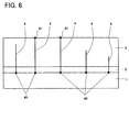
- FIG. 6 illustrates a schematic view showing a structure of a conventional group III nitride compound semiconductor.
- a buffer layer 2 and a group III nitride compound semiconductor layer 3 are formed successively on a substrate 1.
- the substrate 1 and the buffer layer 2 are made of sapphire and aluminum nitride (AlN), respectively.
- AlN buffer layer 2 is formed to relax misfit between the sapphire substrate 1 and the group III nitride compound semiconductor layer 3, possibility of generating dislocations cannot be 0.
- Feedthrough dislocations 4 are propagated from dislocation generating points 40 in longitudinal direction (a direction vertical to a surface of the substrate), penetrating the buffer layer 2 and the group III nitride compound semiconductor layer 3.
- manufacturing a semiconductor device by laminating various group III nitride compound semiconductor layers on the group III nitride compound semiconductor layer 3 results in propagating feedthrough dislocations 4 from dislocation generating points 41 which reach the surface of the group III nitride compound semiconductor layer 3, further through the semiconductor device in longitudinal direction. Accordingly, it had been difficult to prevent dislocations from propagating in the semiconductor device at the time when a group III nitride compound semiconductor layer is formed.
- an object of the present invention is to realize an efficient method capable of forming a layer of a group III nitride compound semiconductor without generation of cracks and dislocations to thereby improve device characteristics.
- the present invention has a first feature that resides in a method for manufacturing a group III nitride compound semiconductor, which hardly grows epitaxially on a substrate, by crystal growth, comprising: forming a buffer layer on a substrate into an island pattern such as a dot pattern, a striped pattern, or a grid pattern such that substrate-exposed portions are formed in a scattered manner; and forming a group III nitride compound semiconductor layer on the buffer layer by growing a group III nitride compound epitaxially in longitudinal and lateral directions.
- forming substrate-exposed portions in a scattered manner does not necessarily represent the condition that each substrate-exposed portions is completely separated, but represents the condition that the buffer layer exists around arbitrary substrate-exposed portions.
- the following method can be applied: forming the buffer layer on the entire surface of the substrate and then removing the desired portions of the buffer layer by etching; or forming a selective mask such as an SiO 2 film on the substrate and partially forming the buffer layer.
- the "lateral" direction as used in the specification refers to a direction parallel to a surface of the substrate.
- the group III nitride compound semiconductor grows on the buffer layer in a longitudinal direction.
- the group III nitride compound semiconductor which grows on the buffer layer in a longitudinal direction also grows in a lateral direction in order to cover the substrate-exposed portions.
- the growth velocity of the group III nitride compound semiconductor in the longitudinal and lateral directions can be controlled by conditions of, for example, temperature, pressure, or supplying conditions of source materials.
- a group III nitride compound semiconductor layer reunited into one layer can cover the substrate-exposed portions which are not covered by the buffer layer from a base of the buffer layer which is formed into an island pattern such as a dot pattern, a striped pattern or a grid pattern.
- feedthrough dislocations of the group III nitride compound semiconductor exists only in the regions of group III nitride compound semiconductor layer formed on the buffer layer, which is formed into an island pattern such as a dot pattern, a striped pattern or a grid pattern. This is because feedthrough dislocations are not generated when the group III nitride compound semiconductor grows in a lateral direction but are generated when it grows in a longitudinal direction.
- the second feature of the present invention is a method for manufacturing a group III nitride compound semiconductor, which hardly grows epitaxially on a substrate, by crystal growth, comprising: forming a buffer layer on a substrate into an island pattern such as a dot pattern, a striped pattern, or a grid pattern such that substrate-exposed portions are formed in a scattered manner; forming a group III nitride compound semiconductor layer on the buffer layer by growing a group III nitride compound epitaxially in longitudinal and lateral directions; etching at least one of the regions of the group III nitride compound semiconductor layer, growing in a longitudinal direction on the buffer layer which is formed into an island pattern; and growing the group III nitride compound semiconductor, which is left without being etched, in a lateral direction. Forming substrate-exposed portions in a scattered manner is explained in the first feature.
- the group III nitride compound semiconductor layer is etched after carrying out the method of the first feature, and then it is grown in a lateral direction in order to cover the etched regions.
- the surface density of longitudinal feedthrough dislocations of the group III nitride compound semiconductor layer decreases, and crystallinity of the device is thus improved.
- feedthrough dislocations generated by the longitudinal growth of the semiconductor layer can be eliminated. It is preferable to also etch the buffer layer to expose the substrate during etching of the group III nitride compound semiconductor layer.
- the substrate-exposed regions can be covered and a group III nitride compound semiconductor layer which is reunited into one layer can be obtained.
- the lateral growth can be promoted by the conditions of, for example, temperature, pressure, or supplying conditions of source materials.
- feedthrough dislocations existing in the group III nitride compound semiconductor layer can be eliminated.
- the group III nitride compound semiconductor layer does not have longitudinal feedthrough dislocations, and crystallinity of the device is, therefore, improved.
- the scope of the present invention also involves a method of etching regions of the group III nitride compound semiconductor layer, including the upper surface of the buffer layer, wider than the width of the buffer layer in case that feedthrough dislocations are generated partially inclined (in a lateral direction).
- all the regions of the group III nitride compound semiconductor layer which have feedthrough dislocations and grow on the buffer layer, which is formed into an island pattern such as a dot pattern, a striped pattern, or a grid pattern is not necessarily etched.
- the group III nitride compound semiconductor layer can be reunited into one layer by growing it in a lateral direction again, even when feedthrough dislocations are left without being etched in the semiconductor layer.
- the scope of the present invention also involves a method of dividing etching and epitaxial lateral overgrowth (ELO) components into several parts, according to a position or a design of the regions to form the buffer layer and limitations in the process afterward.
- ELO epitaxial lateral overgrowth
- the third feature of the present invention is to combine epitaxial growth of a group III nitride compound semiconductor layer formed on the buffer layer in longitudinal direction and epitaxial growth of the group III nitride compound in a lateral direction by using the difference between the velocities of epitaxial growth of the group III nitride compound semiconductor layer on the buffer layer and on the exposed substrate, in order to obtain a group III nitride compound semiconductor layer which covers the surface of the substrate.
- the difference between the velocities of epitaxial growth of the group III nitride compound semiconductor on the buffer layer and on the substrate can be easily controlled by the conditions of, for example, temperature, pressure, or supplying conditions of source materials.
- the velocities of growing the group III nitride compound semiconductor epitaxially on the buffer layer in longitudinal and lateral directions can be controlled. By controlling these conditions, surface density of feedthrough dislocations of the group III nitride compound semiconductor layer in longitudinal direction is decreased, and crystallinity of the device is improved.
- the difference between the velocities of epitaxial growth of the group III nitride compound semiconductor on the buffer layer and on the substrate is used.
- the group III nitride compound semiconductor comprises a compound which is identical to that of the buffer layer in view of stoichiometric composition.
- the compound of the group III nitride compound semiconductor can be non-crystalline, a set of micro-crystalline and polycrystalline, or single-crystalline.
- the difference between the velocities of epitaxial growth of the group III nitride compound semiconductor layer on the buffer layer and on the exposed substrate is an essential point of the present invention, and combination of the group III nitride compound, the compound forming the buffer layer, and materials to form the substrate is a method of generating the different epitaxial growth velocities.
- the fourth feature of the present invention is that the substrate is made of sapphire. As a result, it is difficult to epitaxially grow the group III nitride compound semiconductor on the substrate.
- the fifth feature of the present invention is that the buffer layer is made of aluminum nitride (AlN). And the sixth feature of the present invention is that the group III nitride compound semiconductor which grows in lateral direction does not comprise aluminum (Al).
- the seventh feature of the present invention is to obtain a light-emitting group III nitride compound semiconductor device by forming an another group III nitride compound semiconductor layer on the group III nitride compound semiconductor, which is formed on the region where the buffer layer is not formed, by using the above-described method. Because the group III nitride compound semiconductor layer is laminated on the regions which have no surface density of longitudinal feedthrough dislocations, reliability of the device is improved.
- the eighth feature of the present invention is to obtain only the group III nitride compound semiconductor layer by using the above-described method.
- the group III nitride compound semiconductor layer which is a layer laminated on the substrate, is left by removing the substrate. If necessary, the buffer layer can be removed with the substrate.
- the group III nitride compound semiconductor layer can dope an arbitrary dopant into the substrate so that the substrate has an arbitrary resistivity, and the group III nitride compound semiconductor layer with non-insulated substrate can be obtained. Because the group III nitride compound semiconductor layer has little or no surface density of feedthrough dislocations, it can be useful as a semiconductor substrate.
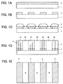
- FIGS. 1A-1E, 3A-3C, and 4A-4C each show views of processes for manufacturing a group III nitride compound semiconductor according to the first embodiment of the present invention.
- the group III nitride compound semiconductor of the present invention is formed through the use of a metal organic vapor phase epitaxy (hereinafter referred to as "MOVPE") method.
- Gases used in the MOVPE method are ammonia (NH 3 ), carrier gas (H 2 , or N 2 ), trimethyl gallium (Ga(CH 3 ) 3 ) (hereinafter referred to as "TMG”), and trimethyl aluminum (Al(CH 3 ) 3 ) (hereinafter referred to as "TMA").
- a single crystalline sapphire substrate 1 is formed to have a main surface 'a' which is cleaned by an organic washing solvent and heat treatment.
- An AlN buffer layer 2, having a thickness of about 40nm, is then formed on the surface 'a' of the sapphire substrate 1 under conditions controlled by lowering the temperature to 400°C and concurrently supplying H 2 , NH 3 and TMA at a flow rate of 10L/min, 5L/min, and 20 ⁇ mol/min, respectively, for 3 minutes (FIG. 1A).
- the buffer layer 2 is then dry-etched in a striped pattern by selective dry-etching including reactive ion etching (RIE) using a hard baked resist mask.
- RIE reactive ion etching
- the AlN buffer layer 2 is formed in a striped pattern such that each region defined above the buffer layer 2, has a width of 5 ⁇ m, and each region where the sapphire substrate 1 was exposed, has a width of 5 ⁇ m, and are formed alternately (FIGS. 1B and 1E).
- GaN layer 3 having a thickness of several thousands ⁇ was grown to cover the entire surface of the substrate and the AlN buffer layer, while maintaining the substrate 1 at a temperature of 1150°C, and feeding H 2 , NH 3 and TMG at 20L/min, 10L/min and 5 ⁇ mol/min, respectively. TMG is then fed at 300 ⁇ mol/min, thereby obtaining about 3 ⁇ m in thickness of GaN layer 3 at a growth temperature of 1000°C.
- the GaN layer 3 was formed by growing GaN regions 32 epitaxially on the sapphire substrate 1 in a lateral direction, from the GaN regions 31 which grows epitaxially on the upper surface of the AlN buffer layer 2 in a longitudinal direction and serves as a nucleus (FIGS. 1C and 1D). Accordingly, GaN regions 32 having excellent crystallinity can be obtained on the regions where the AlN buffer layer 2 is not formed and the sapphire substrate 1 is exposed.
- a group III nitride compound semiconductor device can be formed using the GaN regions 32 having excellent crystallinity, which is formed by epitaxial lateral overgrowth (ELO) method on the upper surface of the sapphire substrate 1, where predetermined regions of the substrate 1 for forming the device are exposed.
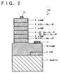
- FIG. 2 illustrates a device 100 comprising an LD formed on the GaN regions of high crystallinity in a Si-doped n-type GaN layer 30.
- the n-GaN regions of high crystallinity is formed in the regions where the AlN buffer layer is not formed, and the following layers are laminated in sequence on each of the regions: an n-Al 0.07 Ga 0.93 N cladding layer 4c; an n-GaN guide layer 5; an emission layer 6 having a multiple quantum well (MQW) structure, in which a well layer 61 made of Ga 0.9 In 0.1 N and a barrier layer 62 made of Ga 0.97 In 0.03 N were laminated alternately; a p-GaN guide layer 7; a p-Al 0.07 Ga 0.93 N cladding layer 8; and a p-GaN contact layer 9.
- MQW multiple quantum well
- electrodes 11 and 10 are formed on the n-GaN layer 30 and the p-GaN contact layer 9, respectively. Because the LD shown in FIG. 2 does not have feedthrough dislocations except around the electrode 11, reliability of the LD as a device is improved.
- a single crystalline sapphire substrate 1 is formed to have a main surface 'a' which is cleaned by an organic washing solvent and heat treatment.
- An AlN buffer layer 2, having a thickness of about 40nm is then formed on the surface 'a' of the sapphire substrate 1 under conditions controlled by lowering the temperature to 400°C and concurrently supplying H 2 , NH 3 and TMA at a flow rate of 10L/min, 5L/min, and 20 ⁇ mol/min, respectively, for 3 minutes.
- the buffer layer 2 is dry-etched in a striped pattern by selective dry-etching including reactive ion etching (RIE) using a hard baked resist mask.
- RIE reactive ion etching
- the AlN buffer layer 2 is formed in a striped pattern such that each region defined above the buffer layer 2, has a width of 5 ⁇ m, and each region where the sapphire substrate 1 is exposed, has a width of 5 ⁇ m, and are formed alternately.
- a GaN layer 3 having a thickness of several thousands ⁇ is grown to cover the entire surface of the substrate and the AlN buffer layer, while maintaining the substrate 1 at a temperature of 1150°C, and feeding H 2 , NH 3 and TMG were fed at 20L/min, 10L/min and 5 ⁇ mol/min, respectively. TMG is then fed at 300 ⁇ mol/min, thereby obtaining about 3 ⁇ m in thickness of GaN layer 3 at a growth temperature of 1000°C.
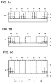
- the GaN layer 3 is formed by growing GaN regions 32 epitaxially on the sapphire substrate 1 in a lateral direction, from the GaN regions 31 which grow epitaxially on the upper surface of the AlN buffer layer 2 in a longitudinal direction and serves as a nucleus (FIG. 3A).
- the GaN regions 31 which grow epitaxially on the upper surface of the AlN buffer layer 2 in a longitudinal direction is dry-etched by selective etching (FIG. 3B).
- AlN buffer layer 2 is also etched.
- a film 3 having a thickness of several thousands ⁇ is formed to cover the entire surface of the group III nitride compound semiconductor, while maintaining the substrate 1 at a temperature of 1150°C, and feeding H 2 , NH 3 and TMG at 20L/min, 10L/min and 5 ⁇ mol/min, respectively. TMG is then fed at 300 ⁇ mol/min, thereby obtaining about 3 ⁇ m in thickness of GaN layer 3 at a growth temperature of 1000°C.
- GaN region 32 and GaN region 33 both have high crystallinity, and are formed on the sapphire substrate 1.
- the GaN region 32 is formed on the sapphire substrate 1 which is exposed by dry-etching the AlN buffer layer 2.
- the GaN region 33 is formed on the sapphire substrate 1 which is exposed by dry-etching the GaN regions 31 and the AlN buffer layer 2.
- a GaN layer 3 which has excellent crystallinity and does not have feedthrough dislocations, can be formed over a wide area W as shown in FIG. 3C.
- FIGS. 4A-4C are plan views of FIGS. 3A-3C.
- a GaN layer of excellent crystallinity is formed on a region other than a portion where the GaN region 31, which grows epitaxially on the upper surface of the AlN buffer layer 2 in a longitudinal direction, are formed.
- FIG. 4A illustrates the buffer layer 2 which is formed in a striped pattern. Regions represented by B are where the sapphire substrate 1 is exposed.
- FIG. 4B shows the GaN layer 3 left after etching the GaN region 31 and the buffer layer 2 thereunder, which grows epitaxially on the buffer layer 2 in a longitudinal direction. As shown in FIG. 4B, the GaN region 31 which has feedthrough dislocations is left at both sides of the substrate in order to support the GaN regions 32 of higher crystallinity, thus, preventing the GaN region 32 from peeling.
- FIG. 4C shows the GaN layer 3 reunited into one layer by epitaxial lateral overgrowth (ELO). As shown in FIG. 4C, the GaN layer 3 comprises GaN regions 31, 32 and 33.
- ELO epitaxial lateral overgrowth
- the GaN region 31 is formed on the buffer layer 2 and has feedthrough dislocations.
- the GaN region 32 is formed on the exposed substrate 1 and has no feedthrough dislocations.
- the GaN region 33 is formed after removing the buffer layer 2 and the GaN layer 31 and has no feedthrough dislocations. Accordingly, the crystallinity of GaN regions 32 and 33, or a region W, which has no feedthrough dislocations, is very desirable.
- the sapphire substrate 1 and the buffer layer 2 are removed by machinery polishing and then the GaN region 31 which has feedthrough dislocations and is at both side of the substrate is cut.
- the width of the regions defined above the AlN buffer layer 2, which are formed in a striped pattern is 5 ⁇ m
- a preferred range for the width is from 1 ⁇ m to 10 ⁇ m. This is because when the width of the regions becomes larger than 10 ⁇ m, the probability of generating dislocations increases. When the width of the regions becomes smaller than 1 ⁇ m, obtaining a GaN layer 3 with wide area and high quality becomes difficult.
- a width b of the regions B where the substrate 1 is exposed has a width of about 5 ⁇ m, a preferred range for the width is from 1 ⁇ m to 10 ⁇ m.
- a preferred range for thickness of the n-layer 3 made of GaN is 50 ⁇ m to 100 ⁇ m, because the n-layer 3 can be formed without dislocations.
- the buffer layer 2 and the group III nitride compound semiconductor layer 3 comprise aluminum nitride (AlN) and gallium nitride (GaN), respectively. Alternatively, these materials are not limited to AlN and GaN, respectively.
- An essential point of the present invention is to grow the group III nitride compound semiconductor, which does not grow epitaxially on the substrate, on the buffer layer epitaxially in a longitudinal direction and on the exposed substrate portion in a lateral direction, in order to form regions without feedthrough dislocations.
- the materials of the substrate, the buffer layer, and the composition ratio of the group III nitride compound semiconductor can be combined in different ways in accordance with different conditions for epitaxial growth.
- sapphire is used to form the substrate 1.
- silicon Si
- silicon carbide SiC
- other materials can be used.
- aluminum nitride is used to form the buffer layer 2.
- gallium nitride (GaN), gallium indium nitride (Ga x In 1-x N, 0 ⁇ x ⁇ 1), aluminum gallium nitride (Al x Ga 1-x N, 0 ⁇ x ⁇ 1) or aluminum gallium indium nitride (Al x Ga y In 1-x-y N, 0 ⁇ x ⁇ 1, 0 ⁇ y ⁇ 1, 0 ⁇ x+y ⁇ 1) may also be used.
- the buffer layer 2 is formed in a striped pattern.
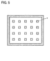
- the buffer layer 2 can be formed into an island pattern by exposing the substrate 1 in a grid pattern as shown in FIG. 5.
- the buffer layer 2 surrounds the peripheral surface of the substrate in FIG. 5, it is not necessarily present.
- a group III nitride compound semiconductor substrate can be obtained. Except when selectivity of epitaxial growth is prevented, an arbitrary dopant such as silicon (Si), germanium (Ge), zinc (Zn), indium (In), or magnesium (Mg) may be doped into the group III nitride compound semiconductor substrate. Accordingly, the group III nitride compound semiconductor substrate which has an arbitrary resistivity and includes an arbitrary dopant may be obtained.
- a light-emitting diode or a laser device comprising various group III nitride compound semiconductors, which is well known to have a double hetero structure comprising a guide layer, a cladding layer, an active layer having an MQW or SQW structure can be formed in the group III nitride compound semiconductor substrate of the present invention.
- a resonator facet can be easily cleaved because all the layers from the substrate to other layers are made of group III nitride compound semiconductors. As a result, oscillation efficiency of the laser can be improved.
- the group III nitride compound semiconductor substrate to have conductivity, electric current can flow in a vertical direction to the surface of the substrate.
- a process for forming an electrode can be simplified and the sectional area of the current path becomes wider and the length becomes shorter, resulting in lowering a driving voltage of the device.
- the MOVPE method is carried out under normal pressure.
- the MOVPE method can be carried out under reduced pressure. Further alternatively, it can be carried out under conditions combining normal pressure and reduced pressure.
- the group III nitride compound semiconductor of the present invention can be applied not only to a light-emitting device such as an LED or an LD but also to a light-receiving device or an electronic device.
- a buffer layer 2 made of aluminum nitride (AlN) is formed on a substrate 1 and is formed into an island pattern such as a dot pattern, a striped pattern, or a grid pattern such that substrate-exposed portions are formed in a scattered manner.
- a group III nitride compound semiconductor 3 grows epitaxially on the buffer layer 2 in a longitudinal direction, and grows epitaxially on the substrate-exposed portions in a lateral direction. As a result, a group III nitride compound semiconductor 3 which has little or no feedthrough dislocations 4 is obtained.
- region 32 Because the region where the group III nitride compound semiconductor 3 grows epitaxially in a lateral direction, on region 32, has excellent crystallinity, forming a group III nitride compound semiconductor device on the upper surface of the region results in improved device characteristics.
Landscapes
- Semiconductor Lasers (AREA)
- Led Devices (AREA)
- Crystals, And After-Treatments Of Crystals (AREA)
Applications Claiming Priority (2)
| Application Number | Priority Date | Filing Date | Title |
|---|---|---|---|
| JP12932299A JP3587081B2 (ja) | 1999-05-10 | 1999-05-10 | Iii族窒化物半導体の製造方法及びiii族窒化物半導体発光素子 |
| JP12932299 | 1999-05-10 |
Publications (1)
| Publication Number | Publication Date |
|---|---|
| EP1052684A1 true EP1052684A1 (de) | 2000-11-15 |
Family
ID=15006728
Family Applications (1)
| Application Number | Title | Priority Date | Filing Date |
|---|---|---|---|
| EP00109798A Withdrawn EP1052684A1 (de) | 1999-05-10 | 2000-05-09 | Verfahren zum Herstellen einer Nitridverbindung der Gruppe III und lichtemittierende Halbleitervorrichtung aus einer Nitridverbindung |
Country Status (3)
| Country | Link |
|---|---|
| US (2) | US6645295B1 (de) |
| EP (1) | EP1052684A1 (de) |
| JP (1) | JP3587081B2 (de) |
Cited By (14)
| Publication number | Priority date | Publication date | Assignee | Title |
|---|---|---|---|---|
| WO2002064864A1 (en) | 2001-02-14 | 2002-08-22 | Toyoda Gosei Co., Ltd. | Production method for semiconductor crystal and semiconductor luminous element |
| WO2002078069A1 (en) * | 2001-03-27 | 2002-10-03 | Sony Corporation | Nitride semiconductor element and production method thereof |
| WO2002071458A3 (en) * | 2001-02-28 | 2003-02-13 | Motorola Inc | Growth of compound semiconductor structures on patterned oxide films |
| WO2004023536A1 (en) * | 2002-09-03 | 2004-03-18 | University Of Warwick | Formation of lattice-tuning semiconductor substrates |
| WO2005106985A3 (en) * | 2004-04-22 | 2006-02-02 | Cree Inc | Improved substrate buffer structure for group iii nitride devices |
| EP1378949A4 (de) * | 2001-03-21 | 2006-03-22 | Mitsubishi Cable Ind Ltd | Lichtemittierendes halbleiterbauelement |
| EP1479795A4 (de) * | 2002-02-28 | 2006-12-20 | Toyoda Gosei Kk | Verfahren zur herstellung eines gruppe-iii-nitrid-verbindungshalbleiters |
| EP1245701A3 (de) * | 2001-03-28 | 2009-03-04 | Ngk Insulators, Ltd. | Verfahren zur Herstellungen eines Films aus einem Gruppe III - Nitrid |
| WO2010056443A1 (en) * | 2008-10-30 | 2010-05-20 | S.O.I.Tec Silicon On Insulator Technologies | Methods of forming layers of semiconductor material having reduced lattice strain, semiconductor structures, devices and engineered substrates including same |
| WO2012171736A1 (de) * | 2011-06-15 | 2012-12-20 | Osram Opto Semiconductors Gmbh | Optoelektronischer halbleiterkörper und verfahren zur herstellung eines optoelektronischen halbleiterkörpers |
| US8486771B2 (en) | 2008-09-24 | 2013-07-16 | Soitec | Methods of forming relaxed layers of semiconductor materials, semiconductor structures, devices and engineered substrates including same |
| US8637383B2 (en) | 2010-12-23 | 2014-01-28 | Soitec | Strain relaxation using metal materials and related structures |
| CN104221129A (zh) * | 2012-04-13 | 2014-12-17 | 坦德姆太阳能股份公司 | 基于外延生长来制造半导体设备的方法 |
| CN107130294A (zh) * | 2016-02-29 | 2017-09-05 | 信越化学工业株式会社 | 金刚石基板的制造方法,金刚石基板以及金刚石自立基板 |
Families Citing this family (60)
| Publication number | Priority date | Publication date | Assignee | Title |
|---|---|---|---|---|
| JP4817522B2 (ja) * | 2001-04-06 | 2011-11-16 | 三洋電機株式会社 | 窒化物系半導体層素子および窒化物系半導体の形成方法 |
| JP3956637B2 (ja) * | 2001-04-12 | 2007-08-08 | ソニー株式会社 | 窒化物半導体の結晶成長方法及び半導体素子の形成方法 |
| JP2003007999A (ja) * | 2001-06-26 | 2003-01-10 | Sony Corp | 窒化物系iii−v族化合物半導体基板およびその製造方法ならびに半導体発光素子の製造方法ならびに半導体装置の製造方法 |
| JP3864870B2 (ja) * | 2001-09-19 | 2007-01-10 | 住友電気工業株式会社 | 単結晶窒化ガリウム基板およびその成長方法並びにその製造方法 |
| WO2003089695A1 (en) | 2002-04-15 | 2003-10-30 | The Regents Of The University Of California | Non-polar a-plane gallium nitride thin films grown by metalorganic chemical vapor deposition |
| US8809867B2 (en) * | 2002-04-15 | 2014-08-19 | The Regents Of The University Of California | Dislocation reduction in non-polar III-nitride thin films |
| US7208393B2 (en) * | 2002-04-15 | 2007-04-24 | The Regents Of The University Of California | Growth of planar reduced dislocation density m-plane gallium nitride by hydride vapor phase epitaxy |
| JP2004107114A (ja) * | 2002-09-17 | 2004-04-08 | Toyoda Gosei Co Ltd | Iii族窒化物系化合物半導体基板の製造方法 |
| EP1576671A4 (de) * | 2002-12-16 | 2006-10-25 | Univ California | Wachstum von planarem, nichtpolarem a-ebenem galliumnitrid durch hydriddampffasenepitaxy |
| US7186302B2 (en) * | 2002-12-16 | 2007-03-06 | The Regents Of The University Of California | Fabrication of nonpolar indium gallium nitride thin films, heterostructures and devices by metalorganic chemical vapor deposition |
| US7427555B2 (en) * | 2002-12-16 | 2008-09-23 | The Regents Of The University Of California | Growth of planar, non-polar gallium nitride by hydride vapor phase epitaxy |
| US20060276043A1 (en) * | 2003-03-21 | 2006-12-07 | Johnson Mark A L | Method and systems for single- or multi-period edge definition lithography |
| US7504274B2 (en) * | 2004-05-10 | 2009-03-17 | The Regents Of The University Of California | Fabrication of nonpolar indium gallium nitride thin films, heterostructures and devices by metalorganic chemical vapor deposition |
| US7956360B2 (en) * | 2004-06-03 | 2011-06-07 | The Regents Of The University Of California | Growth of planar reduced dislocation density M-plane gallium nitride by hydride vapor phase epitaxy |
| US20080163814A1 (en) * | 2006-12-12 | 2008-07-10 | The Regents Of The University Of California | CRYSTAL GROWTH OF M-PLANE AND SEMIPOLAR PLANES OF (Al, In, Ga, B)N ON VARIOUS SUBSTRATES |
| KR100638609B1 (ko) | 2004-08-04 | 2006-10-26 | 삼성전기주식회사 | 질화물 반도체 결정성장방법 및 질화물 반도체 소자제조방법 |
| KR100918967B1 (ko) | 2004-12-29 | 2009-09-25 | 갤럭시아포토닉스 주식회사 | 버퍼층에 광 산란수단을 구비한 질화갈륨 소자 및 그제작방법 |
| US8324660B2 (en) | 2005-05-17 | 2012-12-04 | Taiwan Semiconductor Manufacturing Company, Ltd. | Lattice-mismatched semiconductor structures with reduced dislocation defect densities and related methods for device fabrication |
| US9153645B2 (en) | 2005-05-17 | 2015-10-06 | Taiwan Semiconductor Manufacturing Company, Ltd. | Lattice-mismatched semiconductor structures with reduced dislocation defect densities and related methods for device fabrication |
| TW200703463A (en) * | 2005-05-31 | 2007-01-16 | Univ California | Defect reduction of non-polar and semi-polar III-nitrides with sidewall lateral epitaxial overgrowth (SLEO) |
| JP5024722B2 (ja) * | 2005-06-06 | 2012-09-12 | 住友電気工業株式会社 | 窒化物半導体基板とその製造方法 |
| US7777250B2 (en) | 2006-03-24 | 2010-08-17 | Taiwan Semiconductor Manufacturing Company, Ltd. | Lattice-mismatched semiconductor structures and related methods for device fabrication |
| KR101305761B1 (ko) * | 2006-06-13 | 2013-09-06 | 엘지이노텍 주식회사 | 반도체 발광소자 |
| US8173551B2 (en) | 2006-09-07 | 2012-05-08 | Taiwan Semiconductor Manufacturing Co., Ltd. | Defect reduction using aspect ratio trapping |
| US7875958B2 (en) | 2006-09-27 | 2011-01-25 | Taiwan Semiconductor Manufacturing Company, Ltd. | Quantum tunneling devices and circuits with lattice-mismatched semiconductor structures |
| WO2008051503A2 (en) | 2006-10-19 | 2008-05-02 | Amberwave Systems Corporation | Light-emitter-based devices with lattice-mismatched semiconductor structures |
| US8193020B2 (en) | 2006-11-15 | 2012-06-05 | The Regents Of The University Of California | Method for heteroepitaxial growth of high-quality N-face GaN, InN, and AlN and their alloys by metal organic chemical vapor deposition |
| JP2010509177A (ja) * | 2006-11-15 | 2010-03-25 | ザ リージェンツ オブ ザ ユニバーシティ オブ カリフォルニア | 有機金属化学気相成長法による、高品質のN面GaN、InNおよびAlNならびにそれらの合金のヘテロエピタキシャル成長の方法 |
| WO2008124154A2 (en) | 2007-04-09 | 2008-10-16 | Amberwave Systems Corporation | Photovoltaics on silicon |
| US8304805B2 (en) | 2009-01-09 | 2012-11-06 | Taiwan Semiconductor Manufacturing Company, Ltd. | Semiconductor diodes fabricated by aspect ratio trapping with coalesced films |
| US8237151B2 (en) | 2009-01-09 | 2012-08-07 | Taiwan Semiconductor Manufacturing Company, Ltd. | Diode-based devices and methods for making the same |
| US7825328B2 (en) | 2007-04-09 | 2010-11-02 | Taiwan Semiconductor Manufacturing Company, Ltd. | Nitride-based multi-junction solar cell modules and methods for making the same |
| US8329541B2 (en) | 2007-06-15 | 2012-12-11 | Taiwan Semiconductor Manufacturing Company, Ltd. | InP-based transistor fabrication |
| TWI385820B (zh) * | 2007-08-24 | 2013-02-11 | Sino American Silicon Prod Inc | 半導體發光元件及其製造方法 |
| DE112008002387B4 (de) | 2007-09-07 | 2022-04-07 | Taiwan Semiconductor Manufacturing Co., Ltd. | Struktur einer Mehrfachübergangs-Solarzelle, Verfahren zur Bildung einer photonischenVorrichtung, Photovoltaische Mehrfachübergangs-Zelle und Photovoltaische Mehrfachübergangs-Zellenvorrichtung, |
| TWI344225B (en) * | 2007-10-05 | 2011-06-21 | Sino American Silicon Prod Inc | Semiconductor light-emitting device and method of fabricating the same |
| JP5085369B2 (ja) * | 2008-02-18 | 2012-11-28 | 日本オクラロ株式会社 | 窒化物半導体発光装置及びその製造方法 |
| US8183667B2 (en) | 2008-06-03 | 2012-05-22 | Taiwan Semiconductor Manufacturing Co., Ltd. | Epitaxial growth of crystalline material |
| US8274097B2 (en) | 2008-07-01 | 2012-09-25 | Taiwan Semiconductor Manufacturing Company, Ltd. | Reduction of edge effects from aspect ratio trapping |
| US8779445B2 (en) * | 2008-07-02 | 2014-07-15 | Taiwan Semiconductor Manufacturing Company, Ltd. | Stress-alleviation layer for LED structures |
| US8981427B2 (en) | 2008-07-15 | 2015-03-17 | Taiwan Semiconductor Manufacturing Company, Ltd. | Polishing of small composite semiconductor materials |
| JP2010040867A (ja) | 2008-08-06 | 2010-02-18 | Showa Denko Kk | Iii族窒化物半導体積層構造体およびその製造方法 |
| US20100072515A1 (en) | 2008-09-19 | 2010-03-25 | Amberwave Systems Corporation | Fabrication and structures of crystalline material |
| CN102160145B (zh) | 2008-09-19 | 2013-08-21 | 台湾积体电路制造股份有限公司 | 通过外延层过成长的元件形成 |
| US8253211B2 (en) | 2008-09-24 | 2012-08-28 | Taiwan Semiconductor Manufacturing Company, Ltd. | Semiconductor sensor structures with reduced dislocation defect densities |
| JP5705207B2 (ja) | 2009-04-02 | 2015-04-22 | 台湾積體電路製造股▲ふん▼有限公司Taiwan Semiconductor Manufacturing Company,Ltd. | 結晶物質の非極性面から形成される装置とその製作方法 |
| CN101877377B (zh) * | 2009-04-30 | 2011-12-14 | 比亚迪股份有限公司 | 一种分立发光二极管的外延片及其制造方法 |
| WO2010140564A1 (ja) * | 2009-06-01 | 2010-12-09 | 三菱化学株式会社 | 窒化物半導体結晶およびその製造方法 |
| US9048385B2 (en) | 2009-06-24 | 2015-06-02 | Nichia Corporation | Nitride semiconductor light emitting diode |
| US9818857B2 (en) | 2009-08-04 | 2017-11-14 | Gan Systems Inc. | Fault tolerant design for large area nitride semiconductor devices |
| US9029866B2 (en) | 2009-08-04 | 2015-05-12 | Gan Systems Inc. | Gallium nitride power devices using island topography |
| JP5985393B2 (ja) | 2009-08-04 | 2016-09-06 | ジーエーエヌ システムズ インコーポレイテッド | アイランドマトリックス化窒化ガリウムマイクロ波トランジスタおよびパワースイッチングトランジスタ |
| CN102893392B (zh) * | 2010-04-13 | 2015-08-05 | Gan系统公司 | 采用孤岛拓扑结构的高密度氮化镓器件 |
| CN101931039B (zh) * | 2010-08-23 | 2012-07-25 | 安徽三安光电有限公司 | 具有双层交错贯穿孔洞的氮化镓基发光二极管及其制作工艺 |
| JP5117596B2 (ja) * | 2011-05-16 | 2013-01-16 | 株式会社東芝 | 半導体発光素子、ウェーハ、および窒化物半導体結晶層の製造方法 |
| CN104716241B (zh) * | 2015-03-16 | 2018-10-16 | 映瑞光电科技(上海)有限公司 | 一种led结构及其制作方法 |
| US11823900B2 (en) | 2018-10-10 | 2023-11-21 | The Johns Hopkins University | Method for printing wide bandgap semiconductor materials |
| US11056338B2 (en) | 2018-10-10 | 2021-07-06 | The Johns Hopkins University | Method for printing wide bandgap semiconductor materials |
| CN115036366A (zh) * | 2021-03-05 | 2022-09-09 | 联华电子股份有限公司 | 半导体装置及其制作方法 |
| WO2025115743A1 (ja) * | 2023-11-30 | 2025-06-05 | 京セラ株式会社 | 半導体基板並びにその製造方法および製造装置、半導体デバイス |
Citations (2)
| Publication number | Priority date | Publication date | Assignee | Title |
|---|---|---|---|---|
| EP0551721A2 (de) * | 1991-12-18 | 1993-07-21 | Amano, Hiroshi | Halbleiteranordnung auf Basis von Gallium-Nitrid und Verfahren zur Herstellung |
| EP0951055A2 (de) * | 1998-04-17 | 1999-10-20 | Hewlett-Packard Company | In einem Graben lateral gewachsene Epitaxie-Schicht |
Family Cites Families (77)
| Publication number | Priority date | Publication date | Assignee | Title |
|---|---|---|---|---|
| JPS5143944B2 (de) | 1972-03-15 | 1976-11-25 | ||
| JPS51137393A (en) | 1975-05-22 | 1976-11-27 | Mitsubishi Electric Corp | Manufacturing method for semiconductor light emitting device |
| JPS5534646A (en) | 1978-08-30 | 1980-03-11 | Sumitomo Metal Ind Ltd | Heating method for furnace body in blowing-in of shaft furnace |
| JPS57115849A (en) | 1981-01-12 | 1982-07-19 | Fujitsu Ltd | Manufacture of substrate for semiconductor device |
| JPS5833882A (ja) | 1981-08-21 | 1983-02-28 | Mitsubishi Electric Corp | 発光ダイオ−ドの製造方法 |
| JPH01316459A (ja) | 1988-06-15 | 1989-12-21 | Murata Mfg Co Ltd | インラインスパッタリング装置およびその方法 |
| JP2768988B2 (ja) | 1989-08-17 | 1998-06-25 | 三菱電機株式会社 | 端面部分コーティング方法 |
| JPH06105797B2 (ja) | 1989-10-19 | 1994-12-21 | 昭和電工株式会社 | 半導体基板及びその製造方法 |
| JP2623464B2 (ja) | 1990-04-27 | 1997-06-25 | 豊田合成株式会社 | 窒化ガリウム系化合物半導体発光素子 |
| JPH0484418A (ja) | 1990-07-27 | 1992-03-17 | Nec Corp | 異種基板上への3―v族化合物半導体のヘテロエピタキシャル成長法 |
| JP2954743B2 (ja) | 1991-05-30 | 1999-09-27 | 京セラ株式会社 | 半導体発光装置の製造方法 |
| JPH05110206A (ja) | 1991-10-16 | 1993-04-30 | Kubota Corp | 半導体発光素子の製造方法及びその製造装置 |
| JP2751963B2 (ja) | 1992-06-10 | 1998-05-18 | 日亜化学工業株式会社 | 窒化インジウムガリウム半導体の成長方法 |
| JP3133182B2 (ja) | 1992-11-27 | 2001-02-05 | ヱスビー食品株式会社 | 飲料の渋味・苦味の改良方法 |
| JPH07249830A (ja) | 1994-03-10 | 1995-09-26 | Hitachi Ltd | 半導体発光素子の製造方法 |
| JPH07273367A (ja) | 1994-04-01 | 1995-10-20 | Mitsubishi Cable Ind Ltd | 半導体基板の製造方法および発光素子の製造方法 |
| JPH0864791A (ja) | 1994-08-23 | 1996-03-08 | Matsushita Electric Ind Co Ltd | エピタキシャル成長方法 |
| JP3326545B2 (ja) | 1994-09-30 | 2002-09-24 | ローム株式会社 | 半導体発光素子 |
| JPH08222812A (ja) | 1995-02-17 | 1996-08-30 | Matsushita Electric Ind Co Ltd | 窒化ガリウム系化合物半導体の結晶成長方法 |
| DE69622277T2 (de) | 1995-09-18 | 2003-03-27 | Hitachi, Ltd. | Halbleitermaterial, verfahren zur herstellung des halbleitermaterials und eine halbleitervorrichtung |
| JP3396356B2 (ja) | 1995-12-11 | 2003-04-14 | 三菱電機株式会社 | 半導体装置,及びその製造方法 |
| US5798536A (en) | 1996-01-25 | 1998-08-25 | Rohm Co., Ltd. | Light-emitting semiconductor device and method for manufacturing the same |
| JP3139445B2 (ja) | 1997-03-13 | 2001-02-26 | 日本電気株式会社 | GaN系半導体の成長方法およびGaN系半導体膜 |
| CA2258080C (en) | 1997-04-11 | 2007-06-05 | Nichia Chemical Industries, Ltd. | Nitride semiconductor growth method, nitride semiconductor substrate, and nitride semiconductor device |
| JPH11191657A (ja) | 1997-04-11 | 1999-07-13 | Nichia Chem Ind Ltd | 窒化物半導体の成長方法及び窒化物半導体素子 |
| DE19715572A1 (de) | 1997-04-15 | 1998-10-22 | Telefunken Microelectron | Verfahren zum Herstellen von epitaktischen Schichten eines Verbindungshalbleiters auf einkristallinem Silizium und daraus hergestellte Leuchtdiode |
| JPH10321954A (ja) | 1997-05-15 | 1998-12-04 | Fuji Electric Co Ltd | Iii 族窒化物半導体素子およびその製造方法 |
| JP3551751B2 (ja) | 1997-05-16 | 2004-08-11 | 日亜化学工業株式会社 | 窒化物半導体の成長方法 |
| WO1999001594A1 (en) | 1997-07-03 | 1999-01-14 | Cbl Technologies | Thermal mismatch compensation to produce free standing substrates by epitaxial deposition |
| JPH1119167A (ja) | 1997-07-04 | 1999-01-26 | Matsushita Electric Ind Co Ltd | 炭酸入浴剤供給装置 |
| JP3189877B2 (ja) | 1997-07-11 | 2001-07-16 | 日本電気株式会社 | 低転位窒化ガリウムの結晶成長方法 |
| JPH1143398A (ja) | 1997-07-22 | 1999-02-16 | Mitsubishi Cable Ind Ltd | GaN系結晶成長用基板およびその用途 |
| JP3930161B2 (ja) | 1997-08-29 | 2007-06-13 | 株式会社東芝 | 窒化物系半導体素子、発光素子及びその製造方法 |
| JPH11135770A (ja) | 1997-09-01 | 1999-05-21 | Sumitomo Chem Co Ltd | 3−5族化合物半導体とその製造方法および半導体素子 |
| JPH11145519A (ja) | 1997-09-02 | 1999-05-28 | Toshiba Corp | 半導体発光素子、半導体発光装置および画像表示装置 |
| JP3491538B2 (ja) | 1997-10-09 | 2004-01-26 | 日亜化学工業株式会社 | 窒化物半導体の成長方法及び窒化物半導体素子 |
| JPH11135832A (ja) | 1997-10-26 | 1999-05-21 | Toyoda Gosei Co Ltd | 窒化ガリウム系化合物半導体及びその製造方法 |
| JP3036495B2 (ja) | 1997-11-07 | 2000-04-24 | 豊田合成株式会社 | 窒化ガリウム系化合物半導体の製造方法 |
| JP3456413B2 (ja) | 1997-11-26 | 2003-10-14 | 日亜化学工業株式会社 | 窒化物半導体の成長方法及び窒化物半導体素子 |
| JP3620269B2 (ja) | 1998-02-27 | 2005-02-16 | 豊田合成株式会社 | GaN系半導体素子の製造方法 |
| US6051849A (en) | 1998-02-27 | 2000-04-18 | North Carolina State University | Gallium nitride semiconductor structures including a lateral gallium nitride layer that extends from an underlying gallium nitride layer |
| JP3839580B2 (ja) | 1998-03-09 | 2006-11-01 | 株式会社リコー | 半導体基板の製造方法 |
| JPH11274082A (ja) | 1998-03-24 | 1999-10-08 | Fuji Electric Co Ltd | Iii 族窒化物半導体およびその製造方法、およびiii 族窒化物半導体装置 |
| JP3436128B2 (ja) | 1998-04-28 | 2003-08-11 | 日亜化学工業株式会社 | 窒化物半導体の成長方法及び窒化物半導体素子 |
| JPH11330546A (ja) | 1998-05-12 | 1999-11-30 | Fuji Electric Co Ltd | Iii族窒化物半導体およびその製造方法 |
| JP4390090B2 (ja) | 1998-05-18 | 2009-12-24 | シャープ株式会社 | GaN系結晶膜の製造方法 |
| JP3460581B2 (ja) | 1998-05-28 | 2003-10-27 | 日亜化学工業株式会社 | 窒化物半導体の成長方法及び窒化物半導体素子 |
| US6606335B1 (en) | 1998-07-14 | 2003-08-12 | Fujitsu Limited | Semiconductor laser, semiconductor device, and their manufacture methods |
| US6319742B1 (en) | 1998-07-29 | 2001-11-20 | Sanyo Electric Co., Ltd. | Method of forming nitride based semiconductor layer |
| JP3316479B2 (ja) | 1998-07-29 | 2002-08-19 | 三洋電機株式会社 | 半導体素子、半導体発光素子および半導体素子の製造方法 |
| JP3987660B2 (ja) | 1998-07-31 | 2007-10-10 | シャープ株式会社 | 窒化物半導体構造とその製法および発光素子 |
| JP2000044121A (ja) | 1998-08-03 | 2000-02-15 | Murata Mach Ltd | 紡績機のスライバ案内クリール |
| JP3201475B2 (ja) | 1998-09-14 | 2001-08-20 | 松下電器産業株式会社 | 半導体装置およびその製造方法 |
| JP3592553B2 (ja) | 1998-10-15 | 2004-11-24 | 株式会社東芝 | 窒化ガリウム系半導体装置 |
| JP2000150959A (ja) | 1998-11-18 | 2000-05-30 | Hitachi Ltd | 窒化ガリウム系化合物半導体発光素子 |
| JP2000174393A (ja) | 1998-12-04 | 2000-06-23 | Fuji Electric Co Ltd | Iii族窒化物半導体およびその製造方法、およびiii族窒化物半導体装置 |
| JP4304750B2 (ja) | 1998-12-08 | 2009-07-29 | 日亜化学工業株式会社 | 窒化物半導体の成長方法及び窒化物半導体素子 |
| JP3659050B2 (ja) | 1998-12-21 | 2005-06-15 | 日亜化学工業株式会社 | 窒化物半導体の成長方法及び窒化物半導体素子 |
| JP2000261106A (ja) | 1999-01-07 | 2000-09-22 | Matsushita Electric Ind Co Ltd | 半導体発光素子、その製造方法及び光ディスク装置 |
| JP3770014B2 (ja) | 1999-02-09 | 2006-04-26 | 日亜化学工業株式会社 | 窒化物半導体素子 |
| JP3594826B2 (ja) | 1999-02-09 | 2004-12-02 | パイオニア株式会社 | 窒化物半導体発光素子及びその製造方法 |
| DE60043122D1 (de) | 1999-03-17 | 2009-11-19 | Mitsubishi Chem Corp | Halbleiterbasis ihre Herstellung und Halbleiterkristallhersetllungsmethode |
| JP4288743B2 (ja) | 1999-03-24 | 2009-07-01 | 日亜化学工業株式会社 | 窒化物半導体の成長方法 |
| JP4231189B2 (ja) | 1999-04-14 | 2009-02-25 | パナソニック株式会社 | Iii族窒化物系化合物半導体基板の製造方法 |
| TW464953B (en) | 1999-04-14 | 2001-11-21 | Matsushita Electronics Corp | Method of manufacturing III nitride base compound semiconductor substrate |
| JP3786544B2 (ja) | 1999-06-10 | 2006-06-14 | パイオニア株式会社 | 窒化物半導体素子の製造方法及びかかる方法により製造された素子 |
| GB9913687D0 (en) | 1999-06-11 | 1999-08-11 | Canon Kk | Image processing apparatus |
| JP2000357820A (ja) | 1999-06-15 | 2000-12-26 | Pioneer Electronic Corp | 窒化ガリウム系半導体発光素子及びその製造方法 |
| JP3791246B2 (ja) | 1999-06-15 | 2006-06-28 | 日亜化学工業株式会社 | 窒化物半導体の成長方法、及びそれを用いた窒化物半導体素子の製造方法、窒化物半導体レーザ素子の製造方法 |
| JP4005275B2 (ja) | 1999-08-19 | 2007-11-07 | 日亜化学工業株式会社 | 窒化物半導体素子 |
| JP4274504B2 (ja) | 1999-09-20 | 2009-06-10 | キヤノン株式会社 | 半導体薄膜構造体 |
| JP2001111174A (ja) | 1999-10-06 | 2001-04-20 | Fuji Photo Film Co Ltd | 半導体素子用基板およびその製造方法およびその半導体素子用基板を用いた半導体素子 |
| JP4055304B2 (ja) | 1999-10-12 | 2008-03-05 | 豊田合成株式会社 | 窒化ガリウム系化合物半導体の製造方法 |
| JP2001122693A (ja) | 1999-10-22 | 2001-05-08 | Nec Corp | 結晶成長用下地基板およびこれを用いた基板の製造方法 |
| JP3518455B2 (ja) | 1999-12-15 | 2004-04-12 | 日亜化学工業株式会社 | 窒化物半導体基板の作製方法 |
| US6355497B1 (en) | 2000-01-18 | 2002-03-12 | Xerox Corporation | Removable large area, low defect density films for led and laser diode growth |
| JP3988018B2 (ja) | 2001-01-18 | 2007-10-10 | ソニー株式会社 | 結晶膜、結晶基板および半導体装置 |
-
1999
- 1999-05-10 JP JP12932299A patent/JP3587081B2/ja not_active Expired - Lifetime
-
2000
- 2000-05-09 US US09/566,917 patent/US6645295B1/en not_active Expired - Lifetime
- 2000-05-09 EP EP00109798A patent/EP1052684A1/de not_active Withdrawn
-
2002
- 2002-07-02 US US10/187,943 patent/US6790279B2/en not_active Expired - Lifetime
Patent Citations (2)
| Publication number | Priority date | Publication date | Assignee | Title |
|---|---|---|---|---|
| EP0551721A2 (de) * | 1991-12-18 | 1993-07-21 | Amano, Hiroshi | Halbleiteranordnung auf Basis von Gallium-Nitrid und Verfahren zur Herstellung |
| EP0951055A2 (de) * | 1998-04-17 | 1999-10-20 | Hewlett-Packard Company | In einem Graben lateral gewachsene Epitaxie-Schicht |
Non-Patent Citations (2)
| Title |
|---|
| HIRAMATSU K ET AL: "Selective area growth and epitaxial lateral overgrowth of GaN by metalorganic vapor phase epitaxy and hydride vapor phase epitaxy", MATERIALS SCIENCE AND ENGINEERING B,CH,ELSEVIER SEQUOIA, LAUSANNE, vol. 59, no. 1-3, 6 May 1999 (1999-05-06), pages 104 - 111, XP004173214, ISSN: 0921-5107 * |
| ISAMU AKASAKI ET AL: "EFFECTS OF AIN BUFFER LAYER ON CRYSTALLOGRAPHIC STRUCTURE AND ON ELECTRICAL AND OPTICAL PROPERTIES OF GAN AND GA1-XALXN (0 X 0.4) FILMS GROWN ON SAPPHIRE SUBSTRATE BY MOVPE", JOURNAL OF CRYSTAL GROWTH,NL,NORTH-HOLLAND PUBLISHING CO. AMSTERDAM, vol. 98, no. 1/02, 1 November 1989 (1989-11-01), pages 209 - 219, XP000084936, ISSN: 0022-0248 * |
Cited By (31)
| Publication number | Priority date | Publication date | Assignee | Title |
|---|---|---|---|---|
| EP1367150A4 (de) * | 2001-02-14 | 2008-05-28 | Toyoda Gosei Kk | Verfahren zur herstellung von halbleiterkristall und halbleiter-leuchtelement |
| WO2002064864A1 (en) | 2001-02-14 | 2002-08-22 | Toyoda Gosei Co., Ltd. | Production method for semiconductor crystal and semiconductor luminous element |
| WO2002071458A3 (en) * | 2001-02-28 | 2003-02-13 | Motorola Inc | Growth of compound semiconductor structures on patterned oxide films |
| EP1378949A4 (de) * | 2001-03-21 | 2006-03-22 | Mitsubishi Cable Ind Ltd | Lichtemittierendes halbleiterbauelement |
| WO2002078069A1 (en) * | 2001-03-27 | 2002-10-03 | Sony Corporation | Nitride semiconductor element and production method thereof |
| US6921673B2 (en) | 2001-03-27 | 2005-07-26 | Sony Corporation | Nitride semiconductor device and method of manufacturing the same |
| EP1245701A3 (de) * | 2001-03-28 | 2009-03-04 | Ngk Insulators, Ltd. | Verfahren zur Herstellungen eines Films aus einem Gruppe III - Nitrid |
| EP1479795A4 (de) * | 2002-02-28 | 2006-12-20 | Toyoda Gosei Kk | Verfahren zur herstellung eines gruppe-iii-nitrid-verbindungshalbleiters |
| WO2004023536A1 (en) * | 2002-09-03 | 2004-03-18 | University Of Warwick | Formation of lattice-tuning semiconductor substrates |
| CN100364052C (zh) * | 2002-09-03 | 2008-01-23 | 阿德弗西斯有限公司 | 晶格调谐半导体衬底的形成 |
| US7179727B2 (en) | 2002-09-03 | 2007-02-20 | Advancesis Limited | Formation of lattice-tuning semiconductor substrates |
| WO2005106985A3 (en) * | 2004-04-22 | 2006-02-02 | Cree Inc | Improved substrate buffer structure for group iii nitride devices |
| US7872268B2 (en) | 2004-04-22 | 2011-01-18 | Cree, Inc. | Substrate buffer structure for group III nitride devices |
| US8486771B2 (en) | 2008-09-24 | 2013-07-16 | Soitec | Methods of forming relaxed layers of semiconductor materials, semiconductor structures, devices and engineered substrates including same |
| CN102203904A (zh) * | 2008-10-30 | 2011-09-28 | S.O.I.探测硅绝缘技术公司 | 形成具有减小的晶格应变的半导体材料层、半导体结构、装置的方法及包含具有减小的晶格应变的半导体材料层、半导体结构、装置的工程衬底 |
| US8836081B2 (en) | 2008-10-30 | 2014-09-16 | Soitec | Semiconductor structures, devices and engineered substrates including layers of semiconductor material having reduced lattice strain |
| US9368344B2 (en) | 2008-10-30 | 2016-06-14 | Soitec | Semiconductor structures, devices and engineered substrates including layers of semiconductor material having reduced lattice strain |
| WO2010056443A1 (en) * | 2008-10-30 | 2010-05-20 | S.O.I.Tec Silicon On Insulator Technologies | Methods of forming layers of semiconductor material having reduced lattice strain, semiconductor structures, devices and engineered substrates including same |
| CN102203904B (zh) * | 2008-10-30 | 2013-11-20 | S.O.I.探测硅绝缘技术公司 | 形成具有减小的晶格应变的半导体材料层、半导体结构、装置的方法及包含具有减小的晶格应变的半导体材料层、半导体结构、装置的工程衬底 |
| US8278193B2 (en) | 2008-10-30 | 2012-10-02 | Soitec | Methods of forming layers of semiconductor material having reduced lattice strain, semiconductor structures, devices and engineered substrates including same |
| US9312339B2 (en) | 2010-12-23 | 2016-04-12 | Soitec | Strain relaxation using metal materials and related structures |
| US8637383B2 (en) | 2010-12-23 | 2014-01-28 | Soitec | Strain relaxation using metal materials and related structures |
| WO2012171736A1 (de) * | 2011-06-15 | 2012-12-20 | Osram Opto Semiconductors Gmbh | Optoelektronischer halbleiterkörper und verfahren zur herstellung eines optoelektronischen halbleiterkörpers |
| US9478945B2 (en) | 2011-06-15 | 2016-10-25 | Osram Opto Semiconductors Gmbh | Optoelectronic semiconductor body and method for producing an optoelectronic semiconductor body |
| CN104221129A (zh) * | 2012-04-13 | 2014-12-17 | 坦德姆太阳能股份公司 | 基于外延生长来制造半导体设备的方法 |
| EP2837021A4 (de) * | 2012-04-13 | 2016-03-23 | Tandem Sun Ab | Verfahren und vorrichtung zur herstellung eines halbleiters auf basis eines epitaxialwachstums |
| CN107130294A (zh) * | 2016-02-29 | 2017-09-05 | 信越化学工业株式会社 | 金刚石基板的制造方法,金刚石基板以及金刚石自立基板 |
| EP3211657A3 (de) * | 2016-02-29 | 2017-11-15 | Shin-Etsu Chemical Co., Ltd. | Verfahren zur herstellung eines diamantsubstrats, diamantsubstrat und freistehendes diamantsubstrat |
| US10253426B2 (en) | 2016-02-29 | 2019-04-09 | Shin-Etsu Chemical Co., Ltd. | Method for manufacturing diamond substrate |
| CN107130294B (zh) * | 2016-02-29 | 2021-05-28 | 信越化学工业株式会社 | 金刚石基板的制造方法,金刚石基板以及金刚石自立基板 |
| US11066757B2 (en) | 2016-02-29 | 2021-07-20 | Shin-Etsu Chemical Co., Ltd. | Diamond substrate and freestanding diamond substrate |
Also Published As
| Publication number | Publication date |
|---|---|
| US6645295B1 (en) | 2003-11-11 |
| US20020179005A1 (en) | 2002-12-05 |
| JP3587081B2 (ja) | 2004-11-10 |
| US6790279B2 (en) | 2004-09-14 |
| JP2000323417A (ja) | 2000-11-24 |
Similar Documents
| Publication | Publication Date | Title |
|---|---|---|
| US6790279B2 (en) | Method for manufacturing group III nitride compound semiconductor and a light-emitting device using group III nitride compound semiconductor | |
| US6841410B2 (en) | Method for forming group-III nitride semiconductor layer and group-III nitride semiconductor device | |
| US6967122B2 (en) | Group III nitride compound semiconductor and method for manufacturing the same | |
| JP3036495B2 (ja) | 窒化ガリウム系化合物半導体の製造方法 | |
| JP4032538B2 (ja) | 半導体薄膜および半導体素子の製造方法 | |
| JP3518455B2 (ja) | 窒化物半導体基板の作製方法 | |
| US6734503B2 (en) | Nitride-based semiconductor element | |
| US8330144B2 (en) | Semi-polar nitride-based light emitting structure and method of forming same | |
| EP1263031A1 (de) | Methode zur herstellung gruppe iii nitrid verbindungshalbleiter und gruppe iii nitrid verbindungshalbleiteranordnung | |
| JP4055304B2 (ja) | 窒化ガリウム系化合物半導体の製造方法 | |
| KR20030070094A (ko) | 결정막, 결정기판 및 반도체장치 | |
| US20050260781A1 (en) | Method for manufacturing gallium nitride compound semiconductor | |
| WO2003072856A1 (en) | Process for producing group iii nitride compound semiconductor | |
| JP2001313259A (ja) | Iii族窒化物系化合物半導体基板の製造方法及び半導体素子 | |
| EP1376664A1 (de) | Verfahren zur herstellung eines halbleiters mit gruppe-iii-nitridzusammensetzung und halbleiterbauelement mit gruppe-iii-nitridzusammensetzung | |
| JP4406999B2 (ja) | Iii族窒化物系化合物半導体の製造方法及びiii族窒化物系化合物半導体素子 | |
| JP3934320B2 (ja) | GaN系半導体素子とその製造方法 | |
| JP4051892B2 (ja) | Iii族窒化物系化合物半導体の製造方法及びiii族窒化物系化合物半導体素子 | |
| JP4016566B2 (ja) | Iii族窒化物系化合物半導体の製造方法及びiii族窒化物系化合物半導体素子 | |
| US20070099320A1 (en) | Method for manufacturing gallium nitride compound semiconductor | |
| JP4042775B2 (ja) | 半導体薄膜および半導体素子の製造方法 | |
| JP2005094029A (ja) | GaN系半導体およびその製造方法 | |
| JP4255937B2 (ja) | 半導体素子 | |
| JP2003073196A (ja) | 窒化物半導体基板およびその製造方法 | |
| JP2001274519A (ja) | 半導体素子用基板およびその製造方法およびそれを用いた半導体素子 |
Legal Events
| Date | Code | Title | Description |
|---|---|---|---|
| PUAI | Public reference made under article 153(3) epc to a published international application that has entered the european phase |
Free format text: ORIGINAL CODE: 0009012 |
|
| 17P | Request for examination filed |
Effective date: 20000509 |
|
| AK | Designated contracting states |
Kind code of ref document: A1 Designated state(s): DE FR GB |
|
| AX | Request for extension of the european patent |
Free format text: AL;LT;LV;MK;RO;SI |
|
| AKX | Designation fees paid |
Free format text: DE FR GB |
|
| 17Q | First examination report despatched |
Effective date: 20070328 |
|
| STAA | Information on the status of an ep patent application or granted ep patent |
Free format text: STATUS: THE APPLICATION IS DEEMED TO BE WITHDRAWN |
|
| 18D | Application deemed to be withdrawn |
Effective date: 20091201 |