EP1235372A2 - Digitaler Zitterdämpfer zweiter Ordnung - Google Patents
Digitaler Zitterdämpfer zweiter Ordnung Download PDFInfo
- Publication number
- EP1235372A2 EP1235372A2 EP01308864A EP01308864A EP1235372A2 EP 1235372 A2 EP1235372 A2 EP 1235372A2 EP 01308864 A EP01308864 A EP 01308864A EP 01308864 A EP01308864 A EP 01308864A EP 1235372 A2 EP1235372 A2 EP 1235372A2
- Authority
- EP
- European Patent Office
- Prior art keywords
- output
- coupled
- phase
- integrator
- input
- Prior art date
- Legal status (The legal status is an assumption and is not a legal conclusion. Google has not performed a legal analysis and makes no representation as to the accuracy of the status listed.)
- Withdrawn
Links
Images

Classifications
-
- H—ELECTRICITY
- H03—ELECTRONIC CIRCUITRY
- H03L—AUTOMATIC CONTROL, STARTING, SYNCHRONISATION OR STABILISATION OF GENERATORS OF ELECTRONIC OSCILLATIONS OR PULSES
- H03L7/00—Automatic control of frequency or phase; Synchronisation
- H03L7/06—Automatic control of frequency or phase; Synchronisation using a reference signal applied to a frequency- or phase-locked loop
- H03L7/08—Details of the phase-locked loop
- H03L7/099—Details of the phase-locked loop concerning mainly the controlled oscillator of the loop
- H03L7/0991—Details of the phase-locked loop concerning mainly the controlled oscillator of the loop the oscillator being a digital oscillator, e.g. composed of a fixed oscillator followed by a variable frequency divider
- H03L7/0992—Details of the phase-locked loop concerning mainly the controlled oscillator of the loop the oscillator being a digital oscillator, e.g. composed of a fixed oscillator followed by a variable frequency divider comprising a counter or a frequency divider
-
- H—ELECTRICITY
- H03—ELECTRONIC CIRCUITRY
- H03L—AUTOMATIC CONTROL, STARTING, SYNCHRONISATION OR STABILISATION OF GENERATORS OF ELECTRONIC OSCILLATIONS OR PULSES
- H03L7/00—Automatic control of frequency or phase; Synchronisation
- H03L7/06—Automatic control of frequency or phase; Synchronisation using a reference signal applied to a frequency- or phase-locked loop
- H03L7/08—Details of the phase-locked loop
- H03L7/081—Details of the phase-locked loop provided with an additional controlled phase shifter
- H03L7/0812—Details of the phase-locked loop provided with an additional controlled phase shifter and where no voltage or current controlled oscillator is used
- H03L7/0814—Details of the phase-locked loop provided with an additional controlled phase shifter and where no voltage or current controlled oscillator is used the phase shifting device being digitally controlled
-
- H—ELECTRICITY
- H03—ELECTRONIC CIRCUITRY
- H03L—AUTOMATIC CONTROL, STARTING, SYNCHRONISATION OR STABILISATION OF GENERATORS OF ELECTRONIC OSCILLATIONS OR PULSES
- H03L7/00—Automatic control of frequency or phase; Synchronisation
- H03L7/06—Automatic control of frequency or phase; Synchronisation using a reference signal applied to a frequency- or phase-locked loop
- H03L7/08—Details of the phase-locked loop
- H03L7/085—Details of the phase-locked loop concerning mainly the frequency- or phase-detection arrangement including the filtering or amplification of its output signal
- H03L7/093—Details of the phase-locked loop concerning mainly the frequency- or phase-detection arrangement including the filtering or amplification of its output signal using special filtering or amplification characteristics in the loop
Definitions
- the present invention relates to jitter attenuators.
- Jitter attenuators are used to compensate for phase variations in an input signal. Uncompensated jitter can be a significant source of error.
- transmission systems such as T3 and E3
- the clock is encoded with the data.
- a receiver will extract the clock from the coded datastream and provide the extracted clock and data itself. This clock can then be used to retransmit the data to the next node. Jitter is obviously undesirable since any phase variation of the clock can be passed along from node to node.
- the transmission media may transmit higher frequency portions of the signal faster than lower frequency portions.
- the received clock is filtered and smoothed to remove the jitter.
- An elastic buffer such as a FIFO, is sometimes used to buffer the difference in rates of the received jittery clock and the retransmitted data. See, for example, U.S. Patent No. 5,090,025.
- U.S. Patent No, 5,493,243 shows using an up/down counter and a subsequent decoder to control the digital frequency synthesizer.
- the input clock is used to decrement the counter, while the output, divided-down clock is used to increment the counter.
- Each change in the count causes a change in the phase of the synthesized frequency.
- the present invention provides a phase detector which detects the phase difference between the input clock and an output clock, That phase difference is used to gate a high frequency clock, which is provided to an integration circuit.
- the phase detector also indicates whether the phase difference is positive or negative.
- the output of the integration circuit is provided to a comparator, which compares the value to a threshold. When the threshold is exceeded, an advance or retard signal is provided to a phase selector, The phase selector selects one of multiple phases of a clock used for the output clock.
- the integration circuit has first and second integrators.
- the phase detector output is provided to the first integrator,
- the output of the first integrator is provided to an adder,
- the other input of the adder is the output of the phase detector scaled through a first scaling circuit.
- a second scaling factor is applied to the phase detector output.
- the adder output is then provided through a second integrator, with the output of the second integrator being provided to the comparator. This integration will result in minimizing any frequency offset.
- jitter is self-offsetting, or corrects it on the next or a close pulse
- the present invention will not change the output phase. For example, a positive integrated value may be offset by a subsequent negative integrated value. It is only when the total integrated value reaches a preselected threshold (positive or negative) that the output clock phase is adjusted. This ensures that the phase jitter is not transient. However, the threshold is selected low enough so that true jitter is compensated for sufficiently quickly.
- the invention uses a multiple phase clock generator operating off of a high frequency clock.
- One of the clock phases generated is selected by a phase selector connected to the output of the comparator.
- the selected clock is then divided down to the frequency of the input clock.
- the same high frequency clock used to generate the multiple phases is also used for the input phase detector.
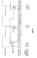
- Fig. 1 is a block diagram of an embodiment of the present invention.
- Fig. 2 is a timing diagram illustrating the operation of the embodiment of Fig. 1.
- Fig. 3 is a diagram of one embodiment of the phase detector of Fig. 1.
- Fig. 1 shows a jitter attenuator circuit 10 according to an embodiment of the invention.
- An input is provided through a divider 15(divide by 32) on a line 12 to a phase detector 14,
- the input is a T3/E3 clock recovered from a received signal.
- the input could alternately be another communication signal,
- the present invention could be used in a transceiver, such as a T3/E3 transceiver.
- a second input to phase detector 14 on line 17 is an output clock signal after jitter correction, provided through a divider 19 (divide by 32) to input line 16. This is fed back from the output of the circuit of Fig. 1.
- a high frequency clock signal is provided on a line 18.
- the high frequency clock is preferably selected to have a frequency which is a multiple of the input frequency used.
- the phase detector provides an output on a line 20 to the integration circuitry including integrators #1 and #2.
- the output on line 20 is provided to a first scaling factor circuit 21, and then to an adder 25. It is also provided through a second scaling factor circuit 23 to a first integrator 29.
- the output of integrator 29 is added back in adding circuit 25, with the output then being provided to a second integrator 27.
- FIG. 2 An example of the operation is illustrated by the signals in Fig. 2.
- the signals shown are the output clock 16 and input clock 12. Also shown is the high frequency clock 18.
- the phase detector detects the difference between the rising edges of the clocks on lines 12 and 16. This difference is indicated by arrows 26. This performs a gating of the high frequency clock 18, allowing three pulses in the example shown to be gated through to output line 20 and integrated,
- a subsequent difference in rising edges is shown by arrows 28, Here, the difference is negative, since the rising edge of the clock on the input line 12 is ahead of the output clock on line 16. As shown, two clock pulses of the high frequency clock are gated through. A negative value is applied to the integrators,
- phase difference continues to be negative, by an amount of 3. If this continues, this shows a jitter which is not transient.
- a retard signal can be provided on an output line to phase selector 34 as shown in Fig. 1. This will cause the phase selector to select a phase of the output clock which is retarded from that shown as output 16 in Fig. 2. This should close the phase difference gap.
- the double integration provides a measure of the cumulative value of the phase difference.
- a change in phase can be caused either by a large difference for a short time, or a small difference which persists for a long time.
- the circuit can control, through the scaling factors, the amount of the phase difference which is integrated.
- the portion which is integrated through scale factor circuit 21 is in effect subject to only a single integration.
- Integrator #2 provides a first order integration which reduces jitter. Integrator #1 provides compensation for frequency offsets, which require longer term correlation and an essentially constant offset.
- the phase selector 34 selects one of multiple phases of a clock signal from a multiple phase clock signal generator 36, As shown, M outputs of clock generator 36 are provided to phase selector 34, In one embodiment of the invention, M is 5.
- Clock generator 36 receives its input from the same high frequency clock line 18 that is provided to phase detector 14, The high frequency clock in one embodiment is 8 times the frequency of the input clock.
- phase selector 34 If the phase difference were to be positive, an advance signal would be output from comparator 31 on a line 38 to phase selector 34.
- the output of phase selector 34 is provided to a divide by N frequency divider 40, which divides the high frequency clock down to the same frequency as the input clock.
- An advantage of the invention is that the circuit can be designed and analyzed in the Z domain using a DSP (Digital Signal Processing) approach.
- the jitter transfer function is: ( a 1+ a 2) z - a 1 z 2 - z (2- a 1- a 2)+1- a 1
- phase selector 34 can be a multiplexer for multiplexing the various M phases of the clock, with logic selection circuitry controlled by the advance and retard signals on lines 32 and 38. In one embodiment, each advance or retard signal selects the next phase clock.
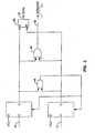
- Fig. 3 is one embodiment of a phase detector circuit.
- a pair of flip-flops 40 and 42 are used, with outputs connected to AND gate 44 and OR gate 46.
- the sign of the output is provided through latch 48 on line 50, while line 52 provides a window which gates the pulses from the high frequency clock on line 18.
- the scaling factor for scaling circuit 21 is 2 -12 and the scaling factor for scaling factor 23 is 2 -29 .
- the smaller scaling factor is used for the integrator #1 input so that the circuit will not change quickly.
- a larger frequency offset must be tolerated compared to a T1/E1 environment (relative to jitter cutoff frequency).
- the comparator can simply be the most significant bit (MSB) and the sign bit, which can be used to trigger the retard or advance. No actual comparison circuit is necessary in this embodiment,
- the integrator can be implemented as an adder. Integrator #1 can be thought of as storing information for the frequency offset.
- the frequency offset is compensated by a constant phase offset. This limits the allowable frequency offset of the incoming signal.
- a second order jitter attenuator uses a second integrator to store the frequency offset information. The phase offset can therefore be substantially eliminated,
- phase selector could select the multiple phases of a clock signal after they have been frequency-divided, rather than before.
- the specific scaling factors could be varied depending upon the application.
- one or more phases could be skipped, such as where the count is reached very quickly, indicating a larger correction is required. Accordingly, the foregoing description is intended to be illustrative, but not limiting, of the scope of the invention which is set forth in the following claims.
Landscapes
- Stabilization Of Oscillater, Synchronisation, Frequency Synthesizers (AREA)
- Synchronisation In Digital Transmission Systems (AREA)
Applications Claiming Priority (2)
| Application Number | Priority Date | Filing Date | Title |
|---|---|---|---|
| US728303 | 1985-04-29 | ||
| US09/728,303 US6333651B1 (en) | 2000-12-01 | 2000-12-01 | Second order digital jitter attenuator |
Publications (2)
| Publication Number | Publication Date |
|---|---|
| EP1235372A2 true EP1235372A2 (de) | 2002-08-28 |
| EP1235372A3 EP1235372A3 (de) | 2004-10-13 |
Family
ID=24926290
Family Applications (1)
| Application Number | Title | Priority Date | Filing Date |
|---|---|---|---|
| EP01308864A Withdrawn EP1235372A3 (de) | 2000-12-01 | 2001-10-18 | Digitaler Zitterdämpfer zweiter Ordnung |
Country Status (2)
| Country | Link |
|---|---|
| US (1) | US6333651B1 (de) |
| EP (1) | EP1235372A3 (de) |
Families Citing this family (3)
| Publication number | Priority date | Publication date | Assignee | Title |
|---|---|---|---|---|
| US7346701B2 (en) * | 2002-08-30 | 2008-03-18 | Broadcom Corporation | System and method for TCP offload |
| CN100508396C (zh) * | 2003-07-10 | 2009-07-01 | 瑞昱半导体股份有限公司 | 产生输出信号的方法及装置和锁相回路环 |
| CN1697324B (zh) * | 2004-05-10 | 2010-04-07 | 华为技术有限公司 | 传输信号去抖动的实现方法及其装置 |
Family Cites Families (8)
| Publication number | Priority date | Publication date | Assignee | Title |
|---|---|---|---|---|
| US4563657A (en) * | 1982-03-15 | 1986-01-07 | Codex Corporation | Frequency synthesizer and digital phase lock loop |
| US5056054A (en) * | 1990-05-02 | 1991-10-08 | National Semiconductor Corporation | Digital phase locked loop utilizing a multi-bit phase error input for control of a stepped clock generator |
| US5644605A (en) * | 1990-11-13 | 1997-07-01 | Dallas Semiconductor Corp. | Jitter attenuator |
| US5239561A (en) * | 1991-07-15 | 1993-08-24 | National Semiconductor Corporation | Phase error processor |
| US5493243A (en) * | 1994-01-04 | 1996-02-20 | Level One Communications, Inc. | Digitally controlled first order jitter attentuator using a digital frequency synthesizer |
| US5793824A (en) * | 1996-04-30 | 1998-08-11 | Adtran, Inc. | Digital phase locked loop having adaptive bandwidth for pulse stuffing synchronized digital communication system |
| US5966416A (en) * | 1996-11-21 | 1999-10-12 | Dsp Group, Inc. | Verification of PN synchronization in a spread-spectrum communications receiver |
| US6121816A (en) * | 1999-04-23 | 2000-09-19 | Semtech Corporation | Slave clock generation system and method for synchronous telecommunications networks |
-
2000
- 2000-12-01 US US09/728,303 patent/US6333651B1/en not_active Expired - Fee Related
-
2001
- 2001-10-18 EP EP01308864A patent/EP1235372A3/de not_active Withdrawn
Also Published As
| Publication number | Publication date |
|---|---|
| EP1235372A3 (de) | 2004-10-13 |
| US6333651B1 (en) | 2001-12-25 |
Similar Documents
| Publication | Publication Date | Title |
|---|---|---|
| US6351165B1 (en) | Digital jitter attenuator using an accumulated count of phase differences | |
| US5546432A (en) | Method and apparatus for attenuating jitter in a digital transmission line | |
| US7668271B2 (en) | Clock-data recovery (“CDR”) circuit, apparatus and method for variable frequency data | |
| KR100804286B1 (ko) | 다중-클럭 시스템에서 스킵 패턴을 동기화하고 클럭포워딩 인터페이스를 초기화하는 시스템 및 방법 | |
| US5694068A (en) | Digital phase-locked loop (PLL) having multilevel phase comparators | |
| EP2153523B1 (de) | Frequenzsynchronisation | |
| US20020196886A1 (en) | SYNC pulse compensation and regeneration in a clock synchronizer controller | |
| JPH0744449B2 (ja) | デイジタル・フエ−ズロツクル−プ回路 | |
| US8295423B2 (en) | System and method for clockless data recovery | |
| US4841548A (en) | Method and apparatus for extracting an auxiliary data clock from the clock and/or the clock-phase of a synchronous or plesiochronic digital signal | |
| US6333651B1 (en) | Second order digital jitter attenuator | |
| US7826581B1 (en) | Linearized digital phase-locked loop method for maintaining end of packet time linearity | |
| US8513994B2 (en) | State machine for deskew delay locked loop | |
| US4628519A (en) | Digital phase-locked loop circuit | |
| US7366207B1 (en) | High speed elastic buffer with clock jitter tolerant design | |
| US5396522A (en) | Method and apparatus for clock synchronization with information received by a radio receiver | |
| CN1615602B (zh) | 帧边界辨别器 | |
| JP3159585B2 (ja) | クロック抽出回路 | |
| JP2748875B2 (ja) | クロック抽出回路 | |
| SU1707620A1 (ru) | Устройство дл восстановлени информации | |
| JPH1188152A (ja) | ディジタルpll回路 | |
| JPH04357730A (ja) | シリアル伝送の同期化装置 | |
| JPH0983354A (ja) | Dpll回路 | |
| JPH0295015A (ja) | デジタルpll回路 | |
| JPS5936468B2 (ja) | 同期回路 |
Legal Events
| Date | Code | Title | Description |
|---|---|---|---|
| PUAI | Public reference made under article 153(3) epc to a published international application that has entered the european phase |
Free format text: ORIGINAL CODE: 0009012 |
|
| AK | Designated contracting states |
Kind code of ref document: A2 Designated state(s): AT BE CH CY DE DK ES FI FR GB GR IE IT LI LU MC NL PT SE TR |
|
| AX | Request for extension of the european patent |
Free format text: AL;LT;LV;MK;RO;SI |
|
| PUAL | Search report despatched |
Free format text: ORIGINAL CODE: 0009013 |
|
| AK | Designated contracting states |
Kind code of ref document: A3 Designated state(s): AT BE CH CY DE DK ES FI FR GB GR IE IT LI LU MC NL PT SE TR |
|
| AX | Request for extension of the european patent |
Extension state: AL LT LV MK RO SI |
|
| 17P | Request for examination filed |
Effective date: 20050323 |
|
| AKX | Designation fees paid |
Designated state(s): DE FR GB IT |
|
| 17Q | First examination report despatched |
Effective date: 20070315 |
|
| STAA | Information on the status of an ep patent application or granted ep patent |
Free format text: STATUS: THE APPLICATION IS DEEMED TO BE WITHDRAWN |
|
| 18D | Application deemed to be withdrawn |
Effective date: 20140503 |