EP1411547A2 - Film zum Schneiden und Zerteilen und Verfahren zur Befestigung von Halbleiterchips sowie Halbleiteranordnung - Google Patents
Film zum Schneiden und Zerteilen und Verfahren zur Befestigung von Halbleiterchips sowie Halbleiteranordnung Download PDFInfo
- Publication number
- EP1411547A2 EP1411547A2 EP03023536A EP03023536A EP1411547A2 EP 1411547 A2 EP1411547 A2 EP 1411547A2 EP 03023536 A EP03023536 A EP 03023536A EP 03023536 A EP03023536 A EP 03023536A EP 1411547 A2 EP1411547 A2 EP 1411547A2
- Authority
- EP
- European Patent Office
- Prior art keywords
- adhesive layer
- pressure
- die
- sensitive adhesive
- dicing
- Prior art date
- Legal status (The legal status is an assumption and is not a legal conclusion. Google has not performed a legal analysis and makes no representation as to the accuracy of the status listed.)
- Withdrawn
Links
Images


Classifications
-
- C—CHEMISTRY; METALLURGY
- C09—DYES; PAINTS; POLISHES; NATURAL RESINS; ADHESIVES; COMPOSITIONS NOT OTHERWISE PROVIDED FOR; APPLICATIONS OF MATERIALS NOT OTHERWISE PROVIDED FOR
- C09J—ADHESIVES; NON-MECHANICAL ASPECTS OF ADHESIVE PROCESSES IN GENERAL; ADHESIVE PROCESSES NOT PROVIDED FOR ELSEWHERE; USE OF MATERIALS AS ADHESIVES
- C09J7/00—Adhesives in the form of films or foils
- C09J7/20—Adhesives in the form of films or foils characterised by their carriers
-
- H—ELECTRICITY
- H10—SEMICONDUCTOR DEVICES; ELECTRIC SOLID-STATE DEVICES NOT OTHERWISE PROVIDED FOR
- H10P—GENERIC PROCESSES OR APPARATUS FOR THE MANUFACTURE OR TREATMENT OF DEVICES COVERED BY CLASS H10
- H10P54/00—Cutting or separating of wafers, substrates or parts of devices
-
- H—ELECTRICITY
- H10—SEMICONDUCTOR DEVICES; ELECTRIC SOLID-STATE DEVICES NOT OTHERWISE PROVIDED FOR
- H10P—GENERIC PROCESSES OR APPARATUS FOR THE MANUFACTURE OR TREATMENT OF DEVICES COVERED BY CLASS H10
- H10P72/00—Handling or holding of wafers, substrates or devices during manufacture or treatment thereof
- H10P72/70—Handling or holding of wafers, substrates or devices during manufacture or treatment thereof for supporting or gripping
- H10P72/74—Handling or holding of wafers, substrates or devices during manufacture or treatment thereof for supporting or gripping using temporarily an auxiliary support
- H10P72/7402—Wafer tapes, e.g. grinding or dicing support tapes
-
- H—ELECTRICITY
- H10—SEMICONDUCTOR DEVICES; ELECTRIC SOLID-STATE DEVICES NOT OTHERWISE PROVIDED FOR
- H10P—GENERIC PROCESSES OR APPARATUS FOR THE MANUFACTURE OR TREATMENT OF DEVICES COVERED BY CLASS H10
- H10P72/00—Handling or holding of wafers, substrates or devices during manufacture or treatment thereof
- H10P72/70—Handling or holding of wafers, substrates or devices during manufacture or treatment thereof for supporting or gripping
- H10P72/74—Handling or holding of wafers, substrates or devices during manufacture or treatment thereof for supporting or gripping using temporarily an auxiliary support
- H10P72/7402—Wafer tapes, e.g. grinding or dicing support tapes
- H10P72/7404—Wafer tapes, e.g. grinding or dicing support tapes the wafer tape being a laminate of three or more layers, e.g. including additional layers beyond a base layer and an uppermost adhesive layer
-
- C—CHEMISTRY; METALLURGY
- C09—DYES; PAINTS; POLISHES; NATURAL RESINS; ADHESIVES; COMPOSITIONS NOT OTHERWISE PROVIDED FOR; APPLICATIONS OF MATERIALS NOT OTHERWISE PROVIDED FOR
- C09J—ADHESIVES; NON-MECHANICAL ASPECTS OF ADHESIVE PROCESSES IN GENERAL; ADHESIVE PROCESSES NOT PROVIDED FOR ELSEWHERE; USE OF MATERIALS AS ADHESIVES
- C09J2203/00—Applications of adhesives in processes or use of adhesives in the form of films or foils
- C09J2203/326—Applications of adhesives in processes or use of adhesives in the form of films or foils for bonding electronic components such as wafers, chips or semiconductors
-
- C—CHEMISTRY; METALLURGY
- C09—DYES; PAINTS; POLISHES; NATURAL RESINS; ADHESIVES; COMPOSITIONS NOT OTHERWISE PROVIDED FOR; APPLICATIONS OF MATERIALS NOT OTHERWISE PROVIDED FOR
- C09J—ADHESIVES; NON-MECHANICAL ASPECTS OF ADHESIVE PROCESSES IN GENERAL; ADHESIVE PROCESSES NOT PROVIDED FOR ELSEWHERE; USE OF MATERIALS AS ADHESIVES
- C09J2301/00—Additional features of adhesives in the form of films or foils
- C09J2301/20—Additional features of adhesives in the form of films or foils characterized by the structural features of the adhesive itself
- C09J2301/208—Additional features of adhesives in the form of films or foils characterized by the structural features of the adhesive itself the adhesive layer being constituted by at least two or more adjacent or superposed adhesive layers, e.g. multilayer adhesive
-
- C—CHEMISTRY; METALLURGY
- C09—DYES; PAINTS; POLISHES; NATURAL RESINS; ADHESIVES; COMPOSITIONS NOT OTHERWISE PROVIDED FOR; APPLICATIONS OF MATERIALS NOT OTHERWISE PROVIDED FOR
- C09J—ADHESIVES; NON-MECHANICAL ASPECTS OF ADHESIVE PROCESSES IN GENERAL; ADHESIVE PROCESSES NOT PROVIDED FOR ELSEWHERE; USE OF MATERIALS AS ADHESIVES
- C09J2301/00—Additional features of adhesives in the form of films or foils
- C09J2301/30—Additional features of adhesives in the form of films or foils characterized by the chemical, physicochemical or physical properties of the adhesive or the carrier
- C09J2301/302—Additional features of adhesives in the form of films or foils characterized by the chemical, physicochemical or physical properties of the adhesive or the carrier the adhesive being pressure-sensitive, i.e. tacky at temperatures inferior to 30°C
-
- C—CHEMISTRY; METALLURGY
- C09—DYES; PAINTS; POLISHES; NATURAL RESINS; ADHESIVES; COMPOSITIONS NOT OTHERWISE PROVIDED FOR; APPLICATIONS OF MATERIALS NOT OTHERWISE PROVIDED FOR
- C09J—ADHESIVES; NON-MECHANICAL ASPECTS OF ADHESIVE PROCESSES IN GENERAL; ADHESIVE PROCESSES NOT PROVIDED FOR ELSEWHERE; USE OF MATERIALS AS ADHESIVES
- C09J2301/00—Additional features of adhesives in the form of films or foils
- C09J2301/30—Additional features of adhesives in the form of films or foils characterized by the chemical, physicochemical or physical properties of the adhesive or the carrier
- C09J2301/304—Additional features of adhesives in the form of films or foils characterized by the chemical, physicochemical or physical properties of the adhesive or the carrier the adhesive being heat-activatable, i.e. not tacky at temperatures inferior to 30°C
-
- C—CHEMISTRY; METALLURGY
- C09—DYES; PAINTS; POLISHES; NATURAL RESINS; ADHESIVES; COMPOSITIONS NOT OTHERWISE PROVIDED FOR; APPLICATIONS OF MATERIALS NOT OTHERWISE PROVIDED FOR
- C09J—ADHESIVES; NON-MECHANICAL ASPECTS OF ADHESIVE PROCESSES IN GENERAL; ADHESIVE PROCESSES NOT PROVIDED FOR ELSEWHERE; USE OF MATERIALS AS ADHESIVES
- C09J2301/00—Additional features of adhesives in the form of films or foils
- C09J2301/40—Additional features of adhesives in the form of films or foils characterized by the presence of essential components
- C09J2301/416—Additional features of adhesives in the form of films or foils characterized by the presence of essential components use of irradiation
-
- C—CHEMISTRY; METALLURGY
- C09—DYES; PAINTS; POLISHES; NATURAL RESINS; ADHESIVES; COMPOSITIONS NOT OTHERWISE PROVIDED FOR; APPLICATIONS OF MATERIALS NOT OTHERWISE PROVIDED FOR
- C09J—ADHESIVES; NON-MECHANICAL ASPECTS OF ADHESIVE PROCESSES IN GENERAL; ADHESIVE PROCESSES NOT PROVIDED FOR ELSEWHERE; USE OF MATERIALS AS ADHESIVES
- C09J2433/00—Presence of (meth)acrylic polymer
-
- H—ELECTRICITY
- H10—SEMICONDUCTOR DEVICES; ELECTRIC SOLID-STATE DEVICES NOT OTHERWISE PROVIDED FOR
- H10P—GENERIC PROCESSES OR APPARATUS FOR THE MANUFACTURE OR TREATMENT OF DEVICES COVERED BY CLASS H10
- H10P72/00—Handling or holding of wafers, substrates or devices during manufacture or treatment thereof
- H10P72/70—Handling or holding of wafers, substrates or devices during manufacture or treatment thereof for supporting or gripping
- H10P72/74—Handling or holding of wafers, substrates or devices during manufacture or treatment thereof for supporting or gripping using temporarily an auxiliary support
- H10P72/7416—Handling or holding of wafers, substrates or devices during manufacture or treatment thereof for supporting or gripping using temporarily an auxiliary support used during dicing or grinding
-
- H—ELECTRICITY
- H10—SEMICONDUCTOR DEVICES; ELECTRIC SOLID-STATE DEVICES NOT OTHERWISE PROVIDED FOR
- H10W—GENERIC PACKAGES, INTERCONNECTIONS, CONNECTORS OR OTHER CONSTRUCTIONAL DETAILS OF DEVICES COVERED BY CLASS H10
- H10W72/00—Interconnections or connectors in packages
- H10W72/01—Manufacture or treatment
- H10W72/013—Manufacture or treatment of die-attach connectors
- H10W72/01331—Manufacture or treatment of die-attach connectors using blanket deposition
-
- H—ELECTRICITY
- H10—SEMICONDUCTOR DEVICES; ELECTRIC SOLID-STATE DEVICES NOT OTHERWISE PROVIDED FOR
- H10W—GENERIC PACKAGES, INTERCONNECTIONS, CONNECTORS OR OTHER CONSTRUCTIONAL DETAILS OF DEVICES COVERED BY CLASS H10
- H10W72/00—Interconnections or connectors in packages
- H10W72/071—Connecting or disconnecting
- H10W72/073—Connecting or disconnecting of die-attach connectors
-
- H—ELECTRICITY
- H10—SEMICONDUCTOR DEVICES; ELECTRIC SOLID-STATE DEVICES NOT OTHERWISE PROVIDED FOR
- H10W—GENERIC PACKAGES, INTERCONNECTIONS, CONNECTORS OR OTHER CONSTRUCTIONAL DETAILS OF DEVICES COVERED BY CLASS H10
- H10W72/00—Interconnections or connectors in packages
- H10W72/071—Connecting or disconnecting
- H10W72/073—Connecting or disconnecting of die-attach connectors
- H10W72/07331—Connecting techniques
- H10W72/07337—Connecting techniques using a polymer adhesive, e.g. an adhesive based on silicone or epoxy
-
- H—ELECTRICITY
- H10—SEMICONDUCTOR DEVICES; ELECTRIC SOLID-STATE DEVICES NOT OTHERWISE PROVIDED FOR
- H10W—GENERIC PACKAGES, INTERCONNECTIONS, CONNECTORS OR OTHER CONSTRUCTIONAL DETAILS OF DEVICES COVERED BY CLASS H10
- H10W72/00—Interconnections or connectors in packages
- H10W72/30—Die-attach connectors
- H10W72/351—Materials of die-attach connectors
- H10W72/353—Materials of die-attach connectors not comprising solid metals or solid metalloids, e.g. ceramics
- H10W72/354—Materials of die-attach connectors not comprising solid metals or solid metalloids, e.g. ceramics comprising polymers
-
- Y—GENERAL TAGGING OF NEW TECHNOLOGICAL DEVELOPMENTS; GENERAL TAGGING OF CROSS-SECTIONAL TECHNOLOGIES SPANNING OVER SEVERAL SECTIONS OF THE IPC; TECHNICAL SUBJECTS COVERED BY FORMER USPC CROSS-REFERENCE ART COLLECTIONS [XRACs] AND DIGESTS
- Y10—TECHNICAL SUBJECTS COVERED BY FORMER USPC
- Y10T—TECHNICAL SUBJECTS COVERED BY FORMER US CLASSIFICATION
- Y10T428/00—Stock material or miscellaneous articles
- Y10T428/21—Circular sheet or circular blank
- Y10T428/218—Aperture containing
-
- Y—GENERAL TAGGING OF NEW TECHNOLOGICAL DEVELOPMENTS; GENERAL TAGGING OF CROSS-SECTIONAL TECHNOLOGIES SPANNING OVER SEVERAL SECTIONS OF THE IPC; TECHNICAL SUBJECTS COVERED BY FORMER USPC CROSS-REFERENCE ART COLLECTIONS [XRACs] AND DIGESTS
- Y10—TECHNICAL SUBJECTS COVERED BY FORMER USPC
- Y10T—TECHNICAL SUBJECTS COVERED BY FORMER US CLASSIFICATION
- Y10T428/00—Stock material or miscellaneous articles
- Y10T428/28—Web or sheet containing structurally defined element or component and having an adhesive outermost layer
-
- Y—GENERAL TAGGING OF NEW TECHNOLOGICAL DEVELOPMENTS; GENERAL TAGGING OF CROSS-SECTIONAL TECHNOLOGIES SPANNING OVER SEVERAL SECTIONS OF THE IPC; TECHNICAL SUBJECTS COVERED BY FORMER USPC CROSS-REFERENCE ART COLLECTIONS [XRACs] AND DIGESTS
- Y10—TECHNICAL SUBJECTS COVERED BY FORMER USPC
- Y10T—TECHNICAL SUBJECTS COVERED BY FORMER US CLASSIFICATION
- Y10T428/00—Stock material or miscellaneous articles
- Y10T428/28—Web or sheet containing structurally defined element or component and having an adhesive outermost layer
- Y10T428/2848—Three or more layers
Definitions
- the present invention relates to a dicing/die-bonding film.
- the dicing/die-bonding film is used for subjecting a work to dicing in such a state that an adhesive for sticking a chipped work (semiconductor chip etc.) to an electrode material is arranged on a work (semiconductor wafer etc.) before dicing.
- this invention relates to a method of fixing a chipped work by using the dicing/die-bonding film.
- this invention relates to a semiconductor device having a chipped work adhesive-bonded by the fixing method.
- a semiconductor wafer on which a circuit pattern was formed is subjected to dice into chipped works (dicing step), as necessary after back-grinding to regulate the thickness.
- the semiconductor wafer is generally washed at suitable fluid pressure (usually, about 2 kg/cm 2 ) to remove a cut layer.
- the chipped work is adhesive-bonded onto an adherend such as a lead frame (mounting step), and then processed in a bonding step.
- an adhesive is conventionally applied onto the lead frame or the chipped work. In this method, however, a uniform adhesive layer is hardly formed, and application of the adhesive requires a special unit and a long time.
- the adhesive layer of this dicing/die-bonding film is desired to have an ability to sufficiently maintain the semiconductor wafer and an ability to sufficiently release the chipped work together with the adhesive layer from the supporting base material after dicing.
- the dicing/die-bonding film satisfying the above characteristics is hardly obtained.
- An object of the present invention is to provide a dicing/die-bonding film comprising a pressure-sensitive adhesive layer on a supporting base material and a die-bonding adhesive layer arranged in a releasable manner on the pressure-sensitive adhesive layer, which is excellent in balance between retention in dicing a work and releasability in releasing its diced chipped work together with the die-bonding adhesive layer.
- Another object of this invention is to provide a method of fixing a chipped work by using the dicing/die-bonding film.
- a still other object of this invention is to provide a semiconductor device comprising a chipped work adhesive-bonded by the fixing method.
- this invention relates to a dicing/die-bonding film comprising a pressure-sensitive adhesive layer (2) on a supporting base material (1) and a die-bonding adhesive layer (3) on the pressure-sensitive adhesive layer (2), wherein a releasability in an interface between the pressure-sensitive adhesive layer (2) and the die-bonding adhesive layer (3) is different between an interface (A) corresponding to a work-attaching region (3a) in the die-bonding adhesive layer (3) and an interface (B) corresponding to a part or a whole of the other region (3b), and the releasability of the interface (A) is higher than the releasability of the interface (B).
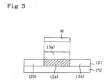
- the adhesion of the pressure-sensitive adhesive layer (2) to the die-bonding adhesive layer (3) is different between a region (2a) corresponding to the work-attaching region (3a) in the die-bonding adhesive layer (3)and a region (2b) corresponding to a part or the whole of the other region (3b), and satisfies the relationship the adhesion of the pressure-sensitive adhesive layer (2a) is lower than the adhesion of the pressure-sensitive adhesive layer (2b).
- the dicing/die-bonding film (1) of this invention comprises a pressure-sensitive adhesive layer (2) on a supporting base material (1) and a die-bonding adhesive layer (3) in a releasable manner on the pressure-sensitive adhesive layer (2).
- the adhesion of regions (2a, 2b) corresponding to the work-attaching region (3a) and the other region (3b) respectively in the die-bonding adhesive layer (3) is designed such that the adhesion of the pressure-sensitive adhesive layer (2a) is lower than the adhesion of the pressure-sensitive adhesive layer (2b). That is, the pressure-sensitive adhesive layer (2b) adheres suitably to the adhesive layer (3) during dicing step or expanding step, to prevent the adhesive layer (3) from being released from the pressure-sensitive adhesive layer (2).
- an adhesion of the work-attaching region (3a) in the die-bonding adhesive layer (3) to the work and to the pressure-sensitive adhesive layer (2a) satisfies the relationship: the adhesion to the work is higher than the adhesion to the pressure-sensitive adhesive layer (2a).
- the die-bonding adhesive layer (3) arranged on the chipped work after dicing can be easily released from the pressure-sensitive adhesive layer (2a).
- the part of the region (3b) other than the work-attaching region (3a) in the die-bonding adhesive layer (3) can be used as a dicing ring-attaching region (3b').
- an adhesion of the dicing ring-attaching region (3b') in the die-bonding adhesive layer (3) to the dicing ring and to the pressure-sensitive adhesive layer (2b') satisfies the relationship: the adhesion to the dicing ring is lower than the adhesion to the pressure-sensitive adhesive layer (2b').
- this invention relates to a dicing/die-bonding film comprising a pressure-sensitive adhesive layer (2) on a supporting base material (1) and a die-bonding adhesive layer (3) on the pressure-sensitive adhesive layer (2), wherein the die-bonding adhesive layer (3) is arranged as a work-attaching region (3a) on a part of the pressure-sensitive adhesive layer (2), and a region (2a) corresponding to the work-attaching region (3a) in the pressure-sensitive adhesive layer (2) and the other region (2b) are different in adhesion and satisfy the relationship: the adhesion of the pressure-sensitive adhesive layer (2a) is lower than the adhesion of the pressure-sensitive adhesive layer (2b).
- the die-bonding adhesive layer (3a) arranged on the chipped work after dicing can be easily released from the pressure-sensitive adhesive layer (2a).
- Figs. 1 and 2 are sectional views of the dicing/die-bonding film (1) of this invention that comprises a pressure-sensitive adhesive layer (2) on a supporting base material (1) and a die-bonding adhesive layer (3) on the pressure-sensitive adhesive layer (2).
- the regions (2a, 2b) in the pressure-sensitive adhesive layer (2) are designed such that the releasability from the die-bonding adhesive layer (3) is in the relationship: the releasability of the interface (A) corresponding to the work-attaching region (3a) is higher than the releasability of the interface (B) corresponding to the other region (3b).
- the pressure-sensitive adhesive layer (2a) corresponds to the work-attaching region (3a) in the die-bonding adhesive layer (3), and the pressure-sensitive adhesive layer (2b) corresponds to the other region (3b).
- the supporting base material (1) serves as a material conferring strength on the dicing/die-bonding film.
- Examples thereof include polyolefins such as low-density polyethylene, linear polyethylene, medium-density polyethylene, high-density polyethylene, super-low-density polyethylene, a random copolymer of polypropylene, a block copolymer of polypropylene, homopolypropylene, polybutene and polymethyl pentene; an ethylene-vinyl acetate copolymer, ionomer resin, an ethylene/(meth)acrylic acid copolymer, an ethylene/(meth)acrylate (random, alternating) copolymer, an ethylene-butene copolymer, an ethylene-hexene copolymer, polyurethane, polyesters such as polyethylene terephthalate and polyethylene naphthalene, polycarbonate, polyimide, polyether ether ketone, polyimide, polyether im
- the material of the supporting base material may be the same material or a suitable mixture of different materials, and if necessary a blend of several materials can also be used. Further, the supporting base material may be provided thereon with an electroconductive deposit of 30 to 500 ⁇ in thickness composed of a metal, an alloy or oxide thereof in order to confer antistatic performance.
- the supporting base material may be composed of a single or two or more layers.
- the thickness of the supporting base material (1) can be suitably determined without particular limitation, but is generally about 5 to 200 ⁇ m.
- the adhesive layer (3) or (3a) is stuck on the pressure-sensitive adhesive layer (2a) whose adhesion was reduced, the interface between the pressure-sensitive adhesive layer (2a) and the adhesive layer (3a) is inherently easily separated at the pickup step.
- the region not irradiated with radiations has sufficient adhesion, and forms the pressure-sensitive adhesive layer (2b).
- the pressure-sensitive adhesive layer (2b) made of the uncured radiation-curing pressure-sensitive adhesive adheres to the adhesive layer (3), thus maintaining retaining force at the dicing step.
- the radiation-curing pressure-sensitive adhesive can, with good balance between adhesion and release, support the die-bonding adhesive layer (3) for fixing a chipped work (semiconductor chip etc.) to an adherend (referred to as semiconductor element) such as a substrate and a chipped work.
- the pressure-sensitive adhesive layer (2b) can fix a wafer ring etc.
- the radiation-curing pressure-sensitive adhesive used in formation of the pressure-sensitive adhesive layer (2) can be used without particular limitation insofar as it has radiation-curing functional groups such as carbon-carbon double bonds and simultaneously shows adhesion.
- the pressure-sensitive adhesive can suitably use an external crosslinking agent for increasing the number-average molecular weight of the acrylic polymer etc. as the base polymer.
- a specific means of an external crosslinking method includes a method of reacting monomers by adding a crosslinking agent such as polyisocyanate compound, epoxy compound and aziridine compound, melamine-based crosslinking agent.
- the amount of the crosslinking agent used is suitably determined according to balancing with the base polymer to be crosslinked and the use of the pressure-sensitive adhesive.
- the external crosslinking agent is compounded in an amount of preferably 5 parts or less by weight, more preferably 0.1 to 5 parts by weight, based on 100 parts by weight of the base polymer.
- the pressure-sensitive adhesive may include various kinds of conventional additives such as tackifier, antioxidants etc.
- the radiation-curing pressure-sensitive adhesive includes not only the above-described addition-type radiation curing pressure-sensitive adhesives, but also internal-type radiation-curing pressure-sensitive adhesives using a base polymer having carbon-carbon double bonds in side chains or main chain of the polymer or at the end of the main chain.
- the internal-type radiation-curing pressure-sensitive adhesive is preferable because it does not requires incorporation of low-molecular components such as oligomer components or does not contain a large amount of oligomer components, thus enabling formation of a pressure-sensitive adhesive layer having a stable layer structure without movement with time of the oligomer components etc. in the pressure-sensitive adhesive.
- the method of introducing carbon-carbon double bonds into the acrylic polymer is not particularly limited and various methods can be used, but it is easy in molecular design to introduce carbon-carbon double bonds into side chains of the polymer.
- Combinations of these functional groups include, for example, a carboxylic acid group and an epoxy group, a carboxylic acid group and an aziridyl group, and a hydroxyl group and an isocyanate group.
- a combination of a hydroxyl group and an isocyanate group is preferable for easy monitoring of the reaction.
- the functional groups may be present in either the acrylic polymer or the above compound, and it is preferable in the above preferable combination that the acrylic polymer has a hydroxyl group, and the above compound has an isocyanate group.
- the isocyanate compound having carbon-carbon double bonds includes, for example, methacryloyl isocyanate, 2-methacryloyl oxyethyl isocyanate, m-isopropenyl- ⁇ , ⁇ -dimethylbenzyl isocyanate etc.
- the acrylic polymer use is made of a polymer prepared by copolymerizing the above-exemplified hydroxyl group-containing monomer or an ether compound such as 2-hydroxy ethyl vinyl ether, 4-hydroxy butyl vinyl ether or diethylene glycol monovinyl ether.
- the base polymer having carbon-carbon double bonds can be singly used.
- the radiation-curing monomer components and oligomer components can also be compounded to such a degree that the characteristics are not deteriorated.
- the amount of the radiation-curing oligomer components is usually in the range of 0 to 30 parts by weight, preferably 0 to 10 parts by weight, based on 100 parts by weight of the base polymer.
- the radiation-curing pressure-sensitive adhesive is blended with a photopolymerization initiator.
- the photopolymerization initiator includes, for example, ⁇ -ketol compounds such as 4-(2-hydroxyethoxy)phenyl(2-hydroxy-2-propyl)ketone, ⁇ -hydroxy- ⁇ , ⁇ '-dimethyl acetophenone, 2-methyl-2-hydroxypropiophenone and 1-hydroxycyclohexyl phenyl ketone; acetophenone compounds such as methoxy acetophenone, 2,2-dimethoxy-2-phenyl acetophenone, 2,2-diethoxy acetophenone and 2-methyl-1-[4-(methylthio)-phenyl)-2-morpholinopropane-1; benzoin ether compounds such as benzoin ethyl ether, benzoin isopropyl ether and anisoin methyl ether; ketal compounds such as benzyl dimethyl ketal; aromatic sulfate, benzyl di
- the radiation-curing pressure-sensitive adhesive include pressure-sensitive adhesive disclosed in JP-A 60-196956, for example rubber-based pressure-sensitive adhesive and acrylic pressure-sensitive adhesive containing an addition-polymerizable compound having two or more unsaturated bonds or a photopolymerizable compound such as alkoxy silane having an epoxy group and a photopolymerizable initiator such as a carbonyl compound, organic sulfur compound, peroxide, amine, or onium salt-based compound.
- the radiation-curing pressure-sensitive adhesive layer (2) can also contain a compound to be colored by irradiation with radiations.
- a compound to be colored by irradiation with radiations By incorporating the compound colored by irradiation with radiations into the radiation-curing pressure-sensitive adhesive (2), only a region irradiated with radiations can be colored. That is, the pressure-sensitive adhesive layer (2a) corresponding to the work-attaching region (3a) can be colored. Accordingly, whether the pressure-sensitive adhesive layer (2) has been irradiated with radiations can be immediately judged with the naked eye, and the work-attaching region (3a) can be easily recognized to facilitate attachment to a work. Further, when the resulting semiconductor element is detected by an optical sensor etc., the detection accuracy is improved, thus preventing erroneous working in pickup of the semiconductor element.
- the compounds to be colored by irradiation with radiations are colorless or light-colored before irradiation with radiations, but are colored by irradiation with radiations.
- Preferable examples of such compounds include leuco dyes.
- the leuco dyes used are preferably conventional dyes based on triphenyl methane, fluoran, phenothiazine, auramine and spiropyran.
- the compound to be colored with irradiation with radiations may be first dissolved in an organic solvent etc. and then incorporated into the radiation-curing pressure-sensitive adhesive, or may be first pulverized finely and then incorporated into the pressure-sensitive adhesive.
- the ratio of this compound used is 10% or less by weight, preferably 0.01 to 10% by weight, more preferably 0.5 to 5% by weight, based on the pressure-sensitive adhesive layer (2).
- the ratio of the compound is preferably 0.01% or more by weight.
- the pressure-sensitive adhesive layer (2) is arranged such that the adhesion of the pressure-sensitive adhesive layer (2a) is lower than the adhesion of the pressure-sensitive adhesive layer (2b).
- the adhesion to the die-bonding adhesive layer (3) is determined such that the releasability of the interface (A) is higher than the releasability of the interface (B).
- the adhesion of the pressure-sensitive adhesive layer (2a) to an SUS304 plate (#2000 polishing) as an adherend is lower than the adhesion of the pressure-sensitive adhesive layer (2b) to the plate.
- the surface of the radiation-curing pressure-sensitive adhesive layer (2) is preferably shielded from oxygen (air) by some methods. Such methods involve covering the surface of the pressure-sensitive adhesive layer (2) with a separator or irradiating with radiations such as UV rays etc. in a nitrogen atmosphere.
- thermoplastic die adhesive includes, for example, saturated polyester resin, thermoplastic polyurethane-based resin, amide-based resin (nylon-based resin), imide-based resin etc.
- the thermosetting resin includes, for example, epoxy resin, unsaturated polyester-based resin, thermosetting acrylic resin, phenol resin etc.
- the thermosetting resin is preferably a thermosetting resin in B-stage, which was desolvated and formed into a sheet. A mixture in B-stage of the thermosetting resin and thermoplastic resin can also be used.
- resins for examples those having a high glass transition temperature based on silicone, rubber, urethane, imide and acryl can also be used as the die adhesive.
- the die-bonding adhesive layer (3) may have a two- or more multi-layer structure by suitably combining thermoplastic resins different in glass transition temperature or thermosetting resins different in thermosetting temperature. Because water for cutting is used in the step of dicing the work (semiconductor wafer etc.), the die-bonding adhesive layer (3) adsorbs moisture to attain a water content higher than in an ordinary state. When the adhesive layer (3) having such a high water content is allowed to adhere to a substrate etc., water vapor may be retained in the interface of the adhesive at the after-cure stage to cause lifting.
- the dicing/die-bonding films (1) and (2) comprising the pressure-sensitive adhesive layer (2) on the supporting base material (1) and the die-bonding adhesive layer (3) on the pressure-sensitive adhesive layer (2) are obtained in this manner.
- the dicing/die-bonding films (1) and (2) can be endowed with antistatic performance for the purpose of preventing generation of static electricity upon sticking or release, or breakage of circuits by works (semiconductor wafer etc.) electrified with such static electricity.
- Antistatic performance can be given in a suitable system, for example by adding an antistatic agent or an electroconductive material to the supporting base material (1), the pressure-sensitive adhesive layer (2) or the adhesive layer (3) or by providing the supporting base material (1) with an electrostatic layer made of a charge-transferring complex or a metallic film.
- This system is preferably a system not generating contaminating ions that may denature semiconductor wafers.
- the electroconductive material (electroconductive filers) incorporated for the purpose of conferring electrical conductivity, thermal conductivity etc. includes spherical, needle or flaky metal powders of silver, aluminum, gold, copper, nickel, electroconductive alloys etc., metal oxides such as alumina, amorphous carbon black, graphite etc.
- the adhesion of the pressure-sensitive adhesive layer (2) to the die-bonding adhesive layer (3) is designed such that the adhesion of the pressure-sensitive adhesive layer (2a) is lower than the adhesion of the pressure-sensitive adhesive layer (2b).
- the adhesion of the pressure-sensitive adhesive layer (2a) is preferably not higher than 0.5 N/20 mm, more preferably 0.01 to 0.42 N/20 mm, still more preferably 0.01 to 0.35 N/20 mm from the viewpoint of retention of a wafer or recovery of formed chips.
- the adhesion of the pressure-sensitive adhesive layer (2b) is preferably about 0.5 to 20 N/20 mm. Even if the pressure-sensitive adhesive layer (2a) has low peel adhesion, the adhesion of the pressure-sensitive adhesive layer (2b) can prevent chips from being scattered, and can demonstrate sufficient retention for processing of wafers.
- the region (2a) corresponding to the work-attaching region (3a) and the other region (2b) in the pressure-sensitive adhesive layer (2) are designed such that the adhesion of the pressure-sensitive adhesive layer (2a) is lower than the adhesion of the pressure-sensitive adhesive layer (2b).
- the adhesion of the pressure-sensitive adhesive layer (2a) to the work-attaching region (3a) is not higher than 0.5 N/20 mm, more preferably 0.01 to 0.42 N/20 mm, and still more preferably 0.01 to 0.35 N/20 mm.
- the adhesion of the work-attaching region (3a) to the pressure-sensitive adhesive layer (2a) is not higher than 0.5 N/20 mm, more preferably 0.01 to 0.42 N/20 mm, and still more preferably 0.01 to 0.35 N/20 mm.
- the adhesion of the work-attaching region (3a) to the work is not higher than 10 to 50 N/20 mm, more preferably 10 to 30 N/20 mm, from the viewpoint of pickup and reliability at the time of dicing, pickup, and die-bonding.
- the adhesion of the dicing ring-attaching region (3b') in the die-bonding adhesive layer (3) to the work and to the pressure-sensitive adhesive layer (2b') is designed preferably such that the adhesion to the dicing ring is lower than the adhesion to the pressure-sensitive adhesive layer (2b').
- the adhesion to the dicing ring is regulated suitably depending on the type of the dicing ring.
- the adhesion of the die-bonding adhesive layer (3) to the pressure-sensitive adhesive layer (2b') is preferably about 0.5 to 20 N/20 mm.
- the adhesion of the die-bonding adhesive layer (3) to the dicing ring is preferably 0.3 to 5 N/20 mm, more preferably 0.5 to 5 N/20 mm, from the view point of workability at the time of dicing and die-bonding.
- the die-bonding adhesive layers (3) and (3a) may be protected with a separator (not shown in drawings). That is, a separator may be arbitrarily arranged. The separator functions as a protecting material protecting the die-bonding adhesive layers (3) and (3a). Further, the separator can also be used as a supporting base material for transferring the die-bonding adhesives (3) and (3a) to the pressure-sensitive adhesive layer (2). The separator is removed just before a work is stuck on the die-bonding adhesive layer (3) or (3a) in the dicing/die-bonding film (1) or (2).
- the separator includes a polyethylene or polypropylene film or a plastic film and paper coated with a releasing agent such as fluorine releasing agent or a long chain alkyl acrylate releasing agent.
- the chipped work together with the die-bonding adhesive layer (3a) is released from the pressure-sensitive adhesive layer (2a).
- the chipped work thus picked up is adhesive-bonded via the die-bonding adhesive layer (3a) to a semiconductor element as an adherend.
- the semiconductor element includes a lead frame, a TAB film, a substrate or a separately prepared chipped work.
- the adherend may be a deformed adherend to be easily deformed, or a hardly deformable non-deformed adherent (semiconductor wafer etc.).
- the adherend is preferably a semiconductor wafer.
- the adhesive layer (3) or (3a) is thermosetting, the work is adhesive-bonded to an adherend by thermosetting, to improve heat resistance.
- the chipped work adhesive-bonded to a substrate via the adhesive layers (3a) can be subjected to a reflow process.
- UV irradiation unit NUV irradiation unit
- compositions for die-bonding adhesives (A) to (C) were compounded in the ratios shown in the table to prepare compositions for die-bonding adhesives (A) to (C), and each composition was mixed with and dissolved in toluene.
- the mixed solution was applied onto a polyester film (separator) treated with a releasing agent. Then, the polyester film coated with the mixed solution was dried at 120°C to remove the toluene, whereby each of the die-bonding adhesive layers A to C of 20 ⁇ m in thickness in the B-stage on the polyester film were obtained.
- the above radiation-curing acrylic pressure-sensitive adhesive solution was applied onto a polyethylene film of 60 ⁇ m in thickness as the supporting base material and dried to form a pressure-sensitive adhesive layer of 20 ⁇ m in thickness.
- the resulting product is referred to as pressure-sensitive adhesive film (A).
- Only a wafer-attaching region of the pressure-sensitive adhesive layer in the pressure-sensitive adhesive film (A) was irradiated with UV rays in a total dose of 500 mJ/cm 2 to give a film having the pressure-sensitive adhesive layer whose wafer-attaching region had been cured by UV rays.
- the above die-bonding adhesive layer (A) was transferred onto the pressure-sensitive adhesive layer of the pressure-sensitive adhesive film (A), to give a dicing/die-bonding film.
- a dicing/die-bonding film was prepared in the same manner as in Example 1 except that the die-bonding adhesive (B) was used in place of the die-bonding adhesive (A) in Example 1.
- the above radiation-curing acrylic pressure-sensitive adhesive solution was applied onto a polyethylene film of 80 ⁇ m in thickness as the supporting base material and dried to form a pressure-sensitive adhesive layer of 5 ⁇ m in thickness.
- the resulting product is referred to as pressure-sensitive adhesive film (B).
- Only a wafer-attaching region of the pressure-sensitive adhesive layer in the pressure-sensitive adhesive film (B) was irradiated with 500 mJ/cm 2 UV rays to give a film having the pressure-sensitive adhesive layer whose wafer-attaching region had been cured by UV rays.
- the above die-bonding adhesive layer (B) was transferred onto the pressure-sensitive adhesive layer of the pressure-sensitive adhesive film (B), to give a dicing/die-bonding film.
- a dicing/die-bonding film was prepared in the same manner as in Example 3 except that the die-bonding adhesive layer (C) was used in place of the die-bonding adhesive (B) in Example 3.
- a dicing/die-bonding film was prepared in the same manner as in Example 3 except that the die-bonding adhesive layer (A) was used in place of the die-bonding adhesive (B) in Example 3.
- a dicing/die-bonding film was prepared in the same manner as in Example 1 except that the pressure-sensitive adhesive layer on the t pressure-sensitive adhesive film (A) was not irradiated with UV rays, and also that the die-bonding adhesive layer (A) after being transferred onto the pressure-sensitive adhesive layer was irradiated with 500 mJ/cm 2 UV rays.
- the pressure-sensitive adhesive film used in each example was irradiated in the side of the supporting base material with UV rays (500 mJ/cm 2 ) and cut into rectangular strips of 10 mm in width. Separately, the die-bonding adhesive layer used in each example was stuck onto a 6-inch silicon wafer (ground surface #2000) placed on a hot plate at 40°C.
- Each of the pressure-sensitive adhesive films A and B was cut into rectangular strips of 10 mm in thickness. Thereafter, the pressure-sensitive adhesive film (10 mm) was stuck onto an SUS304 plate (#2000 polishing) at room temperature (23°C) and left for 30 minutes in a room-temperature atmosphere, and the adhesion of the pressure-sensitive adhesive film when peeled off at a peel angle of 90° in a thermostat chamber at 23°C was measured (stress rate of the pressure-sensitive adhesive film, 300 mm/min.).
- Full-dicing was carried out in the same manner as described above except that the size of the square chips was changed into 5 ⁇ 5 mm, 10 ⁇ 10 mm, and 15 ⁇ 15 mm respectively. Thereafter, the silicon chips (chipped wafer) were picked up in a system for raising the side of the supporting base material by a needle. " ⁇ ” was given to successful pickup, and "x” was given to unsuccessful pickup.
- the dicing/die-bonding film having a pressure-sensitive adhesive layer between a supporting base material and an adhesive layer wherein the adhesion between the adhesive layer and the pressure-sensitive adhesive layer is lower in the wafer-attaching region than in the other region (region onto which a wafer is not stuck) has the adhesion thereof to a dicing ring without failure in dicing, and chips of various sizes can be picked up well.
Landscapes
- Chemical & Material Sciences (AREA)
- Organic Chemistry (AREA)
- Dicing (AREA)
- Adhesives Or Adhesive Processes (AREA)
- Adhesive Tapes (AREA)
- Die Bonding (AREA)
Applications Claiming Priority (2)
| Application Number | Priority Date | Filing Date | Title |
|---|---|---|---|
| JP2002299930A JP4107417B2 (ja) | 2002-10-15 | 2002-10-15 | チップ状ワークの固定方法 |
| JP2002299930 | 2002-10-15 |
Publications (2)
| Publication Number | Publication Date |
|---|---|
| EP1411547A2 true EP1411547A2 (de) | 2004-04-21 |
| EP1411547A3 EP1411547A3 (de) | 2004-09-22 |
Family
ID=32040779
Family Applications (1)
| Application Number | Title | Priority Date | Filing Date |
|---|---|---|---|
| EP03023536A Withdrawn EP1411547A3 (de) | 2002-10-15 | 2003-10-15 | Film zum Schneiden und Zerteilen und Verfahren zur Befestigung von Halbleiterchips sowie Halbleiteranordnung |
Country Status (7)
| Country | Link |
|---|---|
| US (4) | US7060339B2 (de) |
| EP (1) | EP1411547A3 (de) |
| JP (1) | JP4107417B2 (de) |
| KR (1) | KR101057884B1 (de) |
| CN (1) | CN100358126C (de) |
| SG (1) | SG111163A1 (de) |
| TW (1) | TWI307545B (de) |
Cited By (12)
| Publication number | Priority date | Publication date | Assignee | Title |
|---|---|---|---|---|
| EP1482546A3 (de) * | 2003-05-29 | 2005-03-02 | Nitto Denko Corporation | Film pour le découpage et le montage et méthode de fixation de puces semiconductrices et composant semiconducteur |
| US7060339B2 (en) | 2002-10-15 | 2006-06-13 | Nitto Denko Corporation | Dicing/die-bonding film, method of fixing chipped work and semiconductor device |
| EP1583144A3 (de) * | 2004-03-17 | 2006-07-26 | Nitto Denko Corporation | Klebefilm zum Schneiden und Befestigung von Halbleiterchips |
| US7309925B2 (en) | 2003-12-26 | 2007-12-18 | Nitto Denko Corporation | Dicing die-bonding film |
| EP2090633A1 (de) * | 2008-02-18 | 2009-08-19 | Nitto Denko Corporation | Klebefilm zum Schneiden von Halbleiterchips |
| EP1890326A3 (de) * | 2006-08-18 | 2009-10-21 | Princo Corp. | Struktur aus einem Substrat mit integriertem IC und einem Träger sowie Herstellungsverfahren für eine solche Struktur |
| EP2063460A4 (de) * | 2006-09-12 | 2011-08-03 | Nitto Denko Corp | Zerteilungs-/chipbondfilm |
| US7993973B2 (en) | 2005-12-22 | 2011-08-09 | Princo Corp. | Structure combining an IC integrated substrate and a carrier, and method of manufacturing such structure |
| EP2471884A1 (de) * | 2010-12-28 | 2012-07-04 | Nitto Denko Corporation | Strahlenhärtbare Haftzusammensetzung und Haftfolie |
| US8465615B2 (en) | 2004-10-14 | 2013-06-18 | Hitachi Chemical Company, Ltd. | Adhesive sheet and method for manufacturing the same, semiconductor device manufacturing method and semiconductor device |
| US8617928B2 (en) | 2008-01-18 | 2013-12-31 | Nitto Denko Corporation | Dicing/die bonding film |
| US9327418B2 (en) | 2011-09-16 | 2016-05-03 | Hitachi Chemical Company, Ltd. | Adhesive film |
Families Citing this family (55)
| Publication number | Priority date | Publication date | Assignee | Title |
|---|---|---|---|---|
| US7641966B2 (en) * | 1999-06-14 | 2010-01-05 | Nitto Denko Corporation | Re-release adhesive and re-release adhesive sheet |
| KR101170845B1 (ko) * | 2003-02-05 | 2012-08-02 | 후루카와 덴키 고교 가부시키가이샤 | 다이싱 다이본딩 테이프 |
| KR100885099B1 (ko) * | 2003-12-15 | 2009-02-20 | 후루카와 덴키 고교 가부시키가이샤 | 웨이퍼 가공용 테이프 및 그 제조방법 |
| KR100590198B1 (ko) * | 2004-03-25 | 2006-06-19 | 엘에스전선 주식회사 | 수축성 이형필름을 갖는 다이싱 필름 및 이를 이용한반도체 패키지 제조방법 |
| US20050227064A1 (en) * | 2004-04-01 | 2005-10-13 | Hwail Jin | Dicing die bonding film |
| US20070003758A1 (en) * | 2004-04-01 | 2007-01-04 | National Starch And Chemical Investment Holding Corporation | Dicing die bonding film |
| US20050255632A1 (en) * | 2004-05-13 | 2005-11-17 | Stack Devices Corp. | Method of fabricating stacked semiconductor device |
| TWI273662B (en) * | 2004-12-06 | 2007-02-11 | Advanced Semiconductor Eng | Method for chip bonding |
| JP4800694B2 (ja) * | 2005-07-26 | 2011-10-26 | 日東電工株式会社 | ダイシング・ダイボンドフィルム |
| WO2008010547A1 (en) * | 2006-07-19 | 2008-01-24 | Sekisui Chemical Co., Ltd. | Dicing/die-bonding tape and method for manufacturing semiconductor chip |
| JP4430085B2 (ja) | 2007-03-01 | 2010-03-10 | 日東電工株式会社 | ダイシング・ダイボンドフィルム |
| US8232185B2 (en) * | 2007-04-05 | 2012-07-31 | Hitachi Chemical Company, Ltd. | Method for manufacturing semiconductor chip, adhesive film for semiconductor, and composite sheet using the film |
| KR101273871B1 (ko) * | 2007-04-19 | 2013-06-11 | 세키스이가가쿠 고교가부시키가이샤 | 다이싱ㆍ다이본딩 테이프 및 반도체칩의 제조 방법 |
| JP4717051B2 (ja) * | 2007-11-08 | 2011-07-06 | 日東電工株式会社 | ダイシング・ダイボンドフィルム |
| JP4717052B2 (ja) * | 2007-11-08 | 2011-07-06 | 日東電工株式会社 | ダイシング・ダイボンドフィルム |
| KR101047923B1 (ko) | 2007-12-27 | 2011-07-08 | 주식회사 엘지화학 | 버 특성 및 신뢰성이 우수한 다이싱 다이 본딩 필름 및반도체 장치 |
| JP4717086B2 (ja) * | 2008-01-18 | 2011-07-06 | 日東電工株式会社 | ダイシング・ダイボンドフィルム |
| JP2009242605A (ja) * | 2008-03-31 | 2009-10-22 | Lintec Corp | 粘接着剤組成物、粘接着シートおよび半導体装置の製造方法 |
| JP4801127B2 (ja) * | 2008-09-01 | 2011-10-26 | 日東電工株式会社 | ダイシング・ダイボンドフィルムの製造方法 |
| JP5319993B2 (ja) * | 2008-09-10 | 2013-10-16 | 積水化学工業株式会社 | ダイシング−ダイボンディングテープ及び半導体チップの製造方法 |
| JP5275834B2 (ja) * | 2009-02-04 | 2013-08-28 | 古河電気工業株式会社 | ウエハ加工用フィルム及びウエハ加工用フィルムを用いて半導体装置を製造する方法 |
| JP2009111431A (ja) * | 2009-02-16 | 2009-05-21 | Nitto Denko Corp | ウェハのダイシング方法、半導体装置及びその製造方法、回路基板並びに電子機器 |
| JP2010219086A (ja) * | 2009-03-13 | 2010-09-30 | Furukawa Electric Co Ltd:The | ウエハ加工用フィルム及びウエハ加工用フィルムを用いて半導体装置を製造する方法 |
| JP5561949B2 (ja) * | 2009-04-08 | 2014-07-30 | 日東電工株式会社 | 熱硬化型ダイボンドフィルム |
| CN105047597B (zh) | 2009-06-15 | 2018-04-03 | 日东电工株式会社 | 半导体背面用切割带集成膜 |
| JP2011018805A (ja) * | 2009-07-09 | 2011-01-27 | Sumitomo Bakelite Co Ltd | 半導体用フィルムおよび半導体装置の製造方法 |
| JP5143196B2 (ja) * | 2009-09-28 | 2013-02-13 | 日東電工株式会社 | 半導体装置用フィルム |
| JP5137937B2 (ja) * | 2009-12-16 | 2013-02-06 | 日東電工株式会社 | 半導体装置製造用耐熱性粘着シート、該シートに用いる粘着剤、及び該シートを用いた半導体装置の製造方法 |
| JP2011151362A (ja) | 2009-12-24 | 2011-08-04 | Nitto Denko Corp | ダイシングテープ一体型半導体裏面用フィルム |
| KR101019756B1 (ko) * | 2009-12-24 | 2011-03-09 | 제일모직주식회사 | 비자외선형 다이접착필름 및 제조방법 |
| JP4988815B2 (ja) * | 2009-12-25 | 2012-08-01 | 日東電工株式会社 | チップ保持用テープ、チップ状ワークの保持方法、チップ保持用テープを用いた半導体装置の製造方法、及び、チップ保持用テープの製造方法 |
| JP5438522B2 (ja) * | 2010-01-07 | 2014-03-12 | 積水化学工業株式会社 | ダイシング−ダイボンディングテープ及びその製造方法 |
| KR101083959B1 (ko) * | 2010-02-01 | 2011-11-16 | 닛토덴코 가부시키가이샤 | 반도체 장치 제조용 필름 및 반도체 장치의 제조 방법 |
| SG183334A1 (en) | 2010-03-09 | 2012-09-27 | Furukawa Electric Co Ltd | Wafer-processing film and method of manufacturing semiconductor device by using wafer-processing film |
| KR20120092694A (ko) * | 2010-03-31 | 2012-08-21 | 후루카와 덴키 고교 가부시키가이샤 | 반도체 웨이퍼 가공용 점착시트 |
| JP5439264B2 (ja) | 2010-04-19 | 2014-03-12 | 日東電工株式会社 | ダイシングテープ一体型半導体裏面用フィルム |
| JP5681374B2 (ja) | 2010-04-19 | 2015-03-04 | 日東電工株式会社 | ダイシングテープ一体型半導体裏面用フィルム |
| JP5546985B2 (ja) * | 2010-07-28 | 2014-07-09 | 日東電工株式会社 | 半導体装置製造用フィルム、半導体装置製造用フィルムの製造方法、及び、半導体装置の製造方法。 |
| KR101351615B1 (ko) * | 2010-12-13 | 2014-01-15 | 제일모직주식회사 | 반도체용 점접착시트 및 그의 제조 방법 |
| KR20120068453A (ko) * | 2010-12-17 | 2012-06-27 | 제일모직주식회사 | 다이싱 다이 본딩 필름 |
| JP5687897B2 (ja) * | 2010-12-28 | 2015-03-25 | 日東電工株式会社 | 放射線硬化型粘着剤組成物及び粘着シート |
| JP2012156292A (ja) * | 2011-01-26 | 2012-08-16 | Seiko Epson Corp | 基板の加工方法 |
| JP4904432B1 (ja) | 2011-03-01 | 2012-03-28 | 古河電気工業株式会社 | ウエハ加工用テープ |
| JP2013038405A (ja) * | 2011-07-08 | 2013-02-21 | Sumitomo Bakelite Co Ltd | ダイシングテープ一体型接着シート、半導体装置、多層回路基板及び電子部品 |
| KR101939636B1 (ko) * | 2011-09-30 | 2019-01-17 | 린텍 코포레이션 | 보호막 형성층을 갖는 다이싱 시트 및 칩의 제조 방법 |
| EP2791967A4 (de) | 2011-12-15 | 2015-08-05 | Henkel IP & Holding GmbH | Verfahren zur herstellung eines haftfilms in einer vorgeschnittenen halbleiterwaferform auf einem dicing-band |
| JP5950838B2 (ja) * | 2012-03-07 | 2016-07-13 | 古河電気工業株式会社 | 粘着テープ |
| JP5591859B2 (ja) * | 2012-03-23 | 2014-09-17 | 株式会社東芝 | 基板の分離方法及び分離装置 |
| WO2014141276A2 (en) * | 2013-03-14 | 2014-09-18 | Stratasys Ltd. | Polymer based molds and methods of manufacturing there of |
| JP6190671B2 (ja) * | 2013-09-05 | 2017-08-30 | 古河電気工業株式会社 | ダイシング用粘着テープおよび半導体装置の製造方法 |
| KR102171423B1 (ko) * | 2013-10-21 | 2020-10-29 | 린텍 가부시키가이샤 | 수지막 형성용 시트 |
| JP7280661B2 (ja) * | 2017-12-28 | 2023-05-24 | 日東電工株式会社 | ダイシングダイボンドフィルム |
| JP7409029B2 (ja) * | 2019-11-15 | 2024-01-09 | 株式会社レゾナック | 半導体装置の製造方法、並びにダイシング・ダイボンディング一体型フィルム及びその製造方法 |
| JP7409030B2 (ja) * | 2019-11-15 | 2024-01-09 | 株式会社レゾナック | ダイシング・ダイボンディング一体型フィルム及びその製造方法、並びに半導体装置の製造方法 |
| US12552975B2 (en) | 2020-03-06 | 2026-02-17 | Tredegar Surface Protection, Llc | Carrier film for semi-conductor wafer processing |
Family Cites Families (162)
| Publication number | Priority date | Publication date | Assignee | Title |
|---|---|---|---|---|
| IE55238B1 (en) | 1983-08-03 | 1990-07-04 | Nat Starch Chem Corp | Carrier film with conductive adhesive for dicing of semiconductor wafers |
| US4961804A (en) * | 1983-08-03 | 1990-10-09 | Investment Holding Corporation | Carrier film with conductive adhesive for dicing of semiconductor wafers and dicing method employing same |
| US4664739A (en) * | 1983-12-19 | 1987-05-12 | Stauffer Chemical Company | Removal of semiconductor wafers from dicing film |
| CA1222071A (en) | 1984-01-30 | 1987-05-19 | Joseph A. Aurichio | Conductive die attach tape |
| JPH0616524B2 (ja) | 1984-03-12 | 1994-03-02 | 日東電工株式会社 | 半導体ウエハ固定用接着薄板 |
| JPS60196955A (ja) | 1984-03-19 | 1985-10-05 | Toko Inc | 誘電体分離基板の製造方法 |
| FR2580416B1 (fr) * | 1985-04-12 | 1987-06-05 | Radiotechnique Compelec | Procede et dispositif pour fabriquer une carte d'identification electronique |
| JPS61263136A (ja) | 1985-05-15 | 1986-11-21 | Nitto Electric Ind Co Ltd | 薄板物品の支持テ−ブル |
| US4687693A (en) * | 1985-06-13 | 1987-08-18 | Stauffer Chemical Company | Adhesively mountable die attach film |
| JPS6279649A (ja) | 1985-10-03 | 1987-04-13 | Mitsui Toatsu Chem Inc | 半導体ダイシング方法 |
| JPH01268131A (ja) | 1988-04-20 | 1989-10-25 | Nitto Denko Corp | 半導体ウエハの保護部材 |
| JP2678655B2 (ja) | 1989-03-20 | 1997-11-17 | 日東電工株式会社 | 半導体チップ固着キャリヤの製造方法及びウエハ固定部材 |
| JPH02265258A (ja) | 1989-04-05 | 1990-10-30 | Fujitsu Ltd | ダイシング装置 |
| DE69001797T2 (de) * | 1989-12-08 | 1994-01-27 | Sumitomo Electric Industries | Aufnahmeverfahren und -apparat für einen chipähnlichen Teil. |
| JPH0442555A (ja) | 1990-06-08 | 1992-02-13 | Sumitomo Electric Ind Ltd | チップ状部品のピックアップ装置とピックアップ方法 |
| JPH0578629A (ja) * | 1991-09-18 | 1993-03-30 | Furukawa Electric Co Ltd:The | 放射線硬化性粘着テープ |
| JPH05179211A (ja) | 1991-12-30 | 1993-07-20 | Nitto Denko Corp | ダイシング・ダイボンドフイルム |
| EP0571649A1 (de) | 1992-05-26 | 1993-12-01 | Nitto Denko Corporation | Unterstützungsfilm zum Schneiden und Befestigen von Halbleiterplättchen und dessen Verwendung in einem Verfahren zur Chipherstellung |
| DE4230784A1 (de) * | 1992-09-15 | 1994-03-17 | Beiersdorf Ag | Durch Strahlung partiell entklebendes Selbstklebeband (Dicing Tape) |
| SE470501B (sv) * | 1992-10-07 | 1994-06-06 | Ericsson Telefon Ab L M | Förfarande vid montering på ett substrat av en TAB-krets, varvid TAB-strukturens anslutningar utgörs av ett elektriskt ledande anslutningsmönster som framställts på en filmremsa och vilket är anslutet till TAB-strukturens halvledarkretsbricka |
| JP3348923B2 (ja) | 1993-07-27 | 2002-11-20 | リンテック株式会社 | ウェハ貼着用粘着シート |
| JPH07263382A (ja) | 1994-03-24 | 1995-10-13 | Kawasaki Steel Corp | ウェーハ固定用テープ |
| JP3521099B2 (ja) * | 1994-11-29 | 2004-04-19 | リンテック株式会社 | ダイシング用リングフレームへの接着剤の付着防止用粘着シートおよび該粘着シートを備えたウェハ加工用シート |
| JP3186510B2 (ja) * | 1995-06-09 | 2001-07-11 | 株式会社村田製作所 | 圧電共振部品及びその製造方法 |
| MY118036A (en) * | 1996-01-22 | 2004-08-30 | Lintec Corp | Wafer dicing/bonding sheet and process for producing semiconductor device |
| US6007920A (en) * | 1996-01-22 | 1999-12-28 | Texas Instruments Japan, Ltd. | Wafer dicing/bonding sheet and process for producing semiconductor device |
| TW340860B (en) | 1996-02-28 | 1998-09-21 | Nippon Chemicals Pharmaceutical Co Ltd | Liquid composition |
| US6328844B1 (en) * | 1996-07-15 | 2001-12-11 | Hitachi Chemical Company, Ltd. | Filmy adhesive for connecting circuits and circuit board |
| FI964640A7 (fi) | 1996-11-21 | 1998-07-28 | Nokia Multimedia Network Terminals Oy | Menetelmä osoitetietojen välittämiseksi |
| WO1998027442A1 (en) | 1996-12-02 | 1998-06-25 | Gordian Holding Corporation | Method for forming a radio frequency responsive target and apparatus for verifying the authenticity of same |
| US6312800B1 (en) * | 1997-02-10 | 2001-11-06 | Lintec Corporation | Pressure sensitive adhesive sheet for producing a chip |
| JPH10335271A (ja) | 1997-06-02 | 1998-12-18 | Texas Instr Japan Ltd | ウェハ貼着用シートおよび半導体装置の製造方法 |
| JP3955659B2 (ja) | 1997-06-12 | 2007-08-08 | リンテック株式会社 | 電子部品のダイボンディング方法およびそれに使用されるダイボンディング装置 |
| JP3097619B2 (ja) * | 1997-10-02 | 2000-10-10 | 日本電気株式会社 | 電界放射冷陰極の製造方法 |
| BE1011852A3 (fr) | 1998-03-24 | 2000-02-01 | Solvay | Procede de fabrication d'un oxiranne. |
| US6159827A (en) * | 1998-04-13 | 2000-12-12 | Mitsui Chemicals, Inc. | Preparation process of semiconductor wafer |
| US6140151A (en) * | 1998-05-22 | 2000-10-31 | Micron Technology, Inc. | Semiconductor wafer processing method |
| JP3669196B2 (ja) * | 1998-07-27 | 2005-07-06 | 日東電工株式会社 | 紫外線硬化型粘着シート |
| JP3784202B2 (ja) * | 1998-08-26 | 2006-06-07 | リンテック株式会社 | 両面粘着シートおよびその使用方法 |
| JP2000223446A (ja) * | 1998-11-27 | 2000-08-11 | Denso Corp | 半導体装置およびその製造方法 |
| JP3511929B2 (ja) * | 1999-01-25 | 2004-03-29 | 株式会社村田製作所 | 電子部品の製造方法、圧電共振部品の製造方法、電子部品及び圧電共振部品 |
| US7641966B2 (en) * | 1999-06-14 | 2010-01-05 | Nitto Denko Corporation | Re-release adhesive and re-release adhesive sheet |
| JP4392732B2 (ja) * | 2000-02-07 | 2010-01-06 | リンテック株式会社 | 半導体チップの製造方法 |
| JP2001240842A (ja) * | 2000-02-28 | 2001-09-04 | Nitto Denko Corp | 紫外線硬化型粘着剤組成物とその粘着シ―ト類 |
| US7054161B1 (en) * | 2000-04-19 | 2006-05-30 | James Stephen L | Slotted adhesive for die-attach in BOC and LOC packages |
| US6548327B2 (en) * | 2000-04-24 | 2003-04-15 | Interuniversitair Microelektronica Centrum, Vzw | Low cost electroless plating process for single chips and wafer parts and products obtained thereof |
| US6938783B2 (en) * | 2000-07-26 | 2005-09-06 | Amerasia International Technology, Inc. | Carrier tape |
| JP3605009B2 (ja) | 2000-08-03 | 2004-12-22 | 三洋電機株式会社 | 半導体装置の製造方法 |
| JP4109823B2 (ja) * | 2000-10-10 | 2008-07-02 | 株式会社東芝 | 半導体装置の製造方法 |
| JP2002158276A (ja) | 2000-11-20 | 2002-05-31 | Hitachi Chem Co Ltd | ウエハ貼着用粘着シートおよび半導体装置 |
| JP4780828B2 (ja) * | 2000-11-22 | 2011-09-28 | 三井化学株式会社 | ウエハ加工用粘着テープ及びその製造方法並びに使用方法 |
| JP2002226800A (ja) * | 2001-02-05 | 2002-08-14 | Hitachi Chem Co Ltd | 接着シート、その使用方法及び半導体装置 |
| JP4674836B2 (ja) | 2001-02-13 | 2011-04-20 | 日東電工株式会社 | ダイシング用粘着シート |
| JP2002256235A (ja) | 2001-03-01 | 2002-09-11 | Hitachi Chem Co Ltd | 接着シート、半導体装置の製造方法および半導体装置 |
| JP4839520B2 (ja) | 2001-03-22 | 2011-12-21 | 日立化成工業株式会社 | 接着シートならびに半導体装置およびその製造方法 |
| JP2002299378A (ja) * | 2001-03-30 | 2002-10-11 | Lintec Corp | 導電体付接着シート、半導体装置製造方法および半導体装置 |
| JP2002322436A (ja) * | 2001-04-25 | 2002-11-08 | Nitto Denko Corp | 被着物の加熱剥離方法及び被着物加熱剥離装置 |
| JP2003007646A (ja) | 2001-06-18 | 2003-01-10 | Nitto Denko Corp | ダイシング用粘着シートおよび切断片の製造方法 |
| JP2003056248A (ja) | 2001-08-09 | 2003-02-26 | Koito Mfg Co Ltd | 窓昇降装置 |
| JP4869517B2 (ja) * | 2001-08-21 | 2012-02-08 | リンテック株式会社 | 粘接着テープ |
| JP2004043762A (ja) | 2001-08-27 | 2004-02-12 | Hitachi Chem Co Ltd | 接着シート並びに半導体装置及びその製造方法 |
| US20030064579A1 (en) * | 2001-09-27 | 2003-04-03 | Masafumi Miyakawa | Surface protecting adhesive film for semiconductor wafer and protecting method for semiconductor wafer using said adhesive film |
| JP3969994B2 (ja) | 2001-10-16 | 2007-09-05 | 電気化学工業株式会社 | 電子部材用粘着テープ |
| US20030118071A1 (en) * | 2001-12-20 | 2003-06-26 | Eastman Kodak Company | Laser array and method of making same |
| JP2003206468A (ja) * | 2002-01-16 | 2003-07-22 | Asahi Kasei Corp | ウエハー固定用粘着剤ならびに加工方法 |
| JP2004231932A (ja) * | 2002-12-02 | 2004-08-19 | Nitto Denko Corp | 接着剤組成物、接着フィルムおよびこれを用いた半導体装置 |
| JP2003316031A (ja) | 2002-04-24 | 2003-11-06 | Mejiro Precision:Kk | 基準部形成装置 |
| US20050224978A1 (en) * | 2002-06-24 | 2005-10-13 | Kohichiro Kawate | Heat curable adhesive composition, article, semiconductor apparatus and method |
| JP2004063953A (ja) | 2002-07-31 | 2004-02-26 | Ube Ind Ltd | ダイシングテ−プ |
| JP2004095844A (ja) | 2002-08-30 | 2004-03-25 | Lintec Corp | ウエハダイシング・接着用シートおよび半導体装置の製造方法 |
| JP4107417B2 (ja) * | 2002-10-15 | 2008-06-25 | 日東電工株式会社 | チップ状ワークの固定方法 |
| JP4219660B2 (ja) * | 2002-11-18 | 2009-02-04 | 信越化学工業株式会社 | ウエハダイシング・ダイボンドシート |
| JP3966808B2 (ja) | 2002-12-03 | 2007-08-29 | 古河電気工業株式会社 | 粘接着テープ |
| JP4042555B2 (ja) | 2002-12-09 | 2008-02-06 | ソニー株式会社 | 半導体回路素子・光学素子混載ハイブリットモジュール及びその製造方法 |
| JP4245370B2 (ja) * | 2003-02-21 | 2009-03-25 | 大日本印刷株式会社 | 半導体装置の製造方法 |
| SG116533A1 (en) * | 2003-03-26 | 2005-11-28 | Toshiba Kk | Semiconductor manufacturing apparatus and method of manufacturing semiconductor device. |
| JP4361309B2 (ja) | 2003-04-17 | 2009-11-11 | 株式会社ディスコ | 半導体チップの製造方法 |
| WO2004096483A1 (ja) * | 2003-04-25 | 2004-11-11 | Nitto Denko Corporation | レーザー加工品の製造方法、およびそれに用いるレーザー加工用粘着シート |
| JP3710457B2 (ja) | 2003-05-22 | 2005-10-26 | 住友ベークライト株式会社 | ダイシングシート機能付きダイアタッチフィルム、それを用いた半導体装置の製造方法及び半導体装置 |
| JP4283596B2 (ja) | 2003-05-29 | 2009-06-24 | 日東電工株式会社 | チップ状ワークの固定方法 |
| JP2005005355A (ja) | 2003-06-10 | 2005-01-06 | Nitto Denko Corp | ダイシング・ダイボンドフィルム |
| US7008987B2 (en) * | 2003-06-10 | 2006-03-07 | Nitto Denko Corporation | Aqueous dispersion type pressure-sensitive adhesive composition, pressure-sensitive adhesive sheet, and pressure-sensitive adhesive rubber foam sheet using the sheet |
| JP4610168B2 (ja) * | 2003-08-06 | 2011-01-12 | スリーエム イノベイティブ プロパティズ カンパニー | 耐熱マスキングテープ |
| EP1584658B1 (de) * | 2003-09-26 | 2010-07-21 | DIC Corporation | Wässrige dispersion eines polyurethanharzes sowie diese enthaltende wässriger klebstoff für schuhe und wässrige grundierung |
| JP4405246B2 (ja) * | 2003-11-27 | 2010-01-27 | スリーエム イノベイティブ プロパティズ カンパニー | 半導体チップの製造方法 |
| JP2005159069A (ja) | 2003-11-27 | 2005-06-16 | Furukawa Electric Co Ltd:The | ダイシング用粘接着テープ |
| JP4472316B2 (ja) * | 2003-11-28 | 2010-06-02 | 日東電工株式会社 | 粘着テープ切断方法及び粘着テープ切断装置 |
| JP4125668B2 (ja) * | 2003-12-19 | 2008-07-30 | 日東電工株式会社 | 半導体装置の製造方法 |
| JP4275522B2 (ja) * | 2003-12-26 | 2009-06-10 | 日東電工株式会社 | ダイシング・ダイボンドフィルム |
| JP2005236082A (ja) * | 2004-02-20 | 2005-09-02 | Nitto Denko Corp | レーザーダイシング用粘着シート及びその製造方法 |
| JP4443962B2 (ja) * | 2004-03-17 | 2010-03-31 | 日東電工株式会社 | ダイシング・ダイボンドフィルム |
| KR100590198B1 (ko) * | 2004-03-25 | 2006-06-19 | 엘에스전선 주식회사 | 수축성 이형필름을 갖는 다이싱 필름 및 이를 이용한반도체 패키지 제조방법 |
| US20050227064A1 (en) * | 2004-04-01 | 2005-10-13 | Hwail Jin | Dicing die bonding film |
| US20070003758A1 (en) * | 2004-04-01 | 2007-01-04 | National Starch And Chemical Investment Holding Corporation | Dicing die bonding film |
| JP4716668B2 (ja) * | 2004-04-21 | 2011-07-06 | 日東電工株式会社 | 被着物の加熱剥離方法及び被着物加熱剥離装置 |
| JP4393934B2 (ja) | 2004-06-23 | 2010-01-06 | リンテック株式会社 | 半導体加工用粘着シート |
| US20060252234A1 (en) * | 2004-07-07 | 2006-11-09 | Lintec Corporation | Hardenable pressure sensitive adhesive sheet for dicing/die-bonding and method for manufacturing semiconductor device |
| JP4776189B2 (ja) | 2004-08-03 | 2011-09-21 | 古河電気工業株式会社 | ウエハ加工用テープ |
| USD549189S1 (en) * | 2004-09-21 | 2007-08-21 | Nitto Denko Corporation | Dicing die-bonding film |
| JP4704828B2 (ja) | 2004-09-29 | 2011-06-22 | 積水化学工業株式会社 | ウエハ貼着用粘着シート及びダイ接着用接着剤層付きicチップの製造方法 |
| JP4642436B2 (ja) * | 2004-11-12 | 2011-03-02 | リンテック株式会社 | マーキング方法および保護膜形成兼ダイシング用シート |
| US20080050583A1 (en) * | 2004-11-25 | 2008-02-28 | Teijin Dupont Films Japan Limited | Easily Adhesive Polyester Film and Film for Protecting Back Side of Solar Cell Using the Same |
| JP4704017B2 (ja) * | 2004-12-09 | 2011-06-15 | 日東電工株式会社 | 被着物の加熱剥離方法及び被着物加熱剥離装置 |
| JP4804007B2 (ja) * | 2005-01-13 | 2011-10-26 | 日東電工株式会社 | 粘着製品 |
| JP4699031B2 (ja) * | 2005-01-13 | 2011-06-08 | 日東電工株式会社 | 粘着製品および粘着製品用基材 |
| JP4873863B2 (ja) * | 2005-01-14 | 2012-02-08 | 日東電工株式会社 | レーザー加工品の製造方法及びレーザー加工用粘着シート |
| JP2006216773A (ja) | 2005-02-03 | 2006-08-17 | Lintec Corp | ダイシングシートおよび電子部品の製造方法 |
| JP4878869B2 (ja) * | 2005-04-08 | 2012-02-15 | 日東電工株式会社 | 発泡部材、発泡部材積層体及び発泡部材が用いられた電気・電子機器類 |
| JP4800778B2 (ja) * | 2005-05-16 | 2011-10-26 | 日東電工株式会社 | ダイシング用粘着シート及びそれを用いた被加工物の加工方法 |
| JP4800694B2 (ja) | 2005-07-26 | 2011-10-26 | 日東電工株式会社 | ダイシング・ダイボンドフィルム |
| JP5046366B2 (ja) * | 2005-10-20 | 2012-10-10 | 信越化学工業株式会社 | 接着剤組成物及び該接着剤からなる接着層を備えたシート |
| JP2007150065A (ja) * | 2005-11-29 | 2007-06-14 | Shin Etsu Chem Co Ltd | ダイシング・ダイボンド用接着テープ |
| CN101389411B (zh) * | 2006-02-27 | 2010-12-01 | 东丽株式会社 | 组合物及使用该组合物的显示器部件的制备方法 |
| JP4789663B2 (ja) * | 2006-03-17 | 2011-10-12 | 信越化学工業株式会社 | 熱硬化性組成物及び該組成物から得られる層を備えたフィルム |
| JP4238879B2 (ja) * | 2006-04-03 | 2009-03-18 | エプソンイメージングデバイス株式会社 | 照明装置及び液晶表示装置 |
| JP2007314636A (ja) * | 2006-05-24 | 2007-12-06 | Nitto Denko Corp | 粘着シート |
| EP2040203B1 (de) * | 2006-06-12 | 2021-03-10 | Brother Kogyo Kabushiki Kaisha | Drahtloses etikettenzufuhrgerät und etikettenbandrolle |
| JP4781185B2 (ja) * | 2006-07-18 | 2011-09-28 | 日東電工株式会社 | 耐熱ダイシングテープ又はシート |
| JP4849993B2 (ja) * | 2006-08-14 | 2012-01-11 | 日東電工株式会社 | 粘着シート、その製造方法および積層セラミックシートの切断方法 |
| JP2008060151A (ja) * | 2006-08-29 | 2008-03-13 | Nitto Denko Corp | 半導体ウエハ裏面加工方法、基板裏面加工方法、及び放射線硬化型粘着シート |
| WO2008032367A1 (en) * | 2006-09-12 | 2008-03-20 | Nitto Denko Corporation | Dicing/die bonding film |
| JP4620028B2 (ja) * | 2006-10-19 | 2011-01-26 | 日東電工株式会社 | 基板加工用粘着シート |
| JP4879702B2 (ja) * | 2006-10-20 | 2012-02-22 | リンテック株式会社 | ダイソート用シートおよび接着剤層を有するチップの移送方法 |
| KR100773634B1 (ko) * | 2006-10-26 | 2007-11-05 | 제일모직주식회사 | 아크릴 바인더 수지조성물를 포함하는 광경화형 점착조성물및 이를 이용한 점착테이프 |
| JP5283838B2 (ja) * | 2006-11-04 | 2013-09-04 | 日東電工株式会社 | 熱剥離性粘着シート及び被着体回収方法 |
| JP2008117945A (ja) * | 2006-11-06 | 2008-05-22 | Nitto Denko Corp | ウォータージェットレーザダイシング用粘着シート |
| JP4822532B2 (ja) * | 2006-11-27 | 2011-11-24 | 日東電工株式会社 | ダイシング・ダイボンドフィルム |
| US7691225B2 (en) * | 2007-01-15 | 2010-04-06 | Nitto Denko Corporation | Thermal-release double-coated pressure-sensitive adhesive tape or sheet and method of processing adherend |
| JP5272349B2 (ja) * | 2007-02-26 | 2013-08-28 | 東レ株式会社 | 電子放出源用ペースト及び電子放出素子 |
| US8080604B2 (en) * | 2007-03-02 | 2011-12-20 | Lintec Corporation | Adhesive containing ladder-type polysilsesquioxane and adhesive sheet |
| JP5067927B2 (ja) * | 2007-03-27 | 2012-11-07 | 日東電工株式会社 | 半導体装置製造用接着フィルム |
| JP5196838B2 (ja) * | 2007-04-17 | 2013-05-15 | リンテック株式会社 | 接着剤付きチップの製造方法 |
| JP5000370B2 (ja) * | 2007-04-20 | 2012-08-15 | 日東電工株式会社 | ウォータージェットレーザダイシング用粘着シート |
| JP2008297412A (ja) * | 2007-05-30 | 2008-12-11 | Nitto Denko Corp | 熱剥離型粘着シート |
| JP5165282B2 (ja) * | 2007-06-12 | 2013-03-21 | 日東電工株式会社 | 鑑識用粘着シートおよびその製造方法 |
| WO2009050785A1 (ja) * | 2007-10-16 | 2009-04-23 | Denki Kagaku Kogyo Kabushiki Kaisha | 粘着剤、粘着シート、多層粘着シート及び電子部品の製造方法 |
| JP5087372B2 (ja) * | 2007-11-19 | 2012-12-05 | 日東電工株式会社 | 樹脂積層体、粘着シート、該粘着シートを用いた被着体の加工方法、及びその剥離装置 |
| JP5307384B2 (ja) * | 2007-12-03 | 2013-10-02 | 株式会社ディスコ | ウエーハの分割方法 |
| JP2009297734A (ja) * | 2008-06-11 | 2009-12-24 | Nitto Denko Corp | レーザー加工用粘着シート及びレーザー加工方法 |
| JP2010053192A (ja) * | 2008-08-27 | 2010-03-11 | Nitto Denko Corp | 粘着テープ又はシート |
| JP5537789B2 (ja) * | 2008-10-01 | 2014-07-02 | 日東電工株式会社 | レーザー加工用粘着シート及びレーザー加工方法 |
| JP5362371B2 (ja) * | 2009-01-21 | 2013-12-11 | 日東電工株式会社 | フレキシブル印刷回路基板固定用両面粘着シート |
| JP4848434B2 (ja) * | 2009-01-30 | 2011-12-28 | 日東電工株式会社 | 熱伝導性粘着剤組成物および熱伝導性粘着シート |
| JP5243990B2 (ja) * | 2009-02-18 | 2013-07-24 | 日東電工株式会社 | 両面粘着シート |
| JP5491049B2 (ja) * | 2009-03-11 | 2014-05-14 | 日東電工株式会社 | 半導体ウエハ保護用基材レス粘着シート、その粘着シートを用いた半導体ウエハ裏面研削方法及びその粘着シートの製造方法 |
| JP5235001B2 (ja) * | 2009-07-16 | 2013-07-10 | 日東電工株式会社 | 粘着シート |
| US8183765B2 (en) * | 2009-08-24 | 2012-05-22 | Global Oled Technology Llc | Controlling an electronic device using chiplets |
| JP5174092B2 (ja) * | 2009-08-31 | 2013-04-03 | 日東電工株式会社 | ダイシングシート付き接着フィルム及びその製造方法 |
| JP5230018B2 (ja) * | 2009-09-09 | 2013-07-10 | 日東電工株式会社 | 両面接着性粘着シート |
| JP2011077235A (ja) * | 2009-09-30 | 2011-04-14 | Nitto Denko Corp | 素子保持用粘着シートおよび素子の製造方法 |
| JP5632695B2 (ja) * | 2009-11-26 | 2014-11-26 | 日東電工株式会社 | ダイシングフィルム付き接着フィルム、及び、該ダイシングフィルム付き接着フィルムを用いた半導体装置の製造方法 |
| JP5137937B2 (ja) * | 2009-12-16 | 2013-02-06 | 日東電工株式会社 | 半導体装置製造用耐熱性粘着シート、該シートに用いる粘着剤、及び該シートを用いた半導体装置の製造方法 |
| JP5144634B2 (ja) * | 2009-12-22 | 2013-02-13 | 日東電工株式会社 | 基板レス半導体パッケージ製造用耐熱性粘着シート、及びその粘着シートを用いる基板レス半導体パッケージ製造方法 |
| JP2011151362A (ja) * | 2009-12-24 | 2011-08-04 | Nitto Denko Corp | ダイシングテープ一体型半導体裏面用フィルム |
| JP4988815B2 (ja) * | 2009-12-25 | 2012-08-01 | 日東電工株式会社 | チップ保持用テープ、チップ状ワークの保持方法、チップ保持用テープを用いた半導体装置の製造方法、及び、チップ保持用テープの製造方法 |
| JP5541939B2 (ja) * | 2010-02-01 | 2014-07-09 | 日東電工株式会社 | アクリル系粘着剤樹脂組成物およびそれを用いた粘着シート又は粘着テープ |
| JP2011174042A (ja) * | 2010-02-01 | 2011-09-08 | Nitto Denko Corp | 半導体装置製造用フィルム及び半導体装置の製造方法 |
| JP5437111B2 (ja) * | 2010-03-01 | 2014-03-12 | 日東電工株式会社 | ダイボンドフィルム、ダイシング・ダイボンドフィルム及び半導体装置 |
| JP2011187571A (ja) * | 2010-03-05 | 2011-09-22 | Nitto Denko Corp | ダイシング・ダイボンドフィルム |
| JP2011204806A (ja) * | 2010-03-24 | 2011-10-13 | Nitto Denko Corp | ウエハの加工方法 |
| JP5439264B2 (ja) * | 2010-04-19 | 2014-03-12 | 日東電工株式会社 | ダイシングテープ一体型半導体裏面用フィルム |
| JP5681374B2 (ja) * | 2010-04-19 | 2015-03-04 | 日東電工株式会社 | ダイシングテープ一体型半導体裏面用フィルム |
-
2002
- 2002-10-15 JP JP2002299930A patent/JP4107417B2/ja not_active Expired - Lifetime
-
2003
- 2003-09-23 TW TW092126203A patent/TWI307545B/zh not_active IP Right Cessation
- 2003-10-03 US US10/678,855 patent/US7060339B2/en not_active Expired - Fee Related
- 2003-10-14 CN CNB2003101013142A patent/CN100358126C/zh not_active Expired - Lifetime
- 2003-10-14 SG SG200306045A patent/SG111163A1/en unknown
- 2003-10-15 EP EP03023536A patent/EP1411547A3/de not_active Withdrawn
- 2003-10-15 KR KR1020030071912A patent/KR101057884B1/ko not_active Expired - Fee Related
-
2006
- 2006-03-07 US US11/369,931 patent/US7646103B2/en not_active Expired - Fee Related
-
2009
- 2009-12-14 US US12/636,869 patent/US8178420B2/en not_active Expired - Fee Related
-
2011
- 2011-12-14 US US13/326,106 patent/US8586415B2/en not_active Expired - Fee Related
Cited By (23)
| Publication number | Priority date | Publication date | Assignee | Title |
|---|---|---|---|---|
| US7646103B2 (en) | 2002-10-15 | 2010-01-12 | Nitto Denko Corporation | Dicing/die-bonding film, method of fixing chipped work and semiconductor device |
| US7060339B2 (en) | 2002-10-15 | 2006-06-13 | Nitto Denko Corporation | Dicing/die-bonding film, method of fixing chipped work and semiconductor device |
| US8586415B2 (en) | 2002-10-15 | 2013-11-19 | Nitto Denko Corporation | Dicing/die-bonding film, method of fixing chipped work and semiconductor device |
| US8178420B2 (en) | 2002-10-15 | 2012-05-15 | Nitto Denko Corporation | Dicing/die-bonding film, method of fixing chipped work and semiconductor device |
| US7780811B2 (en) | 2003-05-29 | 2010-08-24 | Nitto Denko Corporation | Dicing die-bonding film, method of fixing chipped work and semiconductor device |
| US7449226B2 (en) | 2003-05-29 | 2008-11-11 | Nitto Denko Corporation | Dicing die-bonding film, method of fixing chipped work and semiconductor device |
| EP1482546A3 (de) * | 2003-05-29 | 2005-03-02 | Nitto Denko Corporation | Film pour le découpage et le montage et méthode de fixation de puces semiconductrices et composant semiconducteur |
| US7309925B2 (en) | 2003-12-26 | 2007-12-18 | Nitto Denko Corporation | Dicing die-bonding film |
| US7429522B2 (en) | 2003-12-26 | 2008-09-30 | Nitto Denko Corporation | Dicing die-bonding film |
| US7508081B2 (en) | 2004-03-17 | 2009-03-24 | Nitto Denko Corporation | Dicing die-bonding film |
| EP1583144A3 (de) * | 2004-03-17 | 2006-07-26 | Nitto Denko Corporation | Klebefilm zum Schneiden und Befestigung von Halbleiterchips |
| US7863182B2 (en) | 2004-03-17 | 2011-01-04 | Nitto Denko Corporation | Dicing die-bonding film |
| US8304341B2 (en) | 2004-03-17 | 2012-11-06 | Nitto Denko Corporation | Dicing die-bonding film |
| US8465615B2 (en) | 2004-10-14 | 2013-06-18 | Hitachi Chemical Company, Ltd. | Adhesive sheet and method for manufacturing the same, semiconductor device manufacturing method and semiconductor device |
| US8470115B2 (en) | 2004-10-14 | 2013-06-25 | Hitachi Chemical Company, Ltd. | Adhesive sheet and method for manufacturing the same, semiconductor device manufacturing method and semiconductor device |
| US7993973B2 (en) | 2005-12-22 | 2011-08-09 | Princo Corp. | Structure combining an IC integrated substrate and a carrier, and method of manufacturing such structure |
| EP1890326A3 (de) * | 2006-08-18 | 2009-10-21 | Princo Corp. | Struktur aus einem Substrat mit integriertem IC und einem Träger sowie Herstellungsverfahren für eine solche Struktur |
| EP2063460A4 (de) * | 2006-09-12 | 2011-08-03 | Nitto Denko Corp | Zerteilungs-/chipbondfilm |
| US8617928B2 (en) | 2008-01-18 | 2013-12-31 | Nitto Denko Corporation | Dicing/die bonding film |
| EP2090633A1 (de) * | 2008-02-18 | 2009-08-19 | Nitto Denko Corporation | Klebefilm zum Schneiden von Halbleiterchips |
| EP2471884A1 (de) * | 2010-12-28 | 2012-07-04 | Nitto Denko Corporation | Strahlenhärtbare Haftzusammensetzung und Haftfolie |
| US8603630B2 (en) | 2010-12-28 | 2013-12-10 | Nitto Denko Corporation | Radiation-curable adhesive composition and adhesive sheet |
| US9327418B2 (en) | 2011-09-16 | 2016-05-03 | Hitachi Chemical Company, Ltd. | Adhesive film |
Also Published As
| Publication number | Publication date |
|---|---|
| US20060148131A1 (en) | 2006-07-06 |
| US7060339B2 (en) | 2006-06-13 |
| KR101057884B1 (ko) | 2011-08-19 |
| SG111163A1 (en) | 2005-05-30 |
| US20050046042A1 (en) | 2005-03-03 |
| JP4107417B2 (ja) | 2008-06-25 |
| CN1497703A (zh) | 2004-05-19 |
| KR20040034479A (ko) | 2004-04-28 |
| US8178420B2 (en) | 2012-05-15 |
| JP2004134689A (ja) | 2004-04-30 |
| US8586415B2 (en) | 2013-11-19 |
| EP1411547A3 (de) | 2004-09-22 |
| CN100358126C (zh) | 2007-12-26 |
| US7646103B2 (en) | 2010-01-12 |
| US20120088333A1 (en) | 2012-04-12 |
| TWI307545B (en) | 2009-03-11 |
| US20100093155A1 (en) | 2010-04-15 |
| TW200421552A (en) | 2004-10-16 |
Similar Documents
| Publication | Publication Date | Title |
|---|---|---|
| US7646103B2 (en) | Dicing/die-bonding film, method of fixing chipped work and semiconductor device | |
| US7449226B2 (en) | Dicing die-bonding film, method of fixing chipped work and semiconductor device | |
| US8304341B2 (en) | Dicing die-bonding film | |
| KR101420902B1 (ko) | 다이싱ㆍ다이 본드 필름 | |
| KR101417205B1 (ko) | 다이싱ㆍ다이 본드 필름 | |
| CN101506948B (zh) | 切割/芯片焊接膜 | |
| KR20150113862A (ko) | 다이 본드 필름, 다이싱 시트 부착 다이 본드 필름, 반도체 장치 및 반도체 장치의 제조 방법 | |
| JP2005005355A (ja) | ダイシング・ダイボンドフィルム | |
| CN104946147A (zh) | 芯片接合膜、切割-芯片接合膜及层叠膜 | |
| JP6073263B2 (ja) | ダイシングシート付きダイボンドフィルム、及び、半導体装置の製造方法 | |
| CN104946146A (zh) | 芯片接合膜、带有切割片的芯片接合膜、半导体装置及半导体装置的制造方法 | |
| JP4822532B2 (ja) | ダイシング・ダイボンドフィルム |
Legal Events
| Date | Code | Title | Description |
|---|---|---|---|
| PUAI | Public reference made under article 153(3) epc to a published international application that has entered the european phase |
Free format text: ORIGINAL CODE: 0009012 |
|
| AK | Designated contracting states |
Kind code of ref document: A2 Designated state(s): AT BE BG CH CY CZ DE DK EE ES FI FR GB GR HU IE IT LI LU MC NL PT RO SE SI SK TR |
|
| AX | Request for extension of the european patent |
Extension state: AL LT LV MK |
|
| PUAL | Search report despatched |
Free format text: ORIGINAL CODE: 0009013 |
|
| AK | Designated contracting states |
Kind code of ref document: A3 Designated state(s): AT BE BG CH CY CZ DE DK EE ES FI FR GB GR HU IE IT LI LU MC NL PT RO SE SI SK TR |
|
| AX | Request for extension of the european patent |
Extension state: AL LT LV MK |
|
| 17P | Request for examination filed |
Effective date: 20050204 |
|
| 17Q | First examination report despatched |
Effective date: 20050301 |
|
| AKX | Designation fees paid |
Designated state(s): DE |
|
| 17Q | First examination report despatched |
Effective date: 20050301 |
|
| RIC1 | Information provided on ipc code assigned before grant |
Ipc: H01L 21/683 20060101AFI20120817BHEP |
|
| GRAP | Despatch of communication of intention to grant a patent |
Free format text: ORIGINAL CODE: EPIDOSNIGR1 |
|
| STAA | Information on the status of an ep patent application or granted ep patent |
Free format text: STATUS: THE APPLICATION HAS BEEN WITHDRAWN |
|
| RIN1 | Information on inventor provided before grant (corrected) |
Inventor name: MATSUMURA, TAKESHI Inventor name: MIZUTANI, MASAKI |
|
| 18W | Application withdrawn |
Effective date: 20120925 |