EP1816905B1 - Leiterplatte und Herstellungsverfahren dafür - Google Patents
Leiterplatte und Herstellungsverfahren dafür Download PDFInfo
- Publication number
- EP1816905B1 EP1816905B1 EP07075316A EP07075316A EP1816905B1 EP 1816905 B1 EP1816905 B1 EP 1816905B1 EP 07075316 A EP07075316 A EP 07075316A EP 07075316 A EP07075316 A EP 07075316A EP 1816905 B1 EP1816905 B1 EP 1816905B1
- Authority
- EP
- European Patent Office
- Prior art keywords
- hole
- conductor circuit
- wiring board
- printed wiring
- innerlayer conductor
- Prior art date
- Legal status (The legal status is an assumption and is not a legal conclusion. Google has not performed a legal analysis and makes no representation as to the accuracy of the status listed.)
- Expired - Lifetime
Links
Images

Classifications
-
- H—ELECTRICITY
- H05—ELECTRIC TECHNIQUES NOT OTHERWISE PROVIDED FOR
- H05K—PRINTED CIRCUITS; CASINGS OR CONSTRUCTIONAL DETAILS OF ELECTRIC APPARATUS; MANUFACTURE OF ASSEMBLAGES OF ELECTRICAL COMPONENTS
- H05K3/00—Apparatus or processes for manufacturing printed circuits
- H05K3/46—Manufacturing multilayer circuits
- H05K3/4644—Manufacturing multilayer circuits by building the multilayer layer by layer, i.e. build-up multilayer circuits
- H05K3/4652—Adding a circuit layer by laminating a metal foil or a preformed metal foil pattern
-
- H—ELECTRICITY
- H05—ELECTRIC TECHNIQUES NOT OTHERWISE PROVIDED FOR
- H05K—PRINTED CIRCUITS; CASINGS OR CONSTRUCTIONAL DETAILS OF ELECTRIC APPARATUS; MANUFACTURE OF ASSEMBLAGES OF ELECTRICAL COMPONENTS
- H05K3/00—Apparatus or processes for manufacturing printed circuits
- H05K3/46—Manufacturing multilayer circuits
-
- H—ELECTRICITY
- H05—ELECTRIC TECHNIQUES NOT OTHERWISE PROVIDED FOR
- H05K—PRINTED CIRCUITS; CASINGS OR CONSTRUCTIONAL DETAILS OF ELECTRIC APPARATUS; MANUFACTURE OF ASSEMBLAGES OF ELECTRICAL COMPONENTS
- H05K1/00—Printed circuits
- H05K1/02—Details
- H05K1/11—Printed elements for providing electric connections to or between printed circuits
- H05K1/111—Pads for surface mounting, e.g. lay-out
- H05K1/112—Pads for surface mounting, e.g. lay-out directly combined with via connections
-
- H—ELECTRICITY
- H05—ELECTRIC TECHNIQUES NOT OTHERWISE PROVIDED FOR
- H05K—PRINTED CIRCUITS; CASINGS OR CONSTRUCTIONAL DETAILS OF ELECTRIC APPARATUS; MANUFACTURE OF ASSEMBLAGES OF ELECTRICAL COMPONENTS
- H05K3/00—Apparatus or processes for manufacturing printed circuits
- H05K3/0011—Working of insulating substrates or insulating layers
- H05K3/0017—Etching of the substrate by chemical or physical means
- H05K3/0026—Etching of the substrate by chemical or physical means by laser ablation
- H05K3/0032—Etching of the substrate by chemical or physical means by laser ablation of organic insulating material
- H05K3/0035—Etching of the substrate by chemical or physical means by laser ablation of organic insulating material of blind holes, i.e. having a metal layer at the bottom
-
- H—ELECTRICITY
- H05—ELECTRIC TECHNIQUES NOT OTHERWISE PROVIDED FOR
- H05K—PRINTED CIRCUITS; CASINGS OR CONSTRUCTIONAL DETAILS OF ELECTRIC APPARATUS; MANUFACTURE OF ASSEMBLAGES OF ELECTRICAL COMPONENTS
- H05K3/00—Apparatus or processes for manufacturing printed circuits
- H05K3/40—Forming printed elements for providing electric connections to or between printed circuits
- H05K3/4038—Through-connections; Vertical interconnect access [VIA] connections
-
- H—ELECTRICITY
- H05—ELECTRIC TECHNIQUES NOT OTHERWISE PROVIDED FOR
- H05K—PRINTED CIRCUITS; CASINGS OR CONSTRUCTIONAL DETAILS OF ELECTRIC APPARATUS; MANUFACTURE OF ASSEMBLAGES OF ELECTRICAL COMPONENTS
- H05K3/00—Apparatus or processes for manufacturing printed circuits
- H05K3/40—Forming printed elements for providing electric connections to or between printed circuits
- H05K3/42—Plated through-holes or plated via connections
- H05K3/421—Blind plated via connections
-
- H—ELECTRICITY
- H05—ELECTRIC TECHNIQUES NOT OTHERWISE PROVIDED FOR
- H05K—PRINTED CIRCUITS; CASINGS OR CONSTRUCTIONAL DETAILS OF ELECTRIC APPARATUS; MANUFACTURE OF ASSEMBLAGES OF ELECTRICAL COMPONENTS
- H05K3/00—Apparatus or processes for manufacturing printed circuits
- H05K3/40—Forming printed elements for providing electric connections to or between printed circuits
- H05K3/42—Plated through-holes or plated via connections
- H05K3/423—Plated through-holes or plated via connections characterised by electroplating method
-
- H—ELECTRICITY
- H10—SEMICONDUCTOR DEVICES; ELECTRIC SOLID-STATE DEVICES NOT OTHERWISE PROVIDED FOR
- H10W—GENERIC PACKAGES, INTERCONNECTIONS, CONNECTORS OR OTHER CONSTRUCTIONAL DETAILS OF DEVICES COVERED BY CLASS H10
- H10W70/00—Package substrates; Interposers; Redistribution layers [RDL]
- H10W70/01—Manufacture or treatment
- H10W70/05—Manufacture or treatment of insulating or insulated package substrates, or of interposers, or of redistribution layers
- H10W70/095—Manufacture or treatment of insulating or insulated package substrates, or of interposers, or of redistribution layers of vias therein
-
- H—ELECTRICITY
- H05—ELECTRIC TECHNIQUES NOT OTHERWISE PROVIDED FOR
- H05K—PRINTED CIRCUITS; CASINGS OR CONSTRUCTIONAL DETAILS OF ELECTRIC APPARATUS; MANUFACTURE OF ASSEMBLAGES OF ELECTRICAL COMPONENTS
- H05K1/00—Printed circuits
- H05K1/02—Details
- H05K1/0201—Thermal arrangements, e.g. for cooling, heating or preventing overheating
- H05K1/0203—Cooling of mounted components
-
- H—ELECTRICITY
- H05—ELECTRIC TECHNIQUES NOT OTHERWISE PROVIDED FOR
- H05K—PRINTED CIRCUITS; CASINGS OR CONSTRUCTIONAL DETAILS OF ELECTRIC APPARATUS; MANUFACTURE OF ASSEMBLAGES OF ELECTRICAL COMPONENTS
- H05K1/00—Printed circuits
- H05K1/02—Details
- H05K1/0201—Thermal arrangements, e.g. for cooling, heating or preventing overheating
- H05K1/0203—Cooling of mounted components
- H05K1/021—Components thermally connected to metal substrates or heat-sinks by insert mounting
-
- H—ELECTRICITY
- H05—ELECTRIC TECHNIQUES NOT OTHERWISE PROVIDED FOR
- H05K—PRINTED CIRCUITS; CASINGS OR CONSTRUCTIONAL DETAILS OF ELECTRIC APPARATUS; MANUFACTURE OF ASSEMBLAGES OF ELECTRICAL COMPONENTS
- H05K1/00—Printed circuits
- H05K1/02—Details
- H05K1/0271—Arrangements for reducing stress or warp in rigid printed circuit boards, e.g. caused by loads, vibrations or differences in thermal expansion
-
- H—ELECTRICITY
- H05—ELECTRIC TECHNIQUES NOT OTHERWISE PROVIDED FOR
- H05K—PRINTED CIRCUITS; CASINGS OR CONSTRUCTIONAL DETAILS OF ELECTRIC APPARATUS; MANUFACTURE OF ASSEMBLAGES OF ELECTRICAL COMPONENTS
- H05K1/00—Printed circuits
- H05K1/02—Details
- H05K1/03—Use of materials for the substrate
- H05K1/0313—Organic insulating material
- H05K1/0353—Organic insulating material consisting of two or more materials, e.g. two or more polymers, polymer + filler, + reinforcement
- H05K1/0366—Organic insulating material consisting of two or more materials, e.g. two or more polymers, polymer + filler, + reinforcement reinforced, e.g. by fibres, fabrics
-
- H—ELECTRICITY
- H05—ELECTRIC TECHNIQUES NOT OTHERWISE PROVIDED FOR
- H05K—PRINTED CIRCUITS; CASINGS OR CONSTRUCTIONAL DETAILS OF ELECTRIC APPARATUS; MANUFACTURE OF ASSEMBLAGES OF ELECTRICAL COMPONENTS
- H05K1/00—Printed circuits
- H05K1/02—Details
- H05K1/11—Printed elements for providing electric connections to or between printed circuits
- H05K1/115—Via connections; Lands around holes or via connections
- H05K1/116—Lands, clearance holes or other lay-out details concerning the surrounding of a via
-
- H—ELECTRICITY
- H05—ELECTRIC TECHNIQUES NOT OTHERWISE PROVIDED FOR
- H05K—PRINTED CIRCUITS; CASINGS OR CONSTRUCTIONAL DETAILS OF ELECTRIC APPARATUS; MANUFACTURE OF ASSEMBLAGES OF ELECTRICAL COMPONENTS
- H05K1/00—Printed circuits
- H05K1/18—Printed circuits structurally associated with non-printed electric components
- H05K1/182—Printed circuits structurally associated with non-printed electric components associated with components mounted in printed circuit boards [PCB], e.g. insert-mounted components [IMC]
-
- H—ELECTRICITY
- H05—ELECTRIC TECHNIQUES NOT OTHERWISE PROVIDED FOR
- H05K—PRINTED CIRCUITS; CASINGS OR CONSTRUCTIONAL DETAILS OF ELECTRIC APPARATUS; MANUFACTURE OF ASSEMBLAGES OF ELECTRICAL COMPONENTS
- H05K2201/00—Indexing scheme relating to printed circuits covered by H05K1/00
- H05K2201/03—Conductive materials
- H05K2201/0302—Properties and characteristics in general
- H05K2201/0305—Solder used for other purposes than connections between PCB or components, e.g. for filling vias or for programmable patterns
-
- H—ELECTRICITY
- H05—ELECTRIC TECHNIQUES NOT OTHERWISE PROVIDED FOR
- H05K—PRINTED CIRCUITS; CASINGS OR CONSTRUCTIONAL DETAILS OF ELECTRIC APPARATUS; MANUFACTURE OF ASSEMBLAGES OF ELECTRICAL COMPONENTS
- H05K2201/00—Indexing scheme relating to printed circuits covered by H05K1/00
- H05K2201/03—Conductive materials
- H05K2201/0332—Structure of the conductor
- H05K2201/0388—Other aspects of conductors
- H05K2201/0394—Conductor crossing over a hole in the substrate or a gap between two separate substrate parts
-
- H—ELECTRICITY
- H05—ELECTRIC TECHNIQUES NOT OTHERWISE PROVIDED FOR
- H05K—PRINTED CIRCUITS; CASINGS OR CONSTRUCTIONAL DETAILS OF ELECTRIC APPARATUS; MANUFACTURE OF ASSEMBLAGES OF ELECTRICAL COMPONENTS
- H05K2201/00—Indexing scheme relating to printed circuits covered by H05K1/00
- H05K2201/09—Shape and layout
- H05K2201/09209—Shape and layout details of conductors
- H05K2201/09372—Pads and lands
- H05K2201/09472—Recessed pad for surface mounting; Recessed electrode of component
-
- H—ELECTRICITY
- H05—ELECTRIC TECHNIQUES NOT OTHERWISE PROVIDED FOR
- H05K—PRINTED CIRCUITS; CASINGS OR CONSTRUCTIONAL DETAILS OF ELECTRIC APPARATUS; MANUFACTURE OF ASSEMBLAGES OF ELECTRICAL COMPONENTS
- H05K2201/00—Indexing scheme relating to printed circuits covered by H05K1/00
- H05K2201/09—Shape and layout
- H05K2201/09209—Shape and layout details of conductors
- H05K2201/095—Conductive through-holes or vias
- H05K2201/09509—Blind vias, i.e. vias having one side closed
-
- H—ELECTRICITY
- H05—ELECTRIC TECHNIQUES NOT OTHERWISE PROVIDED FOR
- H05K—PRINTED CIRCUITS; CASINGS OR CONSTRUCTIONAL DETAILS OF ELECTRIC APPARATUS; MANUFACTURE OF ASSEMBLAGES OF ELECTRICAL COMPONENTS
- H05K2201/00—Indexing scheme relating to printed circuits covered by H05K1/00
- H05K2201/09—Shape and layout
- H05K2201/09209—Shape and layout details of conductors
- H05K2201/095—Conductive through-holes or vias
- H05K2201/09509—Blind vias, i.e. vias having one side closed
- H05K2201/09518—Deep blind vias, i.e. blind vias connecting the surface circuit to circuit layers deeper than the first buried circuit layer
-
- H—ELECTRICITY
- H05—ELECTRIC TECHNIQUES NOT OTHERWISE PROVIDED FOR
- H05K—PRINTED CIRCUITS; CASINGS OR CONSTRUCTIONAL DETAILS OF ELECTRIC APPARATUS; MANUFACTURE OF ASSEMBLAGES OF ELECTRICAL COMPONENTS
- H05K2201/00—Indexing scheme relating to printed circuits covered by H05K1/00
- H05K2201/09—Shape and layout
- H05K2201/09209—Shape and layout details of conductors
- H05K2201/09654—Shape and layout details of conductors covering at least two types of conductors provided for in H05K2201/09218 - H05K2201/095
- H05K2201/0969—Apertured conductors
-
- H—ELECTRICITY
- H05—ELECTRIC TECHNIQUES NOT OTHERWISE PROVIDED FOR
- H05K—PRINTED CIRCUITS; CASINGS OR CONSTRUCTIONAL DETAILS OF ELECTRIC APPARATUS; MANUFACTURE OF ASSEMBLAGES OF ELECTRICAL COMPONENTS
- H05K2201/00—Indexing scheme relating to printed circuits covered by H05K1/00
- H05K2201/09—Shape and layout
- H05K2201/09209—Shape and layout details of conductors
- H05K2201/09654—Shape and layout details of conductors covering at least two types of conductors provided for in H05K2201/09218 - H05K2201/095
- H05K2201/09781—Dummy conductors, i.e. not used for normal transport of current; Dummy electrodes of components
-
- H—ELECTRICITY
- H05—ELECTRIC TECHNIQUES NOT OTHERWISE PROVIDED FOR
- H05K—PRINTED CIRCUITS; CASINGS OR CONSTRUCTIONAL DETAILS OF ELECTRIC APPARATUS; MANUFACTURE OF ASSEMBLAGES OF ELECTRICAL COMPONENTS
- H05K2201/00—Indexing scheme relating to printed circuits covered by H05K1/00
- H05K2201/09—Shape and layout
- H05K2201/09818—Shape or layout details not covered by a single group of H05K2201/09009 - H05K2201/09809
- H05K2201/09845—Stepped hole, via, edge, bump or conductor
-
- H—ELECTRICITY
- H05—ELECTRIC TECHNIQUES NOT OTHERWISE PROVIDED FOR
- H05K—PRINTED CIRCUITS; CASINGS OR CONSTRUCTIONAL DETAILS OF ELECTRIC APPARATUS; MANUFACTURE OF ASSEMBLAGES OF ELECTRICAL COMPONENTS
- H05K2201/00—Indexing scheme relating to printed circuits covered by H05K1/00
- H05K2201/09—Shape and layout
- H05K2201/09818—Shape or layout details not covered by a single group of H05K2201/09009 - H05K2201/09809
- H05K2201/09854—Hole or via having special cross-section, e.g. elliptical
-
- H—ELECTRICITY
- H05—ELECTRIC TECHNIQUES NOT OTHERWISE PROVIDED FOR
- H05K—PRINTED CIRCUITS; CASINGS OR CONSTRUCTIONAL DETAILS OF ELECTRIC APPARATUS; MANUFACTURE OF ASSEMBLAGES OF ELECTRICAL COMPONENTS
- H05K2201/00—Indexing scheme relating to printed circuits covered by H05K1/00
- H05K2201/09—Shape and layout
- H05K2201/09818—Shape or layout details not covered by a single group of H05K2201/09009 - H05K2201/09809
- H05K2201/09863—Concave hole or via
-
- H—ELECTRICITY
- H05—ELECTRIC TECHNIQUES NOT OTHERWISE PROVIDED FOR
- H05K—PRINTED CIRCUITS; CASINGS OR CONSTRUCTIONAL DETAILS OF ELECTRIC APPARATUS; MANUFACTURE OF ASSEMBLAGES OF ELECTRICAL COMPONENTS
- H05K2203/00—Indexing scheme relating to apparatus or processes for manufacturing printed circuits covered by H05K3/00
- H05K2203/03—Metal processing
- H05K2203/0315—Oxidising metal
-
- H—ELECTRICITY
- H05—ELECTRIC TECHNIQUES NOT OTHERWISE PROVIDED FOR
- H05K—PRINTED CIRCUITS; CASINGS OR CONSTRUCTIONAL DETAILS OF ELECTRIC APPARATUS; MANUFACTURE OF ASSEMBLAGES OF ELECTRICAL COMPONENTS
- H05K2203/00—Indexing scheme relating to apparatus or processes for manufacturing printed circuits covered by H05K3/00
- H05K2203/04—Soldering or other types of metallurgic bonding
- H05K2203/041—Solder preforms in the shape of solder balls
-
- H—ELECTRICITY
- H05—ELECTRIC TECHNIQUES NOT OTHERWISE PROVIDED FOR
- H05K—PRINTED CIRCUITS; CASINGS OR CONSTRUCTIONAL DETAILS OF ELECTRIC APPARATUS; MANUFACTURE OF ASSEMBLAGES OF ELECTRICAL COMPONENTS
- H05K2203/00—Indexing scheme relating to apparatus or processes for manufacturing printed circuits covered by H05K3/00
- H05K2203/05—Patterning and lithography; Masks; Details of resist
- H05K2203/0548—Masks
- H05K2203/0554—Metal used as mask for etching vias, e.g. by laser ablation
-
- H—ELECTRICITY
- H05—ELECTRIC TECHNIQUES NOT OTHERWISE PROVIDED FOR
- H05K—PRINTED CIRCUITS; CASINGS OR CONSTRUCTIONAL DETAILS OF ELECTRIC APPARATUS; MANUFACTURE OF ASSEMBLAGES OF ELECTRICAL COMPONENTS
- H05K3/00—Apparatus or processes for manufacturing printed circuits
- H05K3/0058—Laminating printed circuit boards onto other substrates, e.g. metallic substrates
- H05K3/0061—Laminating printed circuit boards onto other substrates, e.g. metallic substrates onto a metallic substrate, e.g. a heat sink
-
- H—ELECTRICITY
- H05—ELECTRIC TECHNIQUES NOT OTHERWISE PROVIDED FOR
- H05K—PRINTED CIRCUITS; CASINGS OR CONSTRUCTIONAL DETAILS OF ELECTRIC APPARATUS; MANUFACTURE OF ASSEMBLAGES OF ELECTRICAL COMPONENTS
- H05K3/00—Apparatus or processes for manufacturing printed circuits
- H05K3/30—Assembling printed circuits with electric components, e.g. with resistors
- H05K3/32—Assembling printed circuits with electric components, e.g. with resistors electrically connecting electric components or wires to printed circuits
- H05K3/34—Assembling printed circuits with electric components, e.g. with resistors electrically connecting electric components or wires to printed circuits by soldering
- H05K3/3465—Application of solder
- H05K3/3468—Application of molten solder, e.g. dip soldering
-
- H—ELECTRICITY
- H05—ELECTRIC TECHNIQUES NOT OTHERWISE PROVIDED FOR
- H05K—PRINTED CIRCUITS; CASINGS OR CONSTRUCTIONAL DETAILS OF ELECTRIC APPARATUS; MANUFACTURE OF ASSEMBLAGES OF ELECTRICAL COMPONENTS
- H05K3/00—Apparatus or processes for manufacturing printed circuits
- H05K3/30—Assembling printed circuits with electric components, e.g. with resistors
- H05K3/32—Assembling printed circuits with electric components, e.g. with resistors electrically connecting electric components or wires to printed circuits
- H05K3/34—Assembling printed circuits with electric components, e.g. with resistors electrically connecting electric components or wires to printed circuits by soldering
- H05K3/3465—Application of solder
- H05K3/3485—Application of solder paste, slurry or powder
-
- H—ELECTRICITY
- H05—ELECTRIC TECHNIQUES NOT OTHERWISE PROVIDED FOR
- H05K—PRINTED CIRCUITS; CASINGS OR CONSTRUCTIONAL DETAILS OF ELECTRIC APPARATUS; MANUFACTURE OF ASSEMBLAGES OF ELECTRICAL COMPONENTS
- H05K3/00—Apparatus or processes for manufacturing printed circuits
- H05K3/38—Improvement of the adhesion between the insulating substrate and the metal
- H05K3/382—Improvement of the adhesion between the insulating substrate and the metal by special treatment of the metal
- H05K3/385—Improvement of the adhesion between the insulating substrate and the metal by special treatment of the metal by conversion of the surface of the metal, e.g. by oxidation, whether or not followed by reaction or removal of the converted layer
-
- H—ELECTRICITY
- H05—ELECTRIC TECHNIQUES NOT OTHERWISE PROVIDED FOR
- H05K—PRINTED CIRCUITS; CASINGS OR CONSTRUCTIONAL DETAILS OF ELECTRIC APPARATUS; MANUFACTURE OF ASSEMBLAGES OF ELECTRICAL COMPONENTS
- H05K3/00—Apparatus or processes for manufacturing printed circuits
- H05K3/40—Forming printed elements for providing electric connections to or between printed circuits
- H05K3/42—Plated through-holes or plated via connections
- H05K3/425—Plated through-holes or plated via connections characterised by the sequence of steps for plating the through-holes or via connections in relation to the conductive pattern
- H05K3/427—Plated through-holes or plated via connections characterised by the sequence of steps for plating the through-holes or via connections in relation to the conductive pattern initial plating of through-holes in metal-clad substrates
-
- H—ELECTRICITY
- H05—ELECTRIC TECHNIQUES NOT OTHERWISE PROVIDED FOR
- H05K—PRINTED CIRCUITS; CASINGS OR CONSTRUCTIONAL DETAILS OF ELECTRIC APPARATUS; MANUFACTURE OF ASSEMBLAGES OF ELECTRICAL COMPONENTS
- H05K3/00—Apparatus or processes for manufacturing printed circuits
- H05K3/40—Forming printed elements for providing electric connections to or between printed circuits
- H05K3/42—Plated through-holes or plated via connections
- H05K3/425—Plated through-holes or plated via connections characterised by the sequence of steps for plating the through-holes or via connections in relation to the conductive pattern
- H05K3/428—Plated through-holes or plated via connections characterised by the sequence of steps for plating the through-holes or via connections in relation to the conductive pattern initial plating of through-holes in substrates having a metal pattern
-
- H—ELECTRICITY
- H05—ELECTRIC TECHNIQUES NOT OTHERWISE PROVIDED FOR
- H05K—PRINTED CIRCUITS; CASINGS OR CONSTRUCTIONAL DETAILS OF ELECTRIC APPARATUS; MANUFACTURE OF ASSEMBLAGES OF ELECTRICAL COMPONENTS
- H05K3/00—Apparatus or processes for manufacturing printed circuits
- H05K3/40—Forming printed elements for providing electric connections to or between printed circuits
- H05K3/42—Plated through-holes or plated via connections
- H05K3/429—Plated through-holes specially for multilayer circuits, e.g. having connections to inner circuit layers
-
- H—ELECTRICITY
- H05—ELECTRIC TECHNIQUES NOT OTHERWISE PROVIDED FOR
- H05K—PRINTED CIRCUITS; CASINGS OR CONSTRUCTIONAL DETAILS OF ELECTRIC APPARATUS; MANUFACTURE OF ASSEMBLAGES OF ELECTRICAL COMPONENTS
- H05K3/00—Apparatus or processes for manufacturing printed circuits
- H05K3/46—Manufacturing multilayer circuits
- H05K3/4602—Manufacturing multilayer circuits characterized by a special circuit board as base or central core whereon additional circuit layers are built or additional circuit boards are laminated
-
- H—ELECTRICITY
- H05—ELECTRIC TECHNIQUES NOT OTHERWISE PROVIDED FOR
- H05K—PRINTED CIRCUITS; CASINGS OR CONSTRUCTIONAL DETAILS OF ELECTRIC APPARATUS; MANUFACTURE OF ASSEMBLAGES OF ELECTRICAL COMPONENTS
- H05K3/00—Apparatus or processes for manufacturing printed circuits
- H05K3/46—Manufacturing multilayer circuits
- H05K3/4611—Manufacturing multilayer circuits by laminating two or more circuit boards
-
- H—ELECTRICITY
- H10—SEMICONDUCTOR DEVICES; ELECTRIC SOLID-STATE DEVICES NOT OTHERWISE PROVIDED FOR
- H10W—GENERIC PACKAGES, INTERCONNECTIONS, CONNECTORS OR OTHER CONSTRUCTIONAL DETAILS OF DEVICES COVERED BY CLASS H10
- H10W70/00—Package substrates; Interposers; Redistribution layers [RDL]
- H10W70/60—Insulating or insulated package substrates; Interposers; Redistribution layers
- H10W70/67—Insulating or insulated package substrates; Interposers; Redistribution layers characterised by their insulating layers or insulating parts
- H10W70/68—Shapes or dispositions thereof
- H10W70/682—Shapes or dispositions thereof comprising holes having chips therein
-
- H—ELECTRICITY
- H10—SEMICONDUCTOR DEVICES; ELECTRIC SOLID-STATE DEVICES NOT OTHERWISE PROVIDED FOR
- H10W—GENERIC PACKAGES, INTERCONNECTIONS, CONNECTORS OR OTHER CONSTRUCTIONAL DETAILS OF DEVICES COVERED BY CLASS H10
- H10W70/00—Package substrates; Interposers; Redistribution layers [RDL]
- H10W70/60—Insulating or insulated package substrates; Interposers; Redistribution layers
- H10W70/67—Insulating or insulated package substrates; Interposers; Redistribution layers characterised by their insulating layers or insulating parts
- H10W70/68—Shapes or dispositions thereof
- H10W70/685—Shapes or dispositions thereof comprising multiple insulating layers
-
- H—ELECTRICITY
- H10—SEMICONDUCTOR DEVICES; ELECTRIC SOLID-STATE DEVICES NOT OTHERWISE PROVIDED FOR
- H10W—GENERIC PACKAGES, INTERCONNECTIONS, CONNECTORS OR OTHER CONSTRUCTIONAL DETAILS OF DEVICES COVERED BY CLASS H10
- H10W90/00—Package configurations
- H10W90/701—Package configurations characterised by the relative positions of pads or connectors relative to package parts
- H10W90/751—Package configurations characterised by the relative positions of pads or connectors relative to package parts of bond wires
- H10W90/754—Package configurations characterised by the relative positions of pads or connectors relative to package parts of bond wires between a chip and a stacked insulating package substrate, interposer or RDL
-
- Y—GENERAL TAGGING OF NEW TECHNOLOGICAL DEVELOPMENTS; GENERAL TAGGING OF CROSS-SECTIONAL TECHNOLOGIES SPANNING OVER SEVERAL SECTIONS OF THE IPC; TECHNICAL SUBJECTS COVERED BY FORMER USPC CROSS-REFERENCE ART COLLECTIONS [XRACs] AND DIGESTS
- Y10—TECHNICAL SUBJECTS COVERED BY FORMER USPC
- Y10T—TECHNICAL SUBJECTS COVERED BY FORMER US CLASSIFICATION
- Y10T29/00—Metal working
- Y10T29/49—Method of mechanical manufacture
- Y10T29/49002—Electrical device making
- Y10T29/49117—Conductor or circuit manufacturing
- Y10T29/49124—On flat or curved insulated base, e.g., printed circuit, etc.
- Y10T29/49155—Manufacturing circuit on or in base
-
- Y—GENERAL TAGGING OF NEW TECHNOLOGICAL DEVELOPMENTS; GENERAL TAGGING OF CROSS-SECTIONAL TECHNOLOGIES SPANNING OVER SEVERAL SECTIONS OF THE IPC; TECHNICAL SUBJECTS COVERED BY FORMER USPC CROSS-REFERENCE ART COLLECTIONS [XRACs] AND DIGESTS
- Y10—TECHNICAL SUBJECTS COVERED BY FORMER USPC
- Y10T—TECHNICAL SUBJECTS COVERED BY FORMER US CLASSIFICATION
- Y10T29/00—Metal working
- Y10T29/49—Method of mechanical manufacture
- Y10T29/49002—Electrical device making
- Y10T29/49117—Conductor or circuit manufacturing
- Y10T29/49124—On flat or curved insulated base, e.g., printed circuit, etc.
- Y10T29/49155—Manufacturing circuit on or in base
- Y10T29/49165—Manufacturing circuit on or in base by forming conductive walled aperture in base
Definitions
- This invention relates to a printed wiring board provided with via-holes formed by using a laser beam and a method of manufacturing the same.
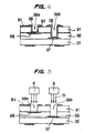
- the printed wiring board is formed by laminating plural insulating layers 91 ⁇ 93 one upon the other and electrically connecting innerlayer conductor circuits 95, 97 arranged between the layers to an outer conductor circuit 94 existing on an outermost surface through metal plated films 96 formed on via-holes 99a, 99b as shown, for example, in Fig. 4 .
- the insulating layers 91 ⁇ 93 is used a resin substrate such as glass-epoxy substrate or the like.
- the via-holes 99a, 99b are blind via-holes.each covered at its one end and opened at the other end.
- a method of forming the via-hole there are a method using a drill, a method using a laser beam and the like.
- the above drilling method causes unevenness in the depth accuracy. And also, it is recently demanded to make more fine a diameter of the via-hole with the advance of high densification in a wiring pattern.
- the via-holes 99a, 99b can be formed in a region ranging from an outermost surface of a multilayer laminated plate up to innerlayer conductor circuits existing therein by utilizing a property that laser beams 81. reflect on the innerlayer conductor circuits 95, 97 each made of a metal such as copper foil, metal plated film or the like.
- the reason why the damage is caused in the innerlayer conductor circuit 95 as mentioned above is due to the fact that laser beams 81 having an intensity required for the formation of the deep via-hole 99b are irradiated to not only the shallow via-hole 99a but also the deep via-hole 99b as shown in Fig. 5 .
- the number of via-holes formed in one printed wiring board is as many as, for example, 500 ⁇ 10000, so that it is complicated to adjust the intensity of the laser beam every via-hole and also it is required to use an expensive control device for such an adjustment.
- a black oxide film is formed on the surfaces of the innerlayer conductor circuits 95, 97 for ensuring an adhesion property to the insulating layers 91, 92. Since the black oxide film is high in the energy absorption of laser beam, there is a fear of causing damages such as breakage and the like due to fusion and swelling of the innerlayer conductor circuit provided on its surface with the black oxide film.
- the insulating layer made of the resin or the like is exposed in the via-hole, so that it is difficult to form the metal plated film.
- the joining property between he inner wall of the via-hole and the metal plated film is low and the peeling, dropping-out and the like of the metal plated film are caused, which have a fear of badly affecting the electric conduction of the via-hole.
- the formation of the metal plated film on the via-hole is carried out by flowing an electric plating solution into the via-hole, but as the inner diameter of the hole becomes small, the flowing of the electric plating solution is difficult to make the formation of the plated film ununiform, so that there is caused a fear that the electric conduction of the via-hole is insufficient.
- the invention is to provide a printed wiring board and a method of manufacturing the same which can form via-holes having a reliable electric conduction without causing damages of innerlayer conductor circuits through a laser beam and realize novel circuit formation through the laser beam.
- JP 03211791 discloses a metal board layer structure of printed board which comprises a ring-like dummy land whose outer periphery is smaller than a clearance hole which is formed at the central position of the clearance hole.
- US 4,642,160 teaches a circuit board that is manufactured from a core layer having a conductor run layer overlying the core layer and a continuous layer of dielectric material, by forming a continuous outer layer of conductive material over the layer of dielectric material.
- US 4,258,468 discloses a via formed in a multilayer printed circuit board by etching apertures in annular lands and then directing a beam of laser energy through the aperture.
- EP-A-0180183 teaches a multilayer printing wiring board comprising at least one layer with interlayer connection pattern at the basic grids.
- the present invention provides a printed wiring board comprising two or more insulating layers on an innerlayer conductor circuit, a via-hole extending from an outermost surface of the insulating layer through the two or more insulating layers to the innerlayer conductor circuit and an inner metal plated film formed in the via-hole so as to electrically connect the innerlayer conductor circuit to an outer conductor circuit arranged on the outermost surface, wherein an annular dummy land for reinforcement having an opening hole around the via-hole is arranged in a boundary portion facing the two or more insulating layers to each other and is joined to the inner metal plated film and the annular dummy land has an outer diameter larger than the diameter of the via-hole and characterised in that the opening hole has a diameter equal to the diameter of the via-hole.
- an innerlayer conductor circuit may be arranged in the boundary portion, but the annular dummy land is separately arranged so as not to connect to such an innerlayer conductor circuit and is a reinforcing land.
- the annular dummy land is favorable to be made of a metal such as copper nickel or the like.
- the annular reinforcing dummy land is arranged around the via-hole and is joined to the inner metal plated film in the via-hole.
- the inner metal plated film hardly joins to an exposed portion of the insulating layer in the via-hole, but strongly joins to the side face of the annular dummy land. Therefore, the inner metal plated film is strongly joined to the inside of the via-hole.
- the innerlayer conductor circuit may be arranged in the boundary portion, but when the via-hole is formed in a portion having no innerlayer conductor circuit, an opening peripheral edge of the via-hole becomes thin by a thickness of the innerlayer conductor circuit as compared with a place having the innerlayer conductor circuit in the boundary portion.
- a depression corresponding to the thickness of the innerlayer conductor circuit is formed in the opening peripheral edge of the via-hole. This is particularly liable to be caused in the via-hole formed by passing through four or more insulating layers (see Fig. 3 ).
- the occurrence of the depression in the opening peripheral edge of the via-hole can be prevented by arranging the annular dummy land.
- the printed wiring board in which the inner metal plated film is strongly joined to the inside of the via-hole.
- the printed wiring board obtained in the invention can be used in, for example, memory module, multi-chip module, mother board, daughter board, plastic package or the like which highly requires the connection reliability.
- the annular dummy land is favorable to have an outer diameter larger than the diameter of the via-hole and include an opening hole having a diameter equal to the diameter of the via-hole.
- the annular dummy land can more stably be arranged and also the reinforcing effect can be more enhanced.
- the present invention further provides a method of manufacturing a printed wiring board comprising two or more insulating layers on an innerlayer conductor circuit, a via-hole extending from an outermost surface of the insulating layers through the two or more insulating layers to the innerlayer conductor circuit and an inner metal plated film formed in the via-hole so as to electrically connect the innerlayer conductor circuit to an outer conductor circuit arranged on the outermost surface, wherein an annular dummy land for reinforcement having an opening hole around the via-hole is arranged in a boundary portion facing the two or more insulating layers to each other and is joined to the inner metal plated film, characterised in that the via-hole is formed by irradiating a laser beam from the outermost surface toward the innerlayer conductor circuit in which the laser beam is arrived to the innerlayer conductor circuit through the opening hole of the annular dummy land and thereafter the inner metal plated film is formed; and in that the annular dummy land has an outer diameter larger than the diameter of the via-hole and includes an opening hole having
- a printed wiring board wherein the inner metal plated film is strongly joined to the inside of the via-hole can be obtained likewise the above printed wiring board.
- via-hole is formed by the irradiation of the laser beam, via-holes having a very fine diameter of not more than 300 ⁇ m can easily be obtained.
- the formation of the via-hole through the laser beam is carried out by irradiating the laser beam to a portion forming the via-hole.
- the laser beam it is favorable to use a carbon dioxide gas laser having a large energy and an excimer laser having no heat affection.
- the insulating layers are vaporized and removed by a high energy to successively form a hole toward the inside of the printed wiring board.
- the laser beam arrives at the innerlayer conductor circuit, it is reflected by the innerlayer conductor circuit made of the metal. Therefore, the irradiation of the laser beam stops at this time.
- the annular dummy land is favorable to have an outer diameter larger than the diameter of the via-hole and include an opening hole having a diameter equal to the diameter of the via-hole.
- the annular dummy land can more stably be arranged and also the reinforcing effect can be more enhanced likewise the above case.
- the annular dummy land is separately arranged so as not to connect to such an innerlayer conductor circuit and is a reinforcing land.
- the annular dummy land is favorable to be made of a metal such as copper nickel or the like.
- the annular reinforcing dummy land is arranged around the via-hole and is joined to the inner metal plated film in the via-hole.
- the inner metal plated film hardly joins to an exposed portion of the insulating layer in the via-hole, but strongly joins to the side face of the annular dummy land. Therefore, the inner metal plated film is strongly joined to the inside of the via-hole.
- the innerlayer conductor circuit may be arranged in the boundary portion, but when the via-hole is formed in a portion having no innerlayer conductor circuit, an opening peripheral edge of the via-hole becomes thin by a thickness of the innerlayer conductor circuit as compared with a place having the innerlayer conductor circuit in the boundary portion.
- a depression corresponding to the thickness of the innerlayer conductor circuit is formed in the opening peripheral edge of the via-hole. This is particularly liable to be caused in the via-hole formed by passing through four or more insulating layers (see Fig. 3 ).
- the occurrence of the depression in the opening peripheral edge of the via-hole can be prevented by arranging the annular dummy land.
- the printed wiring board in which the inner metal plated film is strongly joined to the inside of the via-hole.
- the printed wiring board obtained in the invention can be used in, for example, memory module, multi-chip module, mother board, daughter board, plastic package or the like which highly requires the connection reliability.
- the annular dummy land is favorable to have an outer diameter larger than the diameter of the via-hole and include an opening hole having a diameter equal to the diameter of the via-hole.
- the annular dummy land can more stably be arranged and also the reinforcing effect can be more enhanced.
- a method of manufacturing a printed wiring board comprising two or more insulating layers on an innerlayer conductor circuit, a via-hole extending from an outermost surface of the insulating layer through the two or more insulating layers to the innerlayer conductor circuit and an inner metal plated film formed in the via-hole so as to electrically connect the innerlayer conductor circuit to an outer conductor circuit arranged on the outermost surface, wherein an annular dummy land for reinforcement having an opening hole around the via-hole is arranged in a boundary portion facing the two or more insulating layers to each other and is joined to the inner metal plated film, characterized in that the via-hole is formed by irradiating a laser beam from the outermost surface toward the innerlayer conductor circuit in which the laser beam is arrived to the innerlayer conductor circuit through the opening hole of the annular dummy land, and thereafter the inner metal plated film is formed.
- a printed wiring board wherein the inner metal plated film is strongly joined to the inside of the via-hole can be obtained likewise the above printed wiring board.
- via-hole is formed by the irradiation of the laser beam, via-holes having a very fine diameter of not more than 300 ⁇ m can easily be obtained.
- the formation of the via-hole through the laser beam is carried out by irradiating the laser beam to a portion forming the via-hole.
- the laser beam it is favorable to use a carbon dioxide gas laser having a large energy and an excimer laser having no heat affection.
- the insulating layers are vaporized and removed by a high energy to successively form a hole toward the inside of the printed wiring board.
- the laser beam arrives at the innerlayer conductor circuit, it is reflected by the innerlayer conductor circuit made of the metal. Therefore, the irradiation of the laser beam stops at this time.
- the annular dummy land is favorable to have an outer diameter larger than the diameter of the via-hole and include an opening hole having a diameter equal to the diameter of the via-hole.
- the annular dummy land can more stably be arranged and also the reinforcing effect can be more enhanced likewise the above case.
- film is strongly joined to the inside of the via-hole.
- the printed wiring board obtained in the invention can be used in, for example, memory module, multi-chip module, mother board, daughter board, plastic package or the like which highly requires the connection reliability.
- the annular dummy land is favorable to have an outer diameter larger than the diameter of the via-hole and include an opening hole having a diameter equal to the diameter of the via-hole.
- the annular dummy land can more stably be arranged and also the reinforcing effect can be more enhanced.
- a method of manufacturing a printed wiring board comprising two or more insulating layers on an innerlayer conductor circuit, a via-hole extending from an outermost surface of the insulating layer through the two or more insulating layers to the innerlayer conductor circuit and an inner metal plated film formed in the via-hole so as to electrically connect the innerlayer conductor circuit to an outer conductor circuit arranged on the outermost surface, wherein an annular dummy land for reinforcement having an opening hole around the via-hole is arranged in a boundary portion facing the two or more insulating layers to each other and is joined to the inner metal plated film, characterized in that the via-hole is formed by irradiating a laser beam from the outermost surface toward the innerlayer conductor circuit in which the laser beam is arrived to the innerlayer conductor circuit through the opening hole of the annular dummy land, and thereafter the inner metal plated film is formed.
- a printed wiring board wherein the inner metal plated film is strongly joined to the inside of the via-hole can be obtained likewise the above printed wiring board.
- via-hole is formed by the irradiation of the laser beam, via-holes having a very fine diameter of not more than 300 ⁇ m can easily be obtained.
- the formation of the via-hole through the laser beam is carried out by irradiating the laser beam to a portion forming the via-hole.
- the laser beam it is favorable to use a carbon dioxide gas laser having a large energy and an excimer laser having no heat affection.
- the insulating layers are vaporized and removed by a high energy to successively form a hole toward the inside of the printed wiring board.
- the laser beam arrives at the innerlayer conductor circuit, it is reflected by the innerlayer conductor circuit made of the metal. Therefore, the irradiation of the laser beam stops at this time.
- the annular dummy land is favorable to have an outer diameter larger than the diameter of the via-hole and include an opening hole having a diameter equal to the diameter of the via-hole.
- the annular dummy land can more stably be arranged and also the reinforcing effect can be more enhanced likewise the above case.
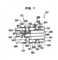
- a printed wiring board according to the invention is described with reference to Figs. 1 and 2 .
- insulating layers 518,516 are laminated onto each face of an innerlayer conductor circuit 562, and a via-hole 502 extending from an outermost surface of the insulating layer 516 through the two insulating layers 518, 516 to the innerlayer conductor circuit 562 is formed.
- the via-hole 502 is formed an inner metal plated film 521 electrically connecting the innerlayer conductor circuit 562 to an outerlayer conductor circuit 561.
- the via-hole 502 is a blind via-hole.
- a reinforcing annular dummy land 504 having an opening hole 540 around the via-hole 502 is formed in a boundary portion 517 between the two insulating layers 518, 516 as shown in Fig. 2 .
- the annular dummy land 504 is adhered to the inner metal plated film 521.
- the printed wiring board 501 comprises an innerlayer plate 519 provided with an innerlayer conductor circuit 562, two insulating layers 518, 516 laminated on each surface of the innerlayer plate 519, innerlayer conductor circuits 563 and annular dummy land 504 arranged on the surface of the insulating layer 518 and outerlayer conductor circuits 561 arranged on the surface of the insulating layer 516.
- a through-hole 528 is formed in the innerlayer plate 519.
- a metal plated film 505 electrically connecting the two innerlayer conductor circuits 562 formed on both surfaces of the innerlayer plate 519 to each other.
- a via-hole 502 extending from an outermost surface of the insulating layer 516 to the innerlayer conductor circuit 562 and a via-hole 529 extending from the outermost surface of the insulating layer 516 to the innerlayer conductor circuit 563.
- the via-hole 502 is formed in a portion existing no innerlayer conductor circuit 563.
- an opening hole 540 of the annular dummy land 504 is exposed between the insulating layers 518, 516.
- the inner metal plated film 521 is adhered to the inner wall face 520 of the via-hole 502, but is a state of adhering to an outerlayer conductor circuit 561 mainly existing on an opening peripheral edge 525 of the via-hole 502, the opening hole 540 of the annular dummy land 504 and an innerlayer conductor circuit 562 facing the bottom of the via-hole 502.
- the annular dummy land 504 is made of a copper plated layer, and has an outer diameter larger than the diameter of the via-hole 502 and an opening hole 540 having the same diameter as the via-hole 502 as shown in Fig. 2 . And also, the annular dummy land 504 is formed by etching in the formation of the innerlayer conductor circuit 563.
- annular dummy land 504 is a reinforcing land separately arranged so as not to electrically connect to the innerlayer conductor circuit 563.
- a via-hole 529 is formed so as to extend through the insulating layer 516 to the innerlayer conductor circuit 563.
- An inner metal plated film 521 is also formed in the via-hole 529.
- the inner metal plate film 521 is a state of adhering to the innerlayer conductor circuit 561 mainly arranged on an opening peripheral edge 25 of the via-hole 529, an inner wall of the via-hole 529 and an innerlayer conductor circuit 516 facing the bottom of the via-hole 529.
- a prepreg and a copper foil are laminated on the surface of the innerlayer plate 519. Thereafter, the copper foil is patterned by etching to form an insulating layer 518 having an innerlayer conductor circuit 563 and an annular dummy land 504.
- a laser beam is irradiated from the outermost surface of the insulating layer 516.
- the laser beam is arrived at the innerlayer conductor circuit 562 through the opening hole 540 of the annular dummy land 504.
- inner metal plated films 505 are formed in the via-holes 502, 529 by electroless copper plating.
- the via-holes 502, 529 have a diameter of 100 ⁇ m
- the annular dummy land 504 is provided with the opening hole 540 having a diameter of 100 ⁇ m and has an outer diameter of 200 ⁇ m.
- an excimer laser is used at a wavelength of 248 nm and an output of 50 W as the laser beam.
- the annular dummy land 504 is formed around the via-hole 502, and such an annular dummy land 504 is adhered to the innerlayer conductor circuit 521 in the via-hole 502.
- the inner metal plated film 521 hardly adheres to exposed portions of the insulating layers 518, 516 in the via-hole 502 and is weak in the adhesion strength, but can strongly adhere to the annular dummy land 504.
- the inner metal plated film 521 can strongly be adhered to he via-hole 502. As a result, there can be prevented the separation and falling down of the inner metal plated film 521.
- the via-holes 502, 529 in the printed wiring board 501 of this embodiment are formed by the irradiation of the laser beam, so that the size can be more fined.
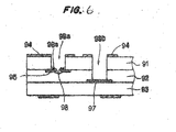
- a printed wiring board 508 in which a via-hole 503 passes through five insulating layers 511-515 as shown in Figure 3 .
- the printed wiring board 508 is a laminate comprised of an innerlayer plate 519 and five insulating layers 511 ⁇ 515. On the surfaces of the innerlayer plate 519 are formed an innerlayer conductor circuit 562 and an outerlayer conductor circuit 561. On the insulating layer 519 is formed an outerlayer conductor circuit 561.
- innerlayer conductor circuits 563, 564 are formed on boundary portions 517 among these insulating layers 511 ⁇ 515.
- the inner-layer conductor circuit 563 is not conductive to the via-hole 503, while the other innerlayer conductor circuit 56 is conductive to the via-hole 503.
- the via-hole 503 is formed so as to pass through the innerlayer conductor circuit 564.
- the via-hole 503 is formed in portions of the insulating layers 511, 512, 514 including no innerlayer conductor circuit 563 and provided with reinforcing annular dummy lands 504 having an opening hole 540.
- an inner metal plated film 521 formed in the via-hole 503 adheres to an inner wall face 530 of the via-hole 503, but is a state of adhering to an outerlayer conductor circuit 561 mainly existing on an opening peripheral edge 535 of the via-hole 503, the opening hole 540 of the annular dummy land 504 and an innerlayer conductor circuit 562 facing the bottom of the via-hole 503.
- the innerlayer conductor circuits 563, 187 are formed on boundary portions 517 among the different insulating layers 511 ⁇ 515. And also, the via-hole 503 is formed in a portion including no innerlayer conductor circuit 563 but including the innerlayer conductor circuit 564.
- the opening peripheral edge 535 of the via-hole 503 is decreased by a total thickness of the innerlayer conductor circuits 563 formed on the insulating layers 511, 512, 514.
- the annular dummy land 504 is formed in the printed wiring board 508 of this embodiment, so that the metal plated film 521 is strongly adhered thereto and there is caused depression or the like in the opening peripheral edge 535 of the via-hole 503.
- via-holes having a sure conductivity can be formed through the laser beam without causing damage of innerlayer conductor circuit and there can be provided a production method of a printed wiring board capable of realizing novel circuit formation through the laser beam.
Landscapes
- Engineering & Computer Science (AREA)
- Microelectronics & Electronic Packaging (AREA)
- Manufacturing & Machinery (AREA)
- Physics & Mathematics (AREA)
- Optics & Photonics (AREA)
- Production Of Multi-Layered Print Wiring Board (AREA)
- Laser Beam Processing (AREA)
- Structure Of Printed Boards (AREA)
- Printing Elements For Providing Electric Connections Between Printed Circuits (AREA)
Claims (2)
- Leiterplatte (501), die zwei oder mehr Isolierschichten (516, 518) auf einer Innenschichtleiterschaltung (562), ein Durchgangsloch (502), das sich von einer äußersten Oberfläche der Isolierschicht (516) durch die zwei oder mehr Isolierschichten (516, 518) zu der Innenschichtleiterschaltung (562) erstreckt, und einen inneren, mit Metall überzogenen Film (505) aufweist, der in dem Durchgangsloch (502) ausgeformt ist, um die Innenschichtleiterschaltung (562) elektrisch mit einer äußeren, auf der äußersten Oberfläche angeordneten Leiterschaltung zu verbinden, wobei eine ringförmige Dummy-Fläche (504) zur Verstärkung, die ein Öffnungsloch um das Durchgangsloch (502) aufweist, in einem Randbereich angeordnet ist, der den zwei oder mehr Isolierschichten (516, 518) zugewandt liegend angeordnet ist, und mit dem inneren, mit Metall überzogenen Film (505) verbunden ist, und die ringförmige Dummy-Fläche (504) einen äußeren Durchmesser aufweist, der größer ist als der Durchmesser des Durchgangslochs (502), und dadurch gekennzeichnet, dass das Öffnungsloch der ringförmigen Dummy-Fläche einen Durchmesser gleich dem Durchmesser des Durchgangslochs (502) aufweist.
- Verfahren zur Herstellung einer Leiterplatte (501), die zwei oder mehr Isolierschichten (516, 518) auf einer Innenschichtleiterschaltung (562), ein Durchgangsloch (502), das sich von einer äußersten Oberfläche der Isolierschicht (516) durch die zwei oder mehr Isolierschichten (516, 518) zu der Innenschichtleiterschaltung (562) erstreckt, und einen inneren, mit Metall überzogenen Film (505) aufweist, der in dem Durchgangsloch (502) ausgeformt ist, um so die Innenschichtleiterschaltung (562) elektrisch mit einer äußeren, auf der äußersten Oberfläche angeordneten Leiterschaltung zu verbinden, wobei eine ringförmige Dummy-Fläche (504) zur Verstärkung, die ein Öffnungsloch um das Durchgangsloch (502) aufweist, in einem Randbereich angeordnet ist, der den zwei oder mehr Isolierschichten (516, 518) zugewandt angeordnet ist, und mit dem inneren, mit Metall überzogenen Film (505) verbunden ist, dadurch gekennzeichnet, dass das Durchgangsloch (502) durch Bestrahlen mit einem Laserstrahl von der äußersten Oberfläche in Richtung der Innenschichtleiterschaltung (562) ausgeformt wird, wobei der Laserstrahl durch das Öffnungsloch der ringförmigen Dummy-Fläche (504) bei der Innenschichtleiterschaltung (562) eintrifft, und danach der innere, mit Metall überzogene Film (505) ausgeformt wird; und dadurch, dass die ringförmige Dummy-Fläche (504) einen äußeren Durchmesser aufweist, der größer ist als der Durchmesser des Durchgangslochs (502), und ein Öffnungsloch aufweist, das einen Durchmesser gleich dem Durchmesser des Durchgangslochs (502) aufweist.
Applications Claiming Priority (12)
| Application Number | Priority Date | Filing Date | Title |
|---|---|---|---|
| JP3563397 | 1997-02-03 | ||
| JP4724897 | 1997-02-13 | ||
| JP4988397 | 1997-02-17 | ||
| JP5248297 | 1997-02-19 | ||
| JP5248497 | 1997-02-19 | ||
| JP5248397 | 1997-02-19 | ||
| JP6192197 | 1997-02-27 | ||
| JP6551197 | 1997-03-03 | ||
| JP6915897 | 1997-03-05 | ||
| JP8578697 | 1997-03-19 | ||
| JP36726897A JP3395621B2 (ja) | 1997-02-03 | 1997-12-24 | プリント配線板及びその製造方法 |
| EP98901002A EP0971570B1 (de) | 1997-02-03 | 1998-01-23 | Gedruckte leiterplatte und verfahren zu deren herstellung |
Related Parent Applications (2)
| Application Number | Title | Priority Date | Filing Date |
|---|---|---|---|
| EP98901002A Division EP0971570B1 (de) | 1997-02-03 | 1998-01-23 | Gedruckte leiterplatte und verfahren zu deren herstellung |
| EP98901002.0 Division | 1998-08-06 |
Publications (3)
| Publication Number | Publication Date |
|---|---|
| EP1816905A2 EP1816905A2 (de) | 2007-08-08 |
| EP1816905A3 EP1816905A3 (de) | 2007-10-03 |
| EP1816905B1 true EP1816905B1 (de) | 2010-10-06 |
Family
ID=27581955
Family Applications (5)
| Application Number | Title | Priority Date | Filing Date |
|---|---|---|---|
| EP07075315A Expired - Lifetime EP1827069B1 (de) | 1997-02-03 | 1998-01-23 | Leiterplatte und Herstellungsverfahren dafür |
| EP07075317A Withdrawn EP1827068A3 (de) | 1997-02-03 | 1998-01-23 | Leiterplatte und Herstellungsverfahren dafür |
| EP07075316A Expired - Lifetime EP1816905B1 (de) | 1997-02-03 | 1998-01-23 | Leiterplatte und Herstellungsverfahren dafür |
| EP07075318A Withdrawn EP1827065A3 (de) | 1997-02-03 | 1998-01-23 | Leiterplatte und Herstellungsverfahren dafür |
| EP98901002A Expired - Lifetime EP0971570B1 (de) | 1997-02-03 | 1998-01-23 | Gedruckte leiterplatte und verfahren zu deren herstellung |
Family Applications Before (2)
| Application Number | Title | Priority Date | Filing Date |
|---|---|---|---|
| EP07075315A Expired - Lifetime EP1827069B1 (de) | 1997-02-03 | 1998-01-23 | Leiterplatte und Herstellungsverfahren dafür |
| EP07075317A Withdrawn EP1827068A3 (de) | 1997-02-03 | 1998-01-23 | Leiterplatte und Herstellungsverfahren dafür |
Family Applications After (2)
| Application Number | Title | Priority Date | Filing Date |
|---|---|---|---|
| EP07075318A Withdrawn EP1827065A3 (de) | 1997-02-03 | 1998-01-23 | Leiterplatte und Herstellungsverfahren dafür |
| EP98901002A Expired - Lifetime EP0971570B1 (de) | 1997-02-03 | 1998-01-23 | Gedruckte leiterplatte und verfahren zu deren herstellung |
Country Status (6)
| Country | Link |
|---|---|
| US (2) | US6590165B1 (de) |
| EP (5) | EP1827069B1 (de) |
| JP (1) | JP3395621B2 (de) |
| KR (1) | KR100325372B1 (de) |
| AT (1) | ATE368370T1 (de) |
| WO (1) | WO1998034447A1 (de) |
Families Citing this family (106)
| Publication number | Priority date | Publication date | Assignee | Title |
|---|---|---|---|---|
| US6707152B1 (en) | 1999-04-16 | 2004-03-16 | Micron Technology, Inc. | Semiconductor device, electrical conductor system, and method of making |
| JP2001007526A (ja) * | 1999-06-18 | 2001-01-12 | Ibiden Co Ltd | 多層ビルドアップ配線板及び多層ビルドアップ配線板の製造方法 |
| DE60042976D1 (de) | 1999-08-06 | 2009-10-29 | Ibiden Co Ltd | Lösung für die elektrochemische abscheidung, methode, eine leiterplatte unter verwendung dieser lösung herzustellen und mehrschichtige leiterplatte |
| JP2001308530A (ja) * | 2000-04-24 | 2001-11-02 | Ibiden Co Ltd | 積層配線板およびその製造方法 |
| JP2002319762A (ja) * | 2001-04-20 | 2002-10-31 | Toppan Printing Co Ltd | 多層配線基板 |
| JP4079699B2 (ja) * | 2001-09-28 | 2008-04-23 | 富士通株式会社 | 多層配線回路基板 |
| JP3728495B2 (ja) * | 2001-10-05 | 2005-12-21 | 独立行政法人産業技術総合研究所 | 多層膜マスク欠陥検査方法及び装置 |
| JP2003133366A (ja) * | 2001-10-25 | 2003-05-09 | Texas Instr Japan Ltd | 半導体装置及びその製造方法 |
| JP2003136268A (ja) * | 2001-11-06 | 2003-05-14 | Hitachi Via Mechanics Ltd | プリント基板の穴あけ加工方法 |
| US7138733B2 (en) * | 2001-12-13 | 2006-11-21 | Hewlett-Packard Development Company, L.P. | Redundant data and power infrastructure for modular server components in a rack |
| US9691635B1 (en) | 2002-05-01 | 2017-06-27 | Amkor Technology, Inc. | Buildup dielectric layer having metallization pattern semiconductor package fabrication method |
| US7548430B1 (en) | 2002-05-01 | 2009-06-16 | Amkor Technology, Inc. | Buildup dielectric and metallization process and semiconductor package |
| US7084354B2 (en) * | 2002-06-14 | 2006-08-01 | Intel Corporation | PCB method and apparatus for producing landless interconnects |
| JP2003163465A (ja) * | 2002-11-19 | 2003-06-06 | Ibiden Co Ltd | プリント配線板の製造方法 |
| US20040219342A1 (en) * | 2003-01-07 | 2004-11-04 | Boggs David W. | Electronic substrate with direct inner layer component interconnection |
| JP4054269B2 (ja) * | 2003-03-20 | 2008-02-27 | Tdk株式会社 | 電子部品の製造方法および電子部品 |
| KR100629887B1 (ko) * | 2003-05-14 | 2006-09-28 | 이규한 | 금속 칩스케일 반도체패키지 및 그 제조방법 |
| US7071419B2 (en) * | 2003-10-08 | 2006-07-04 | Motorola, Inc. | Tear resistant flexible substrate |
| JP4401912B2 (ja) * | 2003-10-17 | 2010-01-20 | 学校法人早稲田大学 | 半導体多層配線板の形成方法 |
| US7211289B2 (en) * | 2003-12-18 | 2007-05-01 | Endicott Interconnect Technologies, Inc. | Method of making multilayered printed circuit board with filled conductive holes |
| US11081370B2 (en) | 2004-03-23 | 2021-08-03 | Amkor Technology Singapore Holding Pte. Ltd. | Methods of manufacturing an encapsulated semiconductor device |
| US10811277B2 (en) | 2004-03-23 | 2020-10-20 | Amkor Technology, Inc. | Encapsulated semiconductor package |
| US7852635B1 (en) * | 2004-05-25 | 2010-12-14 | Lineage Power Corporation | Multi-connection via |
| US7317255B2 (en) * | 2004-09-30 | 2008-01-08 | Kyocera Wireless Corp. | Reliable printed wiring board assembly employing packages with solder joints |
| JP2006100631A (ja) * | 2004-09-30 | 2006-04-13 | Tdk Corp | 配線基板及びその製造方法 |
| JP4608297B2 (ja) | 2004-12-06 | 2011-01-12 | インターナショナル・ビジネス・マシーンズ・コーポレーション | 積層配線基板の製造方法 |
| JP4584700B2 (ja) * | 2004-12-17 | 2010-11-24 | 新光電気工業株式会社 | 配線基板の製造方法 |
| JP2006179822A (ja) * | 2004-12-24 | 2006-07-06 | Cmk Corp | プリント配線板とその製造方法 |
| JP2006245076A (ja) * | 2005-03-01 | 2006-09-14 | Matsushita Electric Ind Co Ltd | 半導体装置 |
| US7838779B2 (en) * | 2005-06-17 | 2010-11-23 | Nec Corporation | Wiring board, method for manufacturing same, and semiconductor package |
| TWI283152B (en) * | 2005-06-20 | 2007-06-21 | Phoenix Prec Technology Corp | Structure of circuit board and method for fabricating the same |
| US7649375B2 (en) * | 2005-06-30 | 2010-01-19 | Teradyne, Inc. | Connector-to-pad printed circuit board translator and method of fabrication |
| JP2007027476A (ja) * | 2005-07-19 | 2007-02-01 | Sharp Corp | 多層プリント配線板の製造方法および多層プリント配線板 |
| JP5025113B2 (ja) * | 2005-09-29 | 2012-09-12 | 三洋電機株式会社 | 回路装置 |
| TW200746940A (en) * | 2005-10-14 | 2007-12-16 | Ibiden Co Ltd | Printed wiring board |
| JP4899409B2 (ja) * | 2005-10-21 | 2012-03-21 | パナソニック株式会社 | 多層プリント配線基板及びその製造方法 |
| JP5016876B2 (ja) * | 2006-09-06 | 2012-09-05 | 株式会社ディスコ | ビアホールの加工方法 |
| US7557304B2 (en) * | 2006-11-08 | 2009-07-07 | Motorola, Inc. | Printed circuit board having closed vias |
| JP5409996B2 (ja) | 2006-12-25 | 2014-02-05 | ピーエスフォー ルクスコ エスエイアールエル | 多層プリント配線板 |
| JP2008182163A (ja) * | 2007-01-26 | 2008-08-07 | Shinko Electric Ind Co Ltd | 配線基板及びその製造方法と半導体装置 |
| US7829462B2 (en) * | 2007-05-03 | 2010-11-09 | Teledyne Licensing, Llc | Through-wafer vias |
| US8440916B2 (en) * | 2007-06-28 | 2013-05-14 | Intel Corporation | Method of forming a substrate core structure using microvia laser drilling and conductive layer pre-patterning and substrate core structure formed according to the method |
| US8877565B2 (en) * | 2007-06-28 | 2014-11-04 | Intel Corporation | Method of forming a multilayer substrate core structure using sequential microvia laser drilling and substrate core structure formed according to the method |
| JP5094323B2 (ja) | 2007-10-15 | 2012-12-12 | 新光電気工業株式会社 | 配線基板の製造方法 |
| KR101164598B1 (ko) * | 2007-10-16 | 2012-07-10 | 삼성테크윈 주식회사 | 다층 회로기판의 제조 방법 |
| JP4309448B2 (ja) | 2007-11-27 | 2009-08-05 | 株式会社東芝 | 多層プリント配線板、ビルドアッププリント配線板の製造方法および電子機器 |
| JP2009206506A (ja) * | 2008-01-31 | 2009-09-10 | Sanyo Electric Co Ltd | 素子搭載用基板およびその製造方法、半導体モジュールおよびこれを搭載した携帯機器 |
| JP5284146B2 (ja) * | 2008-03-13 | 2013-09-11 | 日本特殊陶業株式会社 | 多層配線基板、及びその製造方法 |
| US7932170B1 (en) * | 2008-06-23 | 2011-04-26 | Amkor Technology, Inc. | Flip chip bump structure and fabrication method |
| EP2244285A1 (de) * | 2009-04-24 | 2010-10-27 | ATOTECH Deutschland GmbH | Verfahren zur Formung von Lötablagerungen auf Substraten |
| WO2010046235A1 (en) * | 2008-10-21 | 2010-04-29 | Atotech Deutschland Gmbh | Method to form solder deposits on substrates |
| KR101006603B1 (ko) * | 2009-01-09 | 2011-01-07 | 삼성전기주식회사 | 인쇄회로기판 및 그 제조방법 |
| DE102009029114B4 (de) * | 2009-09-02 | 2017-06-01 | Robert Bosch Gmbh | Mikromechanisches System |
| KR101051551B1 (ko) * | 2009-10-30 | 2011-07-22 | 삼성전기주식회사 | 요철 패턴을 갖는 비아 패드를 포함하는 인쇄회로기판 및 그 제조방법 |
| US8365399B2 (en) * | 2009-12-03 | 2013-02-05 | International Business Machines Corporation | Method of connecting components to a printed circuit board |
| US8207453B2 (en) | 2009-12-17 | 2012-06-26 | Intel Corporation | Glass core substrate for integrated circuit devices and methods of making the same |
| TWI393508B (zh) * | 2009-12-17 | 2013-04-11 | Unimicron Technology Corp | 線路板及其製程 |
| US9420707B2 (en) * | 2009-12-17 | 2016-08-16 | Intel Corporation | Substrate for integrated circuit devices including multi-layer glass core and methods of making the same |
| JP5360494B2 (ja) * | 2009-12-24 | 2013-12-04 | 新光電気工業株式会社 | 多層配線基板、多層配線基板の製造方法、及びヴィアフィル方法 |
| TWI399143B (zh) * | 2009-12-30 | 2013-06-11 | Unimicron Technology Corp | 線路板及其製程 |
| US10297550B2 (en) | 2010-02-05 | 2019-05-21 | Taiwan Semiconductor Manufacturing Company, Ltd. | 3D IC architecture with interposer and interconnect structure for bonding dies |
| JP5450272B2 (ja) * | 2010-06-10 | 2014-03-26 | 日本メクトロン株式会社 | レーザ加工方法、及び該レーザ加工方法を用いた多層フレキシブルプリント配線板の製造方法 |
| KR20120017245A (ko) * | 2010-08-18 | 2012-02-28 | 삼성전기주식회사 | 인쇄회로기판 및 이의 제조방법 |
| US8756803B2 (en) * | 2010-09-22 | 2014-06-24 | Ibiden Co., Ltd. | Method for manufacturing printed wiring board |
| JP5602584B2 (ja) * | 2010-10-28 | 2014-10-08 | 新光電気工業株式会社 | 配線基板及びその製造方法 |
| CN102006721B (zh) * | 2010-11-19 | 2015-10-21 | 中兴通讯股份有限公司 | 印刷电路板基板及其制作方法 |
| JP5170227B2 (ja) * | 2010-12-10 | 2013-03-27 | 富士通セミコンダクター株式会社 | 多層配線基板及びその製造方法 |
| US8595927B2 (en) * | 2011-03-17 | 2013-12-03 | Ibiden Co., Ltd. | Method for manufacturing multilayer printed wiring board |
| WO2013133827A1 (en) | 2012-03-07 | 2013-09-12 | Intel Corporation | Glass clad microelectronic substrate |
| US9860985B1 (en) | 2012-12-17 | 2018-01-02 | Lockheed Martin Corporation | System and method for improving isolation in high-density laminated printed circuit boards |
| US9337613B1 (en) * | 2013-03-12 | 2016-05-10 | Western Digital Technologies, Inc. | Chip on submount carrier fixture |
| US20140268610A1 (en) * | 2013-03-15 | 2014-09-18 | Gregory HALVORSON | Method and system for forming a microvia in a printed circuit board |
| JP6273684B2 (ja) * | 2013-03-18 | 2018-02-07 | 富士通株式会社 | 電子機器の外装部材、電子機器、電子機器の外装部材の製造方法 |
| JP2014220330A (ja) * | 2013-05-07 | 2014-11-20 | 日立金属株式会社 | 光配線基板、光配線基板の製造方法、及び光モジュール |
| US20150014044A1 (en) * | 2013-07-15 | 2015-01-15 | International Business Machines Corporation | High speed via |
| KR101483874B1 (ko) * | 2013-07-29 | 2015-01-16 | 삼성전기주식회사 | 인쇄회로기판 |
| CN104955276A (zh) * | 2014-03-24 | 2015-09-30 | 深南电路有限公司 | 电路板台阶孔的加工方法和具有台阶孔的电路板 |
| TWI667865B (zh) * | 2014-05-07 | 2019-08-01 | 易鼎股份有限公司 | Flexible circuit board line lap structure |
| KR102211741B1 (ko) * | 2014-07-21 | 2021-02-03 | 삼성전기주식회사 | 인쇄회로기판 및 인쇄회로기판의 제조 방법 |
| JP6329027B2 (ja) * | 2014-08-04 | 2018-05-23 | ミネベアミツミ株式会社 | フレキシブルプリント基板 |
| RU2572831C1 (ru) * | 2014-09-03 | 2016-01-20 | Открытое акционерное общество "Научно-производственное предприятие "Полет" | Способ изготовления печатных плат |
| US20160074968A1 (en) * | 2014-09-11 | 2016-03-17 | Suss Microtec Photonic Systems Inc. | Laser etching system including mask reticle for multi-depth etching |
| CN107404804B (zh) * | 2016-05-20 | 2020-05-22 | 鹏鼎控股(深圳)股份有限公司 | 电路板及其制作方法 |
| WO2018042846A1 (ja) * | 2016-08-30 | 2018-03-08 | 株式会社村田製作所 | 電子デバイス及び多層セラミック基板 |
| US10251270B2 (en) * | 2016-09-15 | 2019-04-02 | Innovium, Inc. | Dual-drill printed circuit board via |
| CN108156748A (zh) * | 2017-12-29 | 2018-06-12 | 加弘科技咨询(上海)有限公司 | 印制电路板双面贴装时的信号线扇出方法及印制电路板 |
| CN108401358B (zh) * | 2018-01-24 | 2020-06-23 | 广州兴森快捷电路科技有限公司 | 印制电路板及印制电路板的制作方法 |
| DE102018127630A1 (de) * | 2018-11-06 | 2020-05-07 | Bundesdruckerei Gmbh | Durchkontaktierung einer beidseitig bedruckten Trägerfolie mit Fülldruck |
| DE102018127631A1 (de) * | 2018-11-06 | 2020-05-07 | Bundesdruckerei Gmbh | Durchkontaktierung in einer beidseitig bedruckten Trägerfolie mit mehrstufiger Bohrung |
| US12250863B2 (en) | 2019-01-31 | 2025-03-11 | MIANYANG BOE OPTOELECTRONICS TECHNOLOGY CO., Ltd | OLED display panel and OLED display device |
| CN109801874A (zh) * | 2019-01-31 | 2019-05-24 | 绵阳京东方光电科技有限公司 | 过孔结构及其制造方法、电子器件、显示装置 |
| KR102591926B1 (ko) * | 2019-07-31 | 2023-10-19 | 셰난 서키츠 씨오., 엘티디. | 회로 기판 및 그 제작 방법 |
| CN110391515B (zh) * | 2019-08-20 | 2024-03-05 | 广州安博新能源科技有限公司 | 一种具有抗震功能的复合汇流排 |
| US11600519B2 (en) * | 2019-09-16 | 2023-03-07 | International Business Machines Corporation | Skip-via proximity interconnect |
| TWI741370B (zh) * | 2019-09-17 | 2021-10-01 | 李家銘 | 具有層間導孔的線路結構的製法 |
| CN110933856A (zh) * | 2019-12-30 | 2020-03-27 | 东莞市五株电子科技有限公司 | 一种高频盲孔板制作工艺及高频盲孔板 |
| WO2021199336A1 (ja) * | 2020-03-31 | 2021-10-07 | 株式会社メイコー | Ivh多層基板及びその製造方法 |
| US11398419B2 (en) * | 2020-07-16 | 2022-07-26 | Advanced Semiconductor Engineering, Inc. | Wiring structure and method for manufacturing the same |
| TWI740716B (zh) * | 2020-11-16 | 2021-09-21 | 旭德科技股份有限公司 | 基板結構 |
| JP7315523B2 (ja) * | 2020-12-04 | 2023-07-26 | 矢崎総業株式会社 | 端子の固着方法 |
| CN114765923A (zh) * | 2021-05-20 | 2022-07-19 | 上海贺鸿电子科技股份有限公司 | 一种5g基站隔离器三层线路板及其制备方法 |
| JP7485223B2 (ja) * | 2021-07-09 | 2024-05-16 | 住友電気工業株式会社 | プリント配線板 |
| KR102888554B1 (ko) | 2022-01-03 | 2025-11-21 | 삼성전자주식회사 | 반도체 모듈용 모듈 기판, 반도체 모듈 및 이를 테스트하기 위한 테스트 소켓 |
| US20240047229A1 (en) * | 2022-08-02 | 2024-02-08 | Advanced Micro Devices, Inc. | Organic package core for a substrate with high density plated holes |
| CN115799182A (zh) * | 2022-12-02 | 2023-03-14 | 珠海越亚半导体股份有限公司 | 一种元器件封装基板结构及其制作方法 |
| KR102943942B1 (ko) * | 2023-11-27 | 2026-03-27 | 주식회사 웨이브컴퍼니 | 원단의 도전패턴에서의 접합 구조 |
Family Cites Families (39)
| Publication number | Priority date | Publication date | Assignee | Title |
|---|---|---|---|---|
| US3571923A (en) * | 1968-12-30 | 1971-03-23 | North American Rockwell | Method of making redundant circuit board interconnections |
| FR2423953A1 (fr) * | 1978-04-18 | 1979-11-16 | Radiotechnique Compelec | Circuit imprime a composants electroniques incorpores et son procede de fabrication |
| US4258468A (en) * | 1978-12-14 | 1981-03-31 | Western Electric Company, Inc. | Forming vias through multilayer circuit boards |
| JPS5864097A (ja) * | 1981-10-14 | 1983-04-16 | 株式会社日立製作所 | 多層印刷回路板の製造方法 |
| EP0180183A3 (de) * | 1984-10-29 | 1987-09-23 | Kabushiki Kaisha Toshiba | Mehrschichtige gedruckte Schaltungsplatte |
| US4729061A (en) * | 1985-04-29 | 1988-03-01 | Advanced Micro Devices, Inc. | Chip on board package for integrated circuit devices using printed circuit boards and means for conveying the heat to the opposite side of the package from the chip mounting side to permit the heat to dissipate therefrom |
| US4642160A (en) * | 1985-08-12 | 1987-02-10 | Interconnect Technology Inc. | Multilayer circuit board manufacturing |
| JPS62216297A (ja) | 1986-03-17 | 1987-09-22 | 富士通株式会社 | 多層プリント板の孔加工法 |
| US4935584A (en) * | 1988-05-24 | 1990-06-19 | Tektronix, Inc. | Method of fabricating a printed circuit board and the PCB produced |
| US4894115A (en) * | 1989-02-14 | 1990-01-16 | General Electric Company | Laser beam scanning method for forming via holes in polymer materials |
| JPH0734508B2 (ja) * | 1989-04-10 | 1995-04-12 | 三菱電機株式会社 | 多層配線板 |
| JPH0354885A (ja) * | 1989-07-24 | 1991-03-08 | Canon Inc | プリント基板の孔加工方法 |
| JPH03165093A (ja) * | 1989-11-24 | 1991-07-17 | Toshiba Corp | 多層プリント配線板 |
| JPH03165594A (ja) | 1989-11-24 | 1991-07-17 | Ibiden Co Ltd | 多層プリント配線板の製造方法 |
| JPH03211791A (ja) * | 1990-01-12 | 1991-09-17 | Fujitsu Ltd | プリント基板の金属板層構造 |
| JPH045891A (ja) * | 1990-04-23 | 1992-01-09 | Hitachi Seiko Ltd | プリント基板の穴明け加工法 |
| JP2881963B2 (ja) * | 1990-05-25 | 1999-04-12 | ソニー株式会社 | 配線基板及びその製造方法 |
| JPH04233258A (ja) | 1990-07-23 | 1992-08-21 | Internatl Business Mach Corp <Ibm> | 超小型電子回路パッケージ |
| US5191174A (en) * | 1990-08-01 | 1993-03-02 | International Business Machines Corporation | High density circuit board and method of making same |
| JPH04162796A (ja) | 1990-10-26 | 1992-06-08 | Fujitsu Ltd | 薄膜多層基板 |
| JP2539287B2 (ja) * | 1990-11-20 | 1996-10-02 | 日本メクトロン株式会社 | 回路部品搭載用端子を備えた回路基板の製造法 |
| JPH07112113B2 (ja) * | 1991-01-28 | 1995-11-29 | 松下電工株式会社 | 多層回路板のバイアホール加工方法 |
| US5227013A (en) * | 1991-07-25 | 1993-07-13 | Microelectronics And Computer Technology Corporation | Forming via holes in a multilevel substrate in a single step |
| JPH0575253A (ja) * | 1991-08-27 | 1993-03-26 | Hitachi Constr Mach Co Ltd | レーザ光による回路パターンの形成方法及びスルーホール内の導体形成方法 |
| DE4129835A1 (de) * | 1991-09-07 | 1993-03-11 | Bosch Gmbh Robert | Leistungselektroniksubstrat und verfahren zu dessen herstellung |
| JP3002307B2 (ja) * | 1991-10-04 | 2000-01-24 | 日本メクトロン株式会社 | 回路部品試験用可撓性回路基板の製造法 |
| JPH06295962A (ja) * | 1992-10-20 | 1994-10-21 | Ibiden Co Ltd | 電子部品搭載用基板およびその製造方法並びに電子部品搭載装置 |
| JPH06302965A (ja) * | 1993-04-16 | 1994-10-28 | Oki Electric Ind Co Ltd | 薄膜多層基板におけるビア形成方法 |
| CA2143833A1 (en) * | 1993-07-07 | 1995-01-19 | Walter Schmidt | Structured printed circuit boards and foil printed circuit boards and process for the manufacture thereof |
| JP2694802B2 (ja) * | 1993-12-28 | 1997-12-24 | 日本電気株式会社 | プリント配線板の製造方法 |
| JP2611671B2 (ja) * | 1994-07-26 | 1997-05-21 | 日本電気株式会社 | 半導体装置 |
| JPH08330734A (ja) | 1995-05-31 | 1996-12-13 | Mitsubishi Gas Chem Co Inc | ブラインドバイアス孔を有する多層プリント板の製造方法 |
| JPH09130049A (ja) * | 1995-11-01 | 1997-05-16 | Cmk Corp | 多層プリント配線板のビルドアップ法におけるバイア・ホールの形成方法およびそれにより製造される多層プリント配線板 |
| JPH09172261A (ja) * | 1995-12-20 | 1997-06-30 | Nippon Avionics Co Ltd | 多層プリント配線板の製造方法 |
| JP2778569B2 (ja) * | 1996-01-22 | 1998-07-23 | 日立エーアイシー株式会社 | 多層印刷配線板およびその製造方法 |
| US5826330A (en) * | 1995-12-28 | 1998-10-27 | Hitachi Aic Inc. | Method of manufacturing multilayer printed wiring board |
| JPH10190233A (ja) | 1996-12-19 | 1998-07-21 | Victor Co Of Japan Ltd | 多層配線基板の製造方法 |
| JPH10224041A (ja) | 1997-01-31 | 1998-08-21 | Nippon Carbide Ind Co Inc | 多層配線板およびその製造方法 |
| JP3211791B2 (ja) | 1998-12-22 | 2001-09-25 | 日本電気株式会社 | ループ処理方式 |
-
1997
- 1997-12-24 JP JP36726897A patent/JP3395621B2/ja not_active Expired - Fee Related
-
1998
- 1998-01-23 EP EP07075315A patent/EP1827069B1/de not_active Expired - Lifetime
- 1998-01-23 WO PCT/JP1998/000289 patent/WO1998034447A1/ja not_active Ceased
- 1998-01-23 EP EP07075317A patent/EP1827068A3/de not_active Withdrawn
- 1998-01-23 KR KR1019997007007A patent/KR100325372B1/ko not_active Expired - Fee Related
- 1998-01-23 AT AT98901002T patent/ATE368370T1/de not_active IP Right Cessation
- 1998-01-23 EP EP07075316A patent/EP1816905B1/de not_active Expired - Lifetime
- 1998-01-23 EP EP07075318A patent/EP1827065A3/de not_active Withdrawn
- 1998-01-23 EP EP98901002A patent/EP0971570B1/de not_active Expired - Lifetime
- 1998-01-23 US US09/341,792 patent/US6590165B1/en not_active Expired - Lifetime
-
2003
- 2003-02-19 US US10/367,711 patent/US7552531B2/en not_active Expired - Fee Related
Also Published As
| Publication number | Publication date |
|---|---|
| EP1827068A3 (de) | 2007-10-03 |
| KR100325372B1 (ko) | 2002-03-04 |
| US20030150644A1 (en) | 2003-08-14 |
| JPH10322027A (ja) | 1998-12-04 |
| EP0971570A1 (de) | 2000-01-12 |
| US6590165B1 (en) | 2003-07-08 |
| WO1998034447A1 (en) | 1998-08-06 |
| JP3395621B2 (ja) | 2003-04-14 |
| EP0971570A4 (de) | 2006-01-04 |
| US7552531B2 (en) | 2009-06-30 |
| EP1816905A2 (de) | 2007-08-08 |
| EP1827068A2 (de) | 2007-08-29 |
| EP1827065A3 (de) | 2007-10-10 |
| EP1827069B1 (de) | 2009-04-22 |
| KR20000070749A (ko) | 2000-11-25 |
| EP0971570B1 (de) | 2007-07-25 |
| EP1827069A3 (de) | 2007-10-03 |
| ATE368370T1 (de) | 2007-08-15 |
| EP1827069A2 (de) | 2007-08-29 |
| EP1827065A2 (de) | 2007-08-29 |
| EP1816905A3 (de) | 2007-10-03 |
Similar Documents
| Publication | Publication Date | Title |
|---|---|---|
| EP0971570B1 (de) | Gedruckte leiterplatte und verfahren zu deren herstellung | |
| US7151228B2 (en) | Laminating double-side circuit board, manufacturing method thereof, and multilayer printed circuit board using same | |
| US6284353B1 (en) | Printed wiring board and method of manufacturing the same | |
| JP2000165049A (ja) | 多層回路基板の製造方法 | |
| KR101387564B1 (ko) | 다층 프린트 배선판의 제조방법 및 그 배선판 | |
| KR100349119B1 (ko) | 인쇄회로기판 및 그 제조방법 | |
| JP3775970B2 (ja) | 電子部品実装用基板の製造方法 | |
| JP2002237681A (ja) | プリント配線板及びその製造方法 | |
| EP1667502B1 (de) | Verfahren zur Herstellung einer Leiterplatte | |
| JPH10261854A (ja) | プリント配線板及びその製造方法 | |
| KR100274662B1 (ko) | 다층 인쇄 회로 기판의 층간 비아 제조 방법 | |
| JPH10117067A (ja) | 多層配線基板及びその製造方法 | |
| JPH11186726A (ja) | 多層プリント配線板及びその製造方法 | |
| JP2002237679A (ja) | プリント配線板及びその製造方法 | |
| JPH11126965A (ja) | プリント基板の製造方法 | |
| JP2563815B2 (ja) | ブラインドスルーホール付プリント配線板 | |
| JP2001068807A (ja) | 配線基板及び配線基板の製造方法 | |
| JP2002237680A (ja) | プリント配線板及びその製造方法 | |
| KR100432725B1 (ko) | 인쇄회로기판의 비어홀 충진방법 | |
| JPH1051093A (ja) | 非貫通導通穴付のプリント配線板 | |
| JP2002026525A (ja) | 多層配線板およびその製造方法 |
Legal Events
| Date | Code | Title | Description |
|---|---|---|---|
| PUAI | Public reference made under article 153(3) epc to a published international application that has entered the european phase |
Free format text: ORIGINAL CODE: 0009012 |
|
| 17P | Request for examination filed |
Effective date: 20070607 |
|
| AC | Divisional application: reference to earlier application |
Ref document number: 0971570 Country of ref document: EP Kind code of ref document: P |
|
| AK | Designated contracting states |
Kind code of ref document: A2 Designated state(s): AT BE CH DE DK ES FI FR GB GR IE IT LI LU MC NL PT SE |
|
| PUAL | Search report despatched |
Free format text: ORIGINAL CODE: 0009013 |
|
| AK | Designated contracting states |
Kind code of ref document: A3 Designated state(s): AT BE CH DE DK ES FI FR GB GR IE IT LI LU MC NL PT SE |
|
| 17Q | First examination report despatched |
Effective date: 20080107 |
|
| AKX | Designation fees paid |
Designated state(s): DE FR |
|
| GRAP | Despatch of communication of intention to grant a patent |
Free format text: ORIGINAL CODE: EPIDOSNIGR1 |
|
| GRAS | Grant fee paid |
Free format text: ORIGINAL CODE: EPIDOSNIGR3 |
|
| GRAA | (expected) grant |
Free format text: ORIGINAL CODE: 0009210 |
|
| AC | Divisional application: reference to earlier application |
Ref document number: 0971570 Country of ref document: EP Kind code of ref document: P |
|
| AK | Designated contracting states |
Kind code of ref document: B1 Designated state(s): DE FR |
|
| REF | Corresponds to: |
Ref document number: 69841932 Country of ref document: DE Date of ref document: 20101118 Kind code of ref document: P |
|
| PLBE | No opposition filed within time limit |
Free format text: ORIGINAL CODE: 0009261 |
|
| STAA | Information on the status of an ep patent application or granted ep patent |
Free format text: STATUS: NO OPPOSITION FILED WITHIN TIME LIMIT |
|
| 26N | No opposition filed |
Effective date: 20110707 |
|
| REG | Reference to a national code |
Ref country code: DE Ref legal event code: R097 Ref document number: 69841932 Country of ref document: DE Effective date: 20110707 |
|
| REG | Reference to a national code |
Ref country code: FR Ref legal event code: PLFP Year of fee payment: 19 |
|
| PGFP | Annual fee paid to national office [announced via postgrant information from national office to epo] |
Ref country code: FR Payment date: 20151208 Year of fee payment: 19 |
|
| PGFP | Annual fee paid to national office [announced via postgrant information from national office to epo] |
Ref country code: DE Payment date: 20160119 Year of fee payment: 19 |
|
| REG | Reference to a national code |
Ref country code: DE Ref legal event code: R119 Ref document number: 69841932 Country of ref document: DE |
|
| REG | Reference to a national code |
Ref country code: FR Ref legal event code: ST Effective date: 20170929 |
|
| PG25 | Lapsed in a contracting state [announced via postgrant information from national office to epo] |
Ref country code: FR Free format text: LAPSE BECAUSE OF NON-PAYMENT OF DUE FEES Effective date: 20170131 |
|
| PG25 | Lapsed in a contracting state [announced via postgrant information from national office to epo] |
Ref country code: DE Free format text: LAPSE BECAUSE OF NON-PAYMENT OF DUE FEES Effective date: 20170801 |