EP2365533A2 - Vertikaler Hochspannung-FET und Verfahren zu dessen Herstellung - Google Patents
Vertikaler Hochspannung-FET und Verfahren zu dessen Herstellung Download PDFInfo
- Publication number
- EP2365533A2 EP2365533A2 EP11168216A EP11168216A EP2365533A2 EP 2365533 A2 EP2365533 A2 EP 2365533A2 EP 11168216 A EP11168216 A EP 11168216A EP 11168216 A EP11168216 A EP 11168216A EP 2365533 A2 EP2365533 A2 EP 2365533A2
- Authority
- EP
- European Patent Office
- Prior art keywords
- transistor
- pillar
- segments
- coupled
- gate members
- Prior art date
- Legal status (The legal status is an assumption and is not a legal conclusion. Google has not performed a legal analysis and makes no representation as to the accuracy of the status listed.)
- Withdrawn
Links
Images


Classifications
-
- H—ELECTRICITY
- H10—SEMICONDUCTOR DEVICES; ELECTRIC SOLID-STATE DEVICES NOT OTHERWISE PROVIDED FOR
- H10D—INORGANIC ELECTRIC SEMICONDUCTOR DEVICES
- H10D30/00—Field-effect transistors [FET]
- H10D30/60—Insulated-gate field-effect transistors [IGFET]
- H10D30/64—Double-diffused metal-oxide semiconductor [DMOS] FETs
- H10D30/66—Vertical DMOS [VDMOS] FETs
- H10D30/668—Vertical DMOS [VDMOS] FETs having trench gate electrodes, e.g. UMOS transistors
-
- H—ELECTRICITY
- H10—SEMICONDUCTOR DEVICES; ELECTRIC SOLID-STATE DEVICES NOT OTHERWISE PROVIDED FOR
- H10D—INORGANIC ELECTRIC SEMICONDUCTOR DEVICES
- H10D62/00—Semiconductor bodies, or regions thereof, of devices having potential barriers
- H10D62/10—Shapes, relative sizes or dispositions of the regions of the semiconductor bodies; Shapes of the semiconductor bodies
- H10D62/124—Shapes, relative sizes or dispositions of the regions of semiconductor bodies or of junctions between the regions
- H10D62/126—Top-view geometrical layouts of the regions or the junctions
- H10D62/127—Top-view geometrical layouts of the regions or the junctions of cellular field-effect devices, e.g. multicellular DMOS transistors or IGBTs
-
- H—ELECTRICITY
- H10—SEMICONDUCTOR DEVICES; ELECTRIC SOLID-STATE DEVICES NOT OTHERWISE PROVIDED FOR
- H10D—INORGANIC ELECTRIC SEMICONDUCTOR DEVICES
- H10D64/00—Electrodes of devices having potential barriers
- H10D64/111—Field plates
- H10D64/117—Recessed field plates, e.g. trench field plates or buried field plates
-
- H—ELECTRICITY
- H10—SEMICONDUCTOR DEVICES; ELECTRIC SOLID-STATE DEVICES NOT OTHERWISE PROVIDED FOR
- H10D—INORGANIC ELECTRIC SEMICONDUCTOR DEVICES
- H10D64/00—Electrodes of devices having potential barriers
- H10D64/20—Electrodes characterised by their shapes, relative sizes or dispositions
- H10D64/27—Electrodes not carrying the current to be rectified, amplified, oscillated or switched, e.g. gates
- H10D64/311—Gate electrodes for field-effect devices
- H10D64/411—Gate electrodes for field-effect devices for FETs
- H10D64/511—Gate electrodes for field-effect devices for FETs for IGFETs
- H10D64/517—Gate electrodes for field-effect devices for FETs for IGFETs characterised by the conducting layers
- H10D64/519—Gate electrodes for field-effect devices for FETs for IGFETs characterised by the conducting layers characterised by their top-view geometrical layouts
-
- H—ELECTRICITY
- H10—SEMICONDUCTOR DEVICES; ELECTRIC SOLID-STATE DEVICES NOT OTHERWISE PROVIDED FOR
- H10D—INORGANIC ELECTRIC SEMICONDUCTOR DEVICES
- H10D62/00—Semiconductor bodies, or regions thereof, of devices having potential barriers
- H10D62/10—Shapes, relative sizes or dispositions of the regions of the semiconductor bodies; Shapes of the semiconductor bodies
- H10D62/13—Semiconductor regions connected to electrodes carrying current to be rectified, amplified or switched, e.g. source or drain regions
- H10D62/149—Source or drain regions of field-effect devices
- H10D62/151—Source or drain regions of field-effect devices of IGFETs
- H10D62/156—Drain regions of DMOS transistors
- H10D62/157—Impurity concentrations or distributions
-
- H—ELECTRICITY
- H10—SEMICONDUCTOR DEVICES; ELECTRIC SOLID-STATE DEVICES NOT OTHERWISE PROVIDED FOR
- H10D—INORGANIC ELECTRIC SEMICONDUCTOR DEVICES
- H10D64/00—Electrodes of devices having potential barriers
- H10D64/20—Electrodes characterised by their shapes, relative sizes or dispositions
- H10D64/23—Electrodes carrying the current to be rectified, amplified, oscillated or switched, e.g. sources, drains, anodes or cathodes
- H10D64/251—Source or drain electrodes for field-effect devices
- H10D64/252—Source or drain electrodes for field-effect devices for vertical or pseudo-vertical devices
-
- H—ELECTRICITY
- H10—SEMICONDUCTOR DEVICES; ELECTRIC SOLID-STATE DEVICES NOT OTHERWISE PROVIDED FOR
- H10D—INORGANIC ELECTRIC SEMICONDUCTOR DEVICES
- H10D64/00—Electrodes of devices having potential barriers
- H10D64/20—Electrodes characterised by their shapes, relative sizes or dispositions
- H10D64/27—Electrodes not carrying the current to be rectified, amplified, oscillated or switched, e.g. gates
- H10D64/311—Gate electrodes for field-effect devices
- H10D64/411—Gate electrodes for field-effect devices for FETs
- H10D64/511—Gate electrodes for field-effect devices for FETs for IGFETs
- H10D64/512—Disposition of the gate electrodes, e.g. buried gates
- H10D64/513—Disposition of the gate electrodes, e.g. buried gates within recesses in the substrate, e.g. trench gates, groove gates or buried gates
-
- H—ELECTRICITY
- H10—SEMICONDUCTOR DEVICES; ELECTRIC SOLID-STATE DEVICES NOT OTHERWISE PROVIDED FOR
- H10D—INORGANIC ELECTRIC SEMICONDUCTOR DEVICES
- H10D64/00—Electrodes of devices having potential barriers
- H10D64/20—Electrodes characterised by their shapes, relative sizes or dispositions
- H10D64/27—Electrodes not carrying the current to be rectified, amplified, oscillated or switched, e.g. gates
- H10D64/311—Gate electrodes for field-effect devices
- H10D64/411—Gate electrodes for field-effect devices for FETs
- H10D64/511—Gate electrodes for field-effect devices for FETs for IGFETs
- H10D64/517—Gate electrodes for field-effect devices for FETs for IGFETs characterised by the conducting layers
-
- H—ELECTRICITY
- H10—SEMICONDUCTOR DEVICES; ELECTRIC SOLID-STATE DEVICES NOT OTHERWISE PROVIDED FOR
- H10D—INORGANIC ELECTRIC SEMICONDUCTOR DEVICES
- H10D84/00—Integrated devices formed in or on semiconductor substrates that comprise only semiconducting layers, e.g. on Si wafers or on GaAs-on-Si wafers
- H10D84/01—Manufacture or treatment
Definitions
- the present disclosure relates to semiconductor device structures and processes for fabricating high-voltage transistors.
- High-voltage, field-effect transistors are well known in the semiconductor arts. Many HVFETs employ a device structure that includes an extended drain region that supports or blocks the applied high-voltage (e.g., several hundred volts) when the device is in the "off' state.
- a mesa or pillar of semiconductor material forms the extended drain or drift region for current flow in the on-state.
- a trench gate structure is formed near the top of the substrate, adjacent the sidewall regions of the mesa where a body region is disposed above the extended drain region.
- a conductive channel to be formed along the vertical sidewall portion of the body region such that current may flow vertically through the semiconductor material, i.e., from a top surface of the substrate where the source region is disposed, down to the bottom of the substrate where the drain region is located.
- a vertical HVFET In a traditional layout, a vertical HVFET consists of long continuous silicon pillar structure that extends across the semiconductor die, with the pillar structure being repeated in a direction perpendicular to the pillar length.
- One problem that arises with this layout, however, is that it tends to produce large warping of the silicon wafer during high temperature processing steps. In many processes, the warping is permanent and large enough to prevent the wafer from tool handling during subsequent processing steps.
- Figure 1 illustrates an example cross-sectional side view of a vertical HVFET structure.
- Figure 2A illustrates an example layout of the vertical HVFET structure shown in Figure 1 .
- Figure 2B is an expanded view of one portion of the example layout shown in Figure 2A .
- Figure 3A illustrates another example layout of the vertical HVFET structure shown in Figure 1 .
- Figure 3B is an expanded view of one portion of the example layout shown in Figure 3A .
- Figure 4A illustrates yet another example layout of the vertical HVFET structure shown in Figure 1 .
- Figure 4B is an expanded view of one portion of the example layout shown in Figure 4A .
- Figure 5 illustrates an example layout of a wafer with die-to-die checkerboarding of HVFETs.
- Figure 6 illustrates an example layout of a wafer with die-to-die checkerboarding of segmented HVFETs.
- Figure 7 illustrates an example layout of a rectangular die with checkerboarded blocks of HVFET segments.
- Figure 8 illustrates an example gate metal routing layout for the die shown in Figure 7 .
- Figure 9 illustrates an example gate and source metal routing layout for the die shown in Figure 7 .
- Figure 10 illustrates an expanded portion of the example layout shown in Figure 9 .
- Figure 1 illustrates an example cross-sectional side view of a vertical HVFET 10 having a structure that includes an extended drain region 12 of N-type silicon formed on an N+ doped silicon substrate 11.
- Substrate 11 is heavily doped to minimize its resistance to current flowing through to the drain electrode, which is located on the bottom of the substrate in the completed device.
- extended drain region 12 is part of an epitaxial layer that extends from substrate 11 to a top surface of the silicon wafer.
- a P-type body region 13 and N+ doped source regions 14a & 14b laterally separated by a P-type region 16, are formed near a top surface of the epitaxial layer.
- P-type body region 13 is disposed above and vertically separates extended drain region 12 from N+ source regions 14a & 14b and P-type region 16.
- the doping concentration of the portion of epitaxial layer which comprises extended drain region 12 is linearly graded to produce an extended drain region that exhibits a substantial uniform electric-field distribution. Linear grading may stop at some point below the top surface of the epitaxial layer 12.
- Extended drain region 12, body region 13, source regions 14a & 14b and P-type region 16 collectively comprise a mesa or pillar 17 (both terms are used synonymously in the present application) of silicon material in the example vertical transistor of Figure 1 .
- Vertical trenches formed on opposite sides of pillar 17 are filled with a layer of dielectric material (e.g., oxide) that makes up dielectric region 15.
- the height and width of pillar 17, as well as the spacing between adjacent vertical trenches may be determined by the breakdown voltage requirements of the device.
- mesa 17 has a vertical height (thickness) in a range of about 30 ⁇ m to 120 ⁇ m thick.
- a HVFET formed on a die approximately 1mm x 1mm in size may have a pillar 17 with a vertical thickness of about 60 ⁇ m.
- a transistor structure formed on a die of about 2mm-4mm on each side may have a pillar structure of approximately 30 ⁇ m thick.
- the lateral width of pillar 17 is as narrow as can be reliably manufactured (e.g., about 0.4 ⁇ m to 0.8 ⁇ m wide) in order to achieve a very high breakdown voltage (e.g., 600-800V).
- N+ source regions and P-type regions may be alternately formed at the top of pillar 17 across the lateral length of pillar 17.
- a given cross-sectional view such as that shown in Figure 1 would have either an N+ source region 14, or a P-type region 16, that extends across the full lateral width of pillar 17, depending upon where the cross-section is taken.
- each N+ source region 14 is adjoined on both sides (along the lateral length of the pillar) by P-type regions 16.
- each P-type region 16 is adjoined on both sides (along the lateral length of the pillar) by N+ source regions 14.
- Dielectric regions 15a & 15b may comprise silicon dioxide, silicon nitride, or other suitable dielectric materials. Dielectric regions 15 may be formed using a variety of well-known methods, including thermal growth and chemical vapor deposition. Disposed within each of the dielectric layers 15, and fully insulated from substrate 11 and pillar 17, is a field plate 19.
- the conductive material used to from field plates 19 may comprise a heavily doped polysilicon, a metal (or metal alloys), a silicide, or other suitable materials.
- field plates 19a & 19b normally function as capacitive plates that may be used to deplete the extended drain region of charge when the HVFET is in the off state (i.e., when the drain is raised to a high voltage potential).
- the lateral thickness of oxide region 15 that separates each field plate 19 from the sidewall of pillar 17 is approximately 4 ⁇ m.
- the trench gate structure of vertical HVFET transistor 80 comprises gate members 18a & 18b, each respectively disposed in oxide regions 15a & 15b on opposite sides of pillar 17 between field plates 19a & 19b and body region 13.
- a high-quality, thin (e.g., ⁇ 500 ⁇ ) gate oxide layer separates gate members 18 from the sidewalls of pillar 17 adjacent body region 13.
- Gate members 18 may comprise polysilicon, or some other suitable material. In one embodiment, each gate member 18 has a lateral width of approximately 1.5 ⁇ m and a depth of about 3.5 ⁇ m.
- N+ source regions 14 and P-type body region 13 near the top of pillar 17 may each be formed using ordinary deposition, diffusion, and/or implantation processing techniques.
- HVFET 10 may be completed by forming source, drain, gate, and field plate electrodes that electrically connect to the respective regions / materials of the device using conventional fabrication methods (not shown in the figures for clarity reasons).
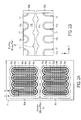
- FIG. 2A illustrates an example layout of the vertical HVFET structure shown in Figure 1 .
- the top view of Figure 2A shows a single, discrete HVFET comprising an upper transistor section 30a and a lower transistor section 30b on a semiconductor die 21. The two sections are separated by a dummy silicon pillar 32.
- Each section 30 comprises a plurality of "racetrack" shaped transistor structures or segments, each transistor segment comprises an elongated ring or oval that includes a silicon pillar 17 surrounded on opposite sides by dielectric regions 15a & 15b. Pillar 17, itself, extends laterally in the x and y directions to form a continuous, elongated, racetrack-shaped ring or oval.
- Field plate 19a comprises a single elongated member that terminates on either end in a rounded fingertip area.
- Field plate 19b comprises an enlarged ring or oval that encircles pillar 17.
- Field plates 19b of adjacent racetrack structures are shown merged such that they share a common member on a side.
- the cross-sectional view of Figure 1 may be taken through cut lines A-A' of the example layout of Figure 2A .
- each of the racetrack transistor segments has a width (i.e., pitch) in the y-direction of approximately 13 ⁇ m, a length in the x-direction in a range of about 400 ⁇ m to 1000 ⁇ m, with a pillar height of about 60 ⁇ m.
- the length to width ratio of the individual racetrack transistor segments comprising sections 30a & 30b is in a range of about 30 up to 80.
- the length of each racetrack shaped segment is at least 20 times greater than its pitch or width.
- patterned metal layers are used to interconnect each of the silicon pillars 17 of the individual transistor segments. That is, in a practical embodiment, all of the source regions, gate members, and field plates are respectively wired together to corresponding electrodes on the die.
- the transistor segments in each section 30 are arranged in a side-by-side relationship in the y-direction substantially across a width of die 21.
- the additive length of the transistor segments of sections 30a & 30b extend substantially over the length of die 21.
- the width of dielectric regions 15 separating the silicon pillars, as well as the width of the field plates is substantially uniform across semiconductor die 21. Laying out the transistor segments with uniform widths and separation distances prevents the formation of voids or holes following the processing steps used to conformably deposit the layers that comprise dielectric regions 15 and field plates 19.
- Figure 2B is an expanded view of one portion of the example layout shown in Figure 2A .
- Dummy silicon pillar 32 is shown separating the rounded end areas of dielectric regions 15b of respective transistor segment sections 30a & 30b.
- the deep vertical trenches that are etched in the semiconductor substrate to define pillars 17 also define dummy silicon pillar 32.
- dummy silicon pillar 32 is made to have a width in the x-direction (i.e., that separates the transistor segment sections) that is as small as can be reliably manufactured.
- segmenting the single die HVFET into sections separated by dummy silicon pillar 32 is to introduce lengthwise (x-direction) stress-relief in the elongated racetrack shaped transistor segments. Segmenting or breaking the transistor device structures into two or more sections relieves mechanical stress across the length of the die. This stress is induced by the oxide regions flanking the pillars and normally concentrates at the rounded ends of each racetrack segment. Relieving mechanical stress by segmenting the transistor device structures into two or more sections thus prevents undesirable warping of the silicon pillars and damage (e.g., dislocations) to the silicon caused by stress.
- damage e.g., dislocations
- a dummy pillar of silicon instead of a dummy pillar of silicon to separate pairs of racetrack transistor segments, each pair being located in a different section, a dummy pillar comprising a different material may be utilized.
- the material used for the dummy pillar should have a thermal coefficient of expansion close to that of silicon, or sufficiently different from that of the dielectric region so as to relieve the lengthwise stress induced by the dielectric regions flanking the silicon pillars.
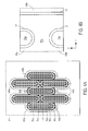
- Figure 3A illustrates another example layout of the vertical HVFET structure shown in Figure 1 .
- Figure 3B is an expanded view of one portion of the example layout shown in Figure 3A , just showing pillars 17, oxide region 15b, and an optional dummy silicon pillar 33.
- Figures 3A & 3B show a single, discrete HVFET comprising an upper transistor section 30a and a lower transistor section 30b on a semiconductor die 21.
- the deep vertical trenches filled with oxide regions 15b and field plates 19b of transistor sections 30a and 30b overlap, or are merged, leaving small, diamond-shaped dummy silicon pillars 33 between the segmented transistor sections.
- a single dummy pillar is centrally located between the four rounded ends of adjacent pairs of transistor segments over the two sections.
- N is an integer greater than 1
- racetrack segments or structures in a section 30 of the transistor comprising die 21 there are a total of N-1 dummy pillars 33.
- Figure 4A illustrates yet another example layout of the vertical HVFET structure shown in Figure 1 .
- Figure 4B is an expanded view of one portion of the example layout shown in Figure 4A . Pillars 17 and oxide region 15b are just shown for clarity reasons in the expanded view of Figure 4B .
- the transistor segments comprising the HVFET of semiconductor die 21 are alternately shifted by half of the length of each racetrack segment, resulting in racetrack transistor segments that are alternately associated with upper transistor section 40a and lower transistor section 40b.
- each of the transistor segments of a row of section 40a is separated by a pair of the transistor segments of section 40b, the pair being arranged in an end-to-end relationship in the x-direction.
- alternate shifting of the segments may be any fraction of the segment length. In other words, shifting of the segments is not limited to 50% or half the length. Various embodiments may comprise segments alternately shifted by any percentage or fraction ranging from greater than 0% to less than 100% of the length of the transistor segments.
- the dielectric regions 15b of alternating ones of the transistor segments in respective sections 40a & 40b are merged.
- the rounded ends of the transistor segments associated with different adjacent sections overlap or are merged such that field plates 19b of the adjacent sections are merged at the ends (in the x-direction).
- the extended straight side portions of field plates 19b of alternating transistor segments of different sections are merged along a substantial length of each segment. It is appreciated that regions 15b and 19b may be merged with or without a dummy pillar (or isolated dummy silicon pillars) between the respective sections.
- FIG 5 illustrates an example layout of a wafer 50 with die-to-die checkerboarding of HVFETs 10a-10d on semiconductor die 21a-21d, respectively.
- HVFETs 10 comprises a plurality of racetrack-shaped transistor segments such as that shown in Figure 1 , arranged side-by-side along their width into a substantially square block.
- HVFETs 10a-10d each comprises transistor segments having a length that extends substantially across the length of the respective die 21a-21d.
- the width of each segment is about 13 ⁇ m, with the length ranging from about 500 ⁇ m to 2000 ⁇ m. Other embodiments may have lengths greater than 2000 ⁇ m.
- the block or stacked arrangement of segments also extends substantially across the width of each die.
- each die 21 represents the edge of the scribe area between adjacent semiconductor die.
- Figure 5 shows two rows and two columns of HVFETs 10 it is appreciated that the die-to-die checkerboarding arrangement shown may be repeated across the entire wafer substrate.
- adjacent die in a row or a column are oriented such that the length of the transistor segments in one die extends in one direction, with the length of the transistor segments in an adjacent die extending in a second orthogonal direction.
- HVFET 10a is shown with the length of its transistor segments oriented in the x-direction, whereas adjacent HVFETs 10b & 10c
- By orthogonal alternating the orientation of the transistor segments in each individual die 21 across wafer 50 i.e., checkerboarding
- mechanical stress generated by the long dielectric regions is distributed in two orthogonal directions, thus reducing warping of wafer 50.
- Figure 6 illustrates another example layout of a wafer with die-to-die checkerboarding of segmented HVFETs.
- the example of Figure 6 utilizes the same approach as in Figure 5 of alternating the orientation of the transistor structures die-to-die; however, in the embodiment of Figure 6 , the HVFET structures are segmented into multiple (e.g., two) sections. For instance, each HVFET that extends substantially across the length and width of a semiconductor die 21 is segmented into two sections 30a & 30b separated by a dummy pillar 32.
- Each of the semiconductor die 21 shown in Figure 6 has a layout that is the same as that shown in Figure 2A for a substantially square die. Similar to the example shown in Figure 5 , adjacent die have transistor segments that are orthogonally alternating across wafer 50. That is, the transistor segments in sections 30a & 30b of die 21 a and 21 d have a length oriented in the x-direction, whereas the transistor segments in sections 30a & 30b of die 21 b and 21 c have a length oriented in the y-direction.
- the HVFET of each die 21 may be formed with multiple transistor sections, e.g., greater than 2, each separated by one or more dummy pillars.
- any of the single die layouts with multiple transistor sections shown in the examples of Figures 2A-4B may be utilized in each of the die 21 shown in Figure 6 , with the orientation of the segments alternating die-to-die across wafer 50.
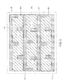
- Figure 7 illustrates an example rectangular layout of a die 25 with checkerboarded blocks of racetrack-shaped HVFET segments stacked in a side-by-side arrangement of substantially square blocks or sections 36.
- Adjacent sections in a row or a column are oriented such that the length of the transistor segments in one section extends in one direction, with the length of the transistor segments in the other adjacent section extending in a second orthogonal direction.
- each of the rows and columns of die 25 include transistor sections 36a oriented with the elongated transistor segments aligned in the x-direction and alternate transistor sections 36b oriented with the elongated transistor segments aligned in the y-direction.
- the spaces between sections 36a and 36b comprise dummy silicon pillars; that is, the silicon that forms the dummy pillars is not an active transistor region.
- die 25 comprises three rows and four columns of transistor sections 36.
- the checkerboarded layout approach shown in the example of Figure 7 may be used to produce a single, discrete HVFET on a die of virtually any (within practical limits) rectilinear-shape.
- Figure 8 illustrates an example gate metal routing layout for the die shown in Figure 7 .
- the gate metal routing scheme of Figure 8 is fabricated using a single metal layer process with both source and gate metal disposed on the same planar level.
- the example shown includes horizontal gate metal bus lines 41a-41d that run between each row of the checkerboarded blocks of racetrack-shaped HVFET segments.
- gate metal bus lines 41 a & 41 b are shown extending horizontally along the top and bottom of the first (upper) row of checkerboarded sections 36 of Figure 7 . (It is appreciated that gate metal bus line 41 b may be twice as wide as bus line 41a due to the face that bus line 41 b provides a shared conduction path to the polysilicon gate members of both the first and second rows of checkerboarded sections.)
- each row the sections 36 that have the length of their transistor segments aligned in the x-direction have half of the polysilicon gate members coupled to the top bus line, and a second half of the polysilicon gate members coupled to the bottom bus line,
- the upper left-hand block or section 36 in Figure 8 is shown having the polysilicon gate members represented by lines 44a connected to gate metal bus line 41 b via contacts 45a, whereas the polysilicon gate members represented by lines 44b in the same section are connected to gate metal bus line 41a via contacts 45b.
- each line 44a or 44b actually represents the two gate members 18a & 18b (see Figure 1 ) of a single racetrack-shaped HVFET segment.
- lines 44a represent the gate members of the two left-most HVFET segments
- lines 44b represent the gate members of the two right-most HVFET segments, in the same section. Note further that each gate member is connected to a bus line (top or bottom) at one end only.
- the gate metal routing pattern shown in Figure 8 also includes vertical gate metal stub lines 42 that extend approximately half-way across each row of checkerboarded blocks. Within each section in which the length of the HVFET segments is aligned in the y-direction, half of the polysilicon gate members are coupled to one stub line, and the other half of the polysilicon gate members are coupled to another stub line.
- the second section (from the left) in the upper row of Figure 8 shows a bottom half of the gate members (represented by lines 44c) connected to left-sided gate metal stub line 42a via contacts 45c, with a top half of the gate members (represented by lines 44d) connected to right-sided gate metal stub line 42b via contacts 45d.
- the fourth section (right-hand most) in the upper row of Figure 8 shows a bottom half of the gate members connected to gate metal stub line 42c and a top half of the gate members connected to gate metal stub line 42d. Note that each gate member of the horizontally-aligned segments is connected to a stub line (left or right side) at one end only.
- gate metal stub lines 42 extend only half-way across those sections having their segments aligned in the y-direction (i.e., horizontally) is to allow the source metal bus lines to extend across each row and contact the source regions of each transistor segment.
- Figure 9 shows a die 25 having individual source bus lines 61 that extend continuously across each row of transistor sections 36 between top and bottom gate metal traces 51.
- Metal traces 51 represent the merged metal bus lines 41 and stub lines 42 associated with each row.
- source bus lines 61 a runs continuously across the upper row of sections on die 25 to contact each of the source regions 14 at the top of silicon pillars 17 for each HVFET segment in the row. In so doing, source bus lines 61a "snakes" between and around stub lines 42, as well as between bus lines 41, all of which are patterned on the same single layer of metal.
- Figure 10 illustrates an expanded portion of the example layout shown in Figure 9 that shows one possible scheme for connecting gate metal trace 51 with gate members 18a & 18b.
- via contacts 55a & 55b are shown connecting trace 51 with the rounded fingertip portion of gate members 18a & 18b, respectively.
- the source region at the top of pillar 17 located between gate members 18a & 18b is shown connected to source metal bus 61 via contacts 75.
- gate metal trace 51 may connect along the straight, linear portion of gate members 18a & 18b near the rounded fingertip portion. (Note that the field plates are not shown in the example of Figure 10 for clarity reasons.)
Landscapes
- Semiconductor Integrated Circuits (AREA)
- Junction Field-Effect Transistors (AREA)
- Metal-Oxide And Bipolar Metal-Oxide Semiconductor Integrated Circuits (AREA)
- Thin Film Transistor (AREA)
- Electrodes Of Semiconductors (AREA)
- Insulated Gate Type Field-Effect Transistor (AREA)
Priority Applications (1)
| Application Number | Priority Date | Filing Date | Title |
|---|---|---|---|
| EP20130152055 EP2587545A1 (de) | 2007-02-16 | 2007-11-28 | Vertikaler Hochspannung-FET und Verfahren zu dessen Herstellung |
Applications Claiming Priority (2)
| Application Number | Priority Date | Filing Date | Title |
|---|---|---|---|
| US11/707,403 US7468536B2 (en) | 2007-02-16 | 2007-02-16 | Gate metal routing for transistor with checkerboarded layout |
| EP07254619A EP1959500B1 (de) | 2007-02-16 | 2007-11-28 | Vertikaler Hochspannung-FET und Verfahren zu dessen Herstellung |
Related Parent Applications (1)
| Application Number | Title | Priority Date | Filing Date |
|---|---|---|---|
| EP07254619.5 Division | 2007-11-28 |
Publications (2)
| Publication Number | Publication Date |
|---|---|
| EP2365533A2 true EP2365533A2 (de) | 2011-09-14 |
| EP2365533A3 EP2365533A3 (de) | 2011-09-28 |
Family
ID=39322666
Family Applications (3)
| Application Number | Title | Priority Date | Filing Date |
|---|---|---|---|
| EP11168216A Withdrawn EP2365533A3 (de) | 2007-02-16 | 2007-11-28 | Vertikaler Hochspannung-FET und Verfahren zu dessen Herstellung |
| EP07254619A Not-in-force EP1959500B1 (de) | 2007-02-16 | 2007-11-28 | Vertikaler Hochspannung-FET und Verfahren zu dessen Herstellung |
| EP20130152055 Withdrawn EP2587545A1 (de) | 2007-02-16 | 2007-11-28 | Vertikaler Hochspannung-FET und Verfahren zu dessen Herstellung |
Family Applications After (2)
| Application Number | Title | Priority Date | Filing Date |
|---|---|---|---|
| EP07254619A Not-in-force EP1959500B1 (de) | 2007-02-16 | 2007-11-28 | Vertikaler Hochspannung-FET und Verfahren zu dessen Herstellung |
| EP20130152055 Withdrawn EP2587545A1 (de) | 2007-02-16 | 2007-11-28 | Vertikaler Hochspannung-FET und Verfahren zu dessen Herstellung |
Country Status (5)
| Country | Link |
|---|---|
| US (2) | US7468536B2 (de) |
| EP (3) | EP2365533A3 (de) |
| JP (2) | JP2008205484A (de) |
| CN (2) | CN101246907B (de) |
| AT (1) | ATE513315T1 (de) |
Cited By (1)
| Publication number | Priority date | Publication date | Assignee | Title |
|---|---|---|---|---|
| US10957599B2 (en) | 2018-11-07 | 2021-03-23 | International Business Machines Corporation | Integrating extra gate VFET with single gate VFET |
Families Citing this family (38)
| Publication number | Priority date | Publication date | Assignee | Title |
|---|---|---|---|---|
| US6573558B2 (en) * | 2001-09-07 | 2003-06-03 | Power Integrations, Inc. | High-voltage vertical transistor with a multi-layered extended drain structure |
| US7786533B2 (en) | 2001-09-07 | 2010-08-31 | Power Integrations, Inc. | High-voltage vertical transistor with edge termination structure |
| US6635544B2 (en) | 2001-09-07 | 2003-10-21 | Power Intergrations, Inc. | Method of fabricating a high-voltage transistor with a multi-layered extended drain structure |
| US7135748B2 (en) * | 2004-10-26 | 2006-11-14 | Power Integrations, Inc. | Integrated circuit with multi-length output transistor segment |
| US8093621B2 (en) | 2008-12-23 | 2012-01-10 | Power Integrations, Inc. | VTS insulated gate bipolar transistor |
| US7595523B2 (en) | 2007-02-16 | 2009-09-29 | Power Integrations, Inc. | Gate pullback at ends of high-voltage vertical transistor structure |
| US7859037B2 (en) * | 2007-02-16 | 2010-12-28 | Power Integrations, Inc. | Checkerboarded high-voltage vertical transistor layout |
| US7557406B2 (en) | 2007-02-16 | 2009-07-07 | Power Integrations, Inc. | Segmented pillar layout for a high-voltage vertical transistor |
| US7468536B2 (en) * | 2007-02-16 | 2008-12-23 | Power Integrations, Inc. | Gate metal routing for transistor with checkerboarded layout |
| US8653583B2 (en) | 2007-02-16 | 2014-02-18 | Power Integrations, Inc. | Sensing FET integrated with a high-voltage transistor |
| US7875962B2 (en) * | 2007-10-15 | 2011-01-25 | Power Integrations, Inc. | Package for a power semiconductor device |
| US7964912B2 (en) | 2008-09-18 | 2011-06-21 | Power Integrations, Inc. | High-voltage vertical transistor with a varied width silicon pillar |
| US7871882B2 (en) | 2008-12-20 | 2011-01-18 | Power Integrations, Inc. | Method of fabricating a deep trench insulated gate bipolar transistor |
| US20100155831A1 (en) * | 2008-12-20 | 2010-06-24 | Power Integrations, Inc. | Deep trench insulated gate bipolar transistor |
| US8207455B2 (en) * | 2009-07-31 | 2012-06-26 | Power Integrations, Inc. | Power semiconductor package with bottom surface protrusions |
| US8115457B2 (en) | 2009-07-31 | 2012-02-14 | Power Integrations, Inc. | Method and apparatus for implementing a power converter input terminal voltage discharge circuit |
| US8207577B2 (en) * | 2009-09-29 | 2012-06-26 | Power Integrations, Inc. | High-voltage transistor structure with reduced gate capacitance |
| US7893754B1 (en) | 2009-10-02 | 2011-02-22 | Power Integrations, Inc. | Temperature independent reference circuit |
| US8634218B2 (en) * | 2009-10-06 | 2014-01-21 | Power Integrations, Inc. | Monolithic AC/DC converter for generating DC supply voltage |
| US9306056B2 (en) | 2009-10-30 | 2016-04-05 | Vishay-Siliconix | Semiconductor device with trench-like feed-throughs |
| US8310845B2 (en) | 2010-02-10 | 2012-11-13 | Power Integrations, Inc. | Power supply circuit with a control terminal for different functional modes of operation |
| JP2012204529A (ja) * | 2011-03-24 | 2012-10-22 | Toshiba Corp | 半導体装置及びその製造方法 |
| US8653600B2 (en) | 2012-06-01 | 2014-02-18 | Power Integrations, Inc. | High-voltage monolithic schottky device structure |
| US9455621B2 (en) | 2013-08-28 | 2016-09-27 | Power Integrations, Inc. | Controller IC with zero-crossing detector and capacitor discharge switching element |
| US10325988B2 (en) | 2013-12-13 | 2019-06-18 | Power Integrations, Inc. | Vertical transistor device structure with cylindrically-shaped field plates |
| US9543396B2 (en) | 2013-12-13 | 2017-01-10 | Power Integrations, Inc. | Vertical transistor device structure with cylindrically-shaped regions |
| US9667154B2 (en) | 2015-09-18 | 2017-05-30 | Power Integrations, Inc. | Demand-controlled, low standby power linear shunt regulator |
| US9973183B2 (en) | 2015-09-28 | 2018-05-15 | Power Integrations, Inc. | Field-effect transistor device with partial finger current sensing FETs |
| US9602009B1 (en) | 2015-12-08 | 2017-03-21 | Power Integrations, Inc. | Low voltage, closed loop controlled energy storage circuit |
| US9629218B1 (en) | 2015-12-28 | 2017-04-18 | Power Integrations, Inc. | Thermal protection for LED bleeder in fault condition |
| US9983239B2 (en) | 2016-05-13 | 2018-05-29 | Power Integrations, Inc. | Integrated linear current sense circuitry for semiconductor transistor devices |
| WO2018030990A1 (en) | 2016-08-08 | 2018-02-15 | Power Integrations, Inc. | Integrated circuit fast temperature sensing of a semiconductor switching device |
| US10622476B2 (en) | 2017-12-27 | 2020-04-14 | Samsung Electronics Co., Ltd. | Vertical field effect transistor having two-dimensional channel structure |
| US11018250B2 (en) | 2019-05-06 | 2021-05-25 | Infineon Technologies Ag | Semiconductor device with multi-branch gate contact structure |
| CN114503279A (zh) * | 2019-08-12 | 2022-05-13 | 麦斯功率半导体股份有限公司 | 具选择性屏蔽式凹陷场效电板的高密度功率元件 |
| GB2587646B (en) * | 2019-10-03 | 2022-08-03 | Mqsemi Ag | Semiconductor device with dual trench structure |
| WO2022201903A1 (ja) * | 2021-03-22 | 2022-09-29 | ローム株式会社 | 半導体装置 |
| TWI825508B (zh) * | 2021-11-11 | 2023-12-11 | 力晶積成電子製造股份有限公司 | 半導體結構 |
Citations (1)
| Publication number | Priority date | Publication date | Assignee | Title |
|---|---|---|---|---|
| US6337498B1 (en) * | 1998-02-12 | 2002-01-08 | Kabushiki Kaisha Toshiba | Semiconductor device having directionally balanced gates and manufacturing method |
Family Cites Families (133)
| Publication number | Priority date | Publication date | Assignee | Title |
|---|---|---|---|---|
| JPS5712557Y2 (de) | 1974-12-20 | 1982-03-12 | ||
| JPS53125657A (en) | 1977-04-09 | 1978-11-02 | Hoshizaki Electric Co Ltd | Detecting system for completion of deicing in automatic ice machine |
| JPS5710975Y2 (de) | 1977-05-31 | 1982-03-03 | ||
| JPS5712558Y2 (de) | 1977-06-15 | 1982-03-12 | ||
| US4343015A (en) | 1980-05-14 | 1982-08-03 | General Electric Company | Vertical channel field effect transistor |
| GB2089119A (en) | 1980-12-10 | 1982-06-16 | Philips Electronic Associated | High voltage semiconductor devices |
| US4626879A (en) | 1982-12-21 | 1986-12-02 | North American Philips Corporation | Lateral double-diffused MOS transistor devices suitable for source-follower applications |
| JPS59155144A (ja) * | 1983-02-24 | 1984-09-04 | Toshiba Corp | 半導体集積回路装置 |
| US4738936A (en) | 1983-07-01 | 1988-04-19 | Acrian, Inc. | Method of fabrication lateral FET structure having a substrate to source contact |
| US4626789A (en) | 1983-08-19 | 1986-12-02 | Hitachi, Ltd. | Demodulating circuit for data signal |
| JPS6064471A (ja) | 1983-09-19 | 1985-04-13 | Nec Corp | 高電圧絶縁ゲ−ト型電界効果トランジスタ |
| US4531173A (en) | 1983-11-02 | 1985-07-23 | Motorola, Inc. | Protective power foldback circuit for a power semiconductor |
| US4618541A (en) | 1984-12-21 | 1986-10-21 | Advanced Micro Devices, Inc. | Method of forming a silicon nitride film transparent to ultraviolet radiation and resulting article |
| JPS61168253A (ja) | 1985-01-19 | 1986-07-29 | Sharp Corp | 高耐圧mos電界効果半導体装置 |
| US4665426A (en) | 1985-02-01 | 1987-05-12 | Advanced Micro Devices, Inc. | EPROM with ultraviolet radiation transparent silicon nitride passivation layer |
| US4963951A (en) | 1985-11-29 | 1990-10-16 | General Electric Company | Lateral insulated gate bipolar transistors with improved latch-up immunity |
| US4764800A (en) | 1986-05-07 | 1988-08-16 | Advanced Micro Devices, Inc. | Seal structure for an integrated circuit |
| US4796070A (en) | 1987-01-15 | 1989-01-03 | General Electric Company | Lateral charge control semiconductor device and method of fabrication |
| US5010024A (en) | 1987-03-04 | 1991-04-23 | Advanced Micro Devices, Inc. | Passivation for integrated circuit structures |
| US4811075A (en) | 1987-04-24 | 1989-03-07 | Power Integrations, Inc. | High voltage MOS transistors |
| US4890144A (en) | 1987-09-14 | 1989-12-26 | Motorola, Inc. | Integrated circuit trench cell |
| JPS63314847A (ja) * | 1987-06-17 | 1988-12-22 | Nec Corp | マスタ−スライス型半導体装置 |
| JPH01112764A (ja) | 1987-10-27 | 1989-05-01 | Nec Corp | 半導体装置 |
| US4939566A (en) | 1987-10-30 | 1990-07-03 | North American Philips Corporation | Semiconductor switch with parallel DMOS and IGT |
| US4926074A (en) | 1987-10-30 | 1990-05-15 | North American Philips Corporation | Semiconductor switch with parallel lateral double diffused MOS transistor and lateral insulated gate transistor |
| US4890146A (en) | 1987-12-16 | 1989-12-26 | Siliconix Incorporated | High voltage level shift semiconductor device |
| US4922327A (en) | 1987-12-24 | 1990-05-01 | University Of Toronto Innovations Foundation | Semiconductor LDMOS device with upper and lower passages |
| US4929987A (en) | 1988-02-01 | 1990-05-29 | General Instrument Corporation | Method for setting the threshold voltage of a power mosfet |
| US5025296A (en) | 1988-02-29 | 1991-06-18 | Motorola, Inc. | Center tapped FET |
| JP2619466B2 (ja) | 1988-03-18 | 1997-06-11 | 株式会社日立製作所 | 半導体装置、半導体装置の設計支援システム及び半導体装置を用いた電源システム |
| US5283201A (en) | 1988-05-17 | 1994-02-01 | Advanced Power Technology, Inc. | High density power device fabrication process |
| US5237193A (en) | 1988-06-24 | 1993-08-17 | Siliconix Incorporated | Lightly doped drain MOSFET with reduced on-resistance |
| EP0371785B1 (de) | 1988-11-29 | 1996-05-01 | Kabushiki Kaisha Toshiba | Lateraler Leitfähigkeitsmodulations-MOSFET |
| US5072266A (en) | 1988-12-27 | 1991-12-10 | Siliconix Incorporated | Trench DMOS power transistor with field-shaping body profile and three-dimensional geometry |
| JP2877408B2 (ja) | 1990-01-12 | 1999-03-31 | 株式会社東芝 | 導電変調型mosfet |
| JP2597412B2 (ja) | 1990-03-20 | 1997-04-09 | 三菱電機株式会社 | 半導体装置およびその製造方法 |
| US5040045A (en) | 1990-05-17 | 1991-08-13 | U.S. Philips Corporation | High voltage MOS transistor having shielded crossover path for a high voltage connection bus |
| JP2599493B2 (ja) | 1990-08-27 | 1997-04-09 | 松下電子工業株式会社 | 半導体装置 |
| US5122848A (en) | 1991-04-08 | 1992-06-16 | Micron Technology, Inc. | Insulated-gate vertical field-effect transistor with high current drive and minimum overlap capacitance |
| US5386136A (en) | 1991-05-06 | 1995-01-31 | Siliconix Incorporated | Lightly-doped drain MOSFET with improved breakdown characteristics |
| US5146298A (en) | 1991-08-16 | 1992-09-08 | Eklund Klas H | Device which functions as a lateral double-diffused insulated gate field effect transistor or as a bipolar transistor |
| US5258636A (en) | 1991-12-12 | 1993-11-02 | Power Integrations, Inc. | Narrow radius tips for high voltage semiconductor devices with interdigitated source and drain electrodes |
| US5270264A (en) | 1991-12-20 | 1993-12-14 | Intel Corporation | Process for filling submicron spaces with dielectric |
| JP2748072B2 (ja) * | 1992-07-03 | 1998-05-06 | 三菱電機株式会社 | 半導体装置およびその製造方法 |
| JP3435173B2 (ja) | 1992-07-10 | 2003-08-11 | 株式会社日立製作所 | 半導体装置 |
| US5294824A (en) | 1992-07-31 | 1994-03-15 | Motorola, Inc. | High voltage transistor having reduced on-resistance |
| JP3158738B2 (ja) | 1992-08-17 | 2001-04-23 | 富士電機株式会社 | 高耐圧mis電界効果トランジスタおよび半導体集積回路 |
| JP3205099B2 (ja) | 1992-12-25 | 2001-09-04 | 株式会社日立製作所 | 半導体集積回路装置 |
| US5326711A (en) | 1993-01-04 | 1994-07-05 | Texas Instruments Incorporated | High performance high voltage vertical transistor and method of fabrication |
| JP3076468B2 (ja) | 1993-01-26 | 2000-08-14 | 松下電子工業株式会社 | 半導体装置 |
| US5313082A (en) | 1993-02-16 | 1994-05-17 | Power Integrations, Inc. | High voltage MOS transistor with a low on-resistance |
| DE4309764C2 (de) | 1993-03-25 | 1997-01-30 | Siemens Ag | Leistungs-MOSFET |
| US5349225A (en) | 1993-04-12 | 1994-09-20 | Texas Instruments Incorporated | Field effect transistor with a lightly doped drain |
| US5324683A (en) | 1993-06-02 | 1994-06-28 | Motorola, Inc. | Method of forming a semiconductor structure having an air region |
| BE1007283A3 (nl) | 1993-07-12 | 1995-05-09 | Philips Electronics Nv | Halfgeleiderinrichting met een most voorzien van een extended draingebied voor hoge spanningen. |
| ATE175523T1 (de) | 1993-09-17 | 1999-01-15 | Cons Ric Microelettronica | Eine integrierte vorrichtung mit einem bipolaren transistor und einem mosfet transistor in emittorschaltungsanordnung |
| US5523604A (en) | 1994-05-13 | 1996-06-04 | International Rectifier Corporation | Amorphous silicon layer for top surface of semiconductor device |
| US5494853A (en) | 1994-07-25 | 1996-02-27 | United Microelectronics Corporation | Method to solve holes in passivation by metal layout |
| US5521105A (en) | 1994-08-12 | 1996-05-28 | United Microelectronics Corporation | Method of forming counter-doped island in power MOSFET |
| US5550405A (en) | 1994-12-21 | 1996-08-27 | Advanced Micro Devices, Incorporated | Processing techniques for achieving production-worthy, low dielectric, low interconnect resistance and high performance ICS |
| US5656543A (en) | 1995-02-03 | 1997-08-12 | National Semiconductor Corporation | Fabrication of integrated circuits with borderless vias |
| DE69602114T2 (de) | 1995-02-10 | 1999-08-19 | Siliconix Inc. | Graben-Feldeffekttransistor mit PN-Verarmungsschicht-Barriere |
| JP3291958B2 (ja) | 1995-02-21 | 2002-06-17 | 富士電機株式会社 | バックソースmosfet |
| US5670828A (en) | 1995-02-21 | 1997-09-23 | Advanced Micro Devices, Inc. | Tunneling technology for reducing intra-conductive layer capacitance |
| US5798554A (en) * | 1995-02-24 | 1998-08-25 | Consorzio Per La Ricerca Sulla Microelettronica Nel Mezzogiorno | MOS-technology power device integrated structure and manufacturing process thereof |
| US6049108A (en) | 1995-06-02 | 2000-04-11 | Siliconix Incorporated | Trench-gated MOSFET with bidirectional voltage clamping |
| US6204533B1 (en) * | 1995-06-02 | 2001-03-20 | Siliconix Incorporated | Vertical trench-gated power MOSFET having stripe geometry and high cell density |
| US5659201A (en) | 1995-06-05 | 1997-08-19 | Advanced Micro Devices, Inc. | High conductivity interconnection line |
| KR100188096B1 (ko) | 1995-09-14 | 1999-06-01 | 김광호 | 반도체 장치 및 그 제조 방법 |
| US5637898A (en) | 1995-12-22 | 1997-06-10 | North Carolina State University | Vertical field effect transistors having improved breakdown voltage capability and low on-state resistance |
| JPH09266311A (ja) | 1996-01-22 | 1997-10-07 | Fuji Electric Co Ltd | 半導体装置及びその製造方法 |
| US6097063A (en) | 1996-01-22 | 2000-08-01 | Fuji Electric Co., Ltd. | Semiconductor device having a plurality of parallel drift regions |
| EP1039548B1 (de) | 1996-02-05 | 2004-03-31 | Infineon Technologies AG | Durch Feldeffekt steuerbares Halbleiterbauelement |
| DE19611045C1 (de) | 1996-03-20 | 1997-05-22 | Siemens Ag | Durch Feldeffekt steuerbares Halbleiterbauelement |
| AU3724197A (en) | 1996-07-19 | 1998-02-10 | Siliconix Incorporated | High density trench dmos transistor with trench bottom implant |
| US5841166A (en) | 1996-09-10 | 1998-11-24 | Spectrian, Inc. | Lateral DMOS transistor for RF/microwave applications |
| US6207994B1 (en) | 1996-11-05 | 2001-03-27 | Power Integrations, Inc. | High-voltage transistor with multi-layer conduction region |
| KR100228331B1 (ko) | 1996-12-30 | 1999-11-01 | 김영환 | 반도체 소자의 삼중웰 제조 방법 |
| DE69728852D1 (de) | 1997-01-31 | 2004-06-03 | St Microelectronics Srl | Verfahren zur Herstellung von einer morphologischen Randstruktur um ein integriertes elektronisches Bauelement zu versiegeln, sowie ein entsprechendes Bauelement |
| JP3393544B2 (ja) | 1997-02-26 | 2003-04-07 | シャープ株式会社 | 半導体装置の製造方法 |
| US6133607A (en) | 1997-05-22 | 2000-10-17 | Kabushiki Kaisha Toshiba | Semiconductor device |
| US5869875A (en) | 1997-06-10 | 1999-02-09 | Spectrian | Lateral diffused MOS transistor with trench source contact |
| US6054752A (en) | 1997-06-30 | 2000-04-25 | Denso Corporation | Semiconductor device |
| US6194283B1 (en) | 1997-10-29 | 2001-02-27 | Advanced Micro Devices, Inc. | High density trench fill due to new spacer fill method including isotropically etching silicon nitride spacers |
| US6316807B1 (en) | 1997-12-05 | 2001-11-13 | Naoto Fujishima | Low on-resistance trench lateral MISFET with better switching characteristics and method for manufacturing same |
| JP2001513270A (ja) | 1997-12-24 | 2001-08-28 | コーニンクレッカ フィリップス エレクトロニクス エヌ ヴィ | 改良されたオン状態特性を有する高電圧薄膜トランジスタ及びその製造方法 |
| US6362064B2 (en) | 1998-04-21 | 2002-03-26 | National Semiconductor Corporation | Elimination of walkout in high voltage trench isolated devices |
| EP0961325B1 (de) * | 1998-05-26 | 2008-05-07 | STMicroelectronics S.r.l. | MOS-Technologie-Leistungsanordnung mit hoher Integrationsdichte |
| JP3016762B2 (ja) | 1998-06-25 | 2000-03-06 | 松下電子工業株式会社 | 半導体装置およびその製造方法 |
| US6037631A (en) * | 1998-09-18 | 2000-03-14 | Siemens Aktiengesellschaft | Semiconductor component with a high-voltage endurance edge structure |
| US5998833A (en) | 1998-10-26 | 1999-12-07 | North Carolina State University | Power semiconductor devices having improved high frequency switching and breakdown characteristics |
| US6621121B2 (en) | 1998-10-26 | 2003-09-16 | Silicon Semiconductor Corporation | Vertical MOSFETs having trench-based gate electrodes within deeper trench-based source electrodes |
| DE19854915C2 (de) | 1998-11-27 | 2002-09-05 | Infineon Technologies Ag | MOS-Feldeffekttransistor mit Hilfselektrode |
| US6084277A (en) | 1999-02-18 | 2000-07-04 | Power Integrations, Inc. | Lateral power MOSFET with improved gate design |
| JP2000252465A (ja) | 1999-03-03 | 2000-09-14 | Sony Corp | 半導体装置およびその製造方法 |
| US6331455B1 (en) * | 1999-04-01 | 2001-12-18 | Advanced Power Devices, Inc. | Power rectifier device and method of fabricating power rectifier devices |
| US6191447B1 (en) | 1999-05-28 | 2001-02-20 | Micro-Ohm Corporation | Power semiconductor devices that utilize tapered trench-based insulating regions to improve electric field profiles in highly doped drift region mesas and methods of forming same |
| GB9917099D0 (en) | 1999-07-22 | 1999-09-22 | Koninkl Philips Electronics Nv | Cellular trench-gate field-effect transistors |
| JP3971062B2 (ja) | 1999-07-29 | 2007-09-05 | 株式会社東芝 | 高耐圧半導体装置 |
| US6365932B1 (en) | 1999-08-20 | 2002-04-02 | Denso Corporation | Power MOS transistor |
| US6127703A (en) | 1999-08-31 | 2000-10-03 | Philips Electronics North America Corporation | Lateral thin-film silicon-on-insulator (SOI) PMOS device having a drain extension region |
| JP4491875B2 (ja) * | 1999-12-13 | 2010-06-30 | 富士電機システムズ株式会社 | トレンチ型mos半導体装置 |
| US6489653B2 (en) | 1999-12-27 | 2002-12-03 | Kabushiki Kaisha Toshiba | Lateral high-breakdown-voltage transistor |
| GB0003185D0 (en) | 2000-02-12 | 2000-04-05 | Koninkl Philips Electronics Nv | An insulated gate field effect device |
| US6781194B2 (en) | 2001-04-11 | 2004-08-24 | Silicon Semiconductor Corporation | Vertical power devices having retrograded-doped transition regions and insulated trench-based electrodes therein |
| JP3448015B2 (ja) | 2000-07-26 | 2003-09-16 | 松下電器産業株式会社 | 半導体装置及びその製造方法 |
| CA2360031C (en) | 2000-10-30 | 2006-06-20 | Thomas & Betts International, Inc. | Capacitive test point voltage and phasing detector |
| US6649975B2 (en) | 2000-11-16 | 2003-11-18 | Silicon Semiconductor Corporation | Vertical power devices having trench-based electrodes therein |
| US6468847B1 (en) | 2000-11-27 | 2002-10-22 | Power Integrations, Inc. | Method of fabricating a high-voltage transistor |
| US6509220B2 (en) | 2000-11-27 | 2003-01-21 | Power Integrations, Inc. | Method of fabricating a high-voltage transistor |
| TW543146B (en) | 2001-03-09 | 2003-07-21 | Fairchild Semiconductor | Ultra dense trench-gated power device with the reduced drain-source feedback capacitance and miller charge |
| US6853033B2 (en) | 2001-06-05 | 2005-02-08 | National University Of Singapore | Power MOSFET having enhanced breakdown voltage |
| JP4421144B2 (ja) | 2001-06-29 | 2010-02-24 | 株式会社東芝 | 半導体装置 |
| JP4993824B2 (ja) * | 2001-07-03 | 2012-08-08 | ルネサスエレクトロニクス株式会社 | 半導体装置 |
| US7221011B2 (en) | 2001-09-07 | 2007-05-22 | Power Integrations, Inc. | High-voltage vertical transistor with a multi-gradient drain doping profile |
| US6635544B2 (en) | 2001-09-07 | 2003-10-21 | Power Intergrations, Inc. | Method of fabricating a high-voltage transistor with a multi-layered extended drain structure |
| US7786533B2 (en) * | 2001-09-07 | 2010-08-31 | Power Integrations, Inc. | High-voltage vertical transistor with edge termination structure |
| US6573558B2 (en) | 2001-09-07 | 2003-06-03 | Power Integrations, Inc. | High-voltage vertical transistor with a multi-layered extended drain structure |
| US6683344B2 (en) * | 2001-09-07 | 2004-01-27 | Ixys Corporation | Rugged and fast power MOSFET and IGBT |
| US6555873B2 (en) | 2001-09-07 | 2003-04-29 | Power Integrations, Inc. | High-voltage lateral transistor with a multi-layered extended drain structure |
| US6555883B1 (en) | 2001-10-29 | 2003-04-29 | Power Integrations, Inc. | Lateral power MOSFET for high switching speeds |
| US6552597B1 (en) | 2001-11-02 | 2003-04-22 | Power Integrations, Inc. | Integrated circuit with closely coupled high voltage output and offline transistor pair |
| DE10214151B4 (de) | 2002-03-28 | 2007-04-05 | Infineon Technologies Ag | Halbleiterbauelement mit erhöhter Durchbruchspannung im Randbereich |
| JP2004022700A (ja) | 2002-06-14 | 2004-01-22 | Sanyo Electric Co Ltd | 半導体装置 |
| US6865093B2 (en) | 2003-05-27 | 2005-03-08 | Power Integrations, Inc. | Electronic circuit control element with tap element |
| US7352036B2 (en) * | 2004-08-03 | 2008-04-01 | Fairchild Semiconductor Corporation | Semiconductor power device having a top-side drain using a sinker trench |
| US7135748B2 (en) | 2004-10-26 | 2006-11-14 | Power Integrations, Inc. | Integrated circuit with multi-length output transistor segment |
| JP5011843B2 (ja) * | 2006-06-22 | 2012-08-29 | 株式会社デンソー | 半導体装置 |
| US7859037B2 (en) * | 2007-02-16 | 2010-12-28 | Power Integrations, Inc. | Checkerboarded high-voltage vertical transistor layout |
| US7468536B2 (en) * | 2007-02-16 | 2008-12-23 | Power Integrations, Inc. | Gate metal routing for transistor with checkerboarded layout |
| US7595523B2 (en) * | 2007-02-16 | 2009-09-29 | Power Integrations, Inc. | Gate pullback at ends of high-voltage vertical transistor structure |
| US7557406B2 (en) * | 2007-02-16 | 2009-07-07 | Power Integrations, Inc. | Segmented pillar layout for a high-voltage vertical transistor |
| US8653583B2 (en) * | 2007-02-16 | 2014-02-18 | Power Integrations, Inc. | Sensing FET integrated with a high-voltage transistor |
-
2007
- 2007-02-16 US US11/707,403 patent/US7468536B2/en active Active
- 2007-11-28 EP EP11168216A patent/EP2365533A3/de not_active Withdrawn
- 2007-11-28 EP EP07254619A patent/EP1959500B1/de not_active Not-in-force
- 2007-11-28 EP EP20130152055 patent/EP2587545A1/de not_active Withdrawn
- 2007-11-28 AT AT07254619T patent/ATE513315T1/de not_active IP Right Cessation
-
2008
- 2008-02-15 JP JP2008064895A patent/JP2008205484A/ja active Pending
- 2008-02-18 CN CN2008100807532A patent/CN101246907B/zh active Active
- 2008-02-18 CN CN201110119758.3A patent/CN102201344B/zh not_active Expired - Fee Related
- 2008-11-12 US US12/291,569 patent/US7732860B2/en active Active
-
2013
- 2013-02-04 JP JP2013019567A patent/JP5637571B2/ja not_active Expired - Fee Related
Patent Citations (1)
| Publication number | Priority date | Publication date | Assignee | Title |
|---|---|---|---|---|
| US6337498B1 (en) * | 1998-02-12 | 2002-01-08 | Kabushiki Kaisha Toshiba | Semiconductor device having directionally balanced gates and manufacturing method |
Cited By (1)
| Publication number | Priority date | Publication date | Assignee | Title |
|---|---|---|---|---|
| US10957599B2 (en) | 2018-11-07 | 2021-03-23 | International Business Machines Corporation | Integrating extra gate VFET with single gate VFET |
Also Published As
| Publication number | Publication date |
|---|---|
| JP2008205484A (ja) | 2008-09-04 |
| EP1959500A3 (de) | 2009-06-03 |
| CN101246907A (zh) | 2008-08-20 |
| CN101246907B (zh) | 2011-06-22 |
| US20090072302A1 (en) | 2009-03-19 |
| EP1959500A2 (de) | 2008-08-20 |
| EP1959500B1 (de) | 2011-06-15 |
| JP2013080976A (ja) | 2013-05-02 |
| CN102201344B (zh) | 2014-01-15 |
| ATE513315T1 (de) | 2011-07-15 |
| CN102201344A (zh) | 2011-09-28 |
| US7468536B2 (en) | 2008-12-23 |
| US7732860B2 (en) | 2010-06-08 |
| EP2587545A1 (de) | 2013-05-01 |
| EP2365533A3 (de) | 2011-09-28 |
| US20080197396A1 (en) | 2008-08-21 |
| JP5637571B2 (ja) | 2014-12-10 |
Similar Documents
| Publication | Publication Date | Title |
|---|---|---|
| EP1959500B1 (de) | Vertikaler Hochspannung-FET und Verfahren zu dessen Herstellung | |
| EP1959498B1 (de) | Vertikaler Hochspannung-FET | |
| EP1959497B1 (de) | Vertikaler Hochspannung-FET | |
| US7557406B2 (en) | Segmented pillar layout for a high-voltage vertical transistor | |
| US8653583B2 (en) | Sensing FET integrated with a high-voltage transistor |
Legal Events
| Date | Code | Title | Description |
|---|---|---|---|
| PUAI | Public reference made under article 153(3) epc to a published international application that has entered the european phase |
Free format text: ORIGINAL CODE: 0009012 |
|
| PUAL | Search report despatched |
Free format text: ORIGINAL CODE: 0009013 |
|
| 17P | Request for examination filed |
Effective date: 20110531 |
|
| AC | Divisional application: reference to earlier application |
Ref document number: 1959500 Country of ref document: EP Kind code of ref document: P |
|
| AK | Designated contracting states |
Kind code of ref document: A2 Designated state(s): AT BE BG CH CY CZ DE DK EE ES FI FR GB GR HU IE IS IT LI LT LU LV MC MT NL PL PT RO SE SI SK TR |
|
| AK | Designated contracting states |
Kind code of ref document: A3 Designated state(s): AT BE BG CH CY CZ DE DK EE ES FI FR GB GR HU IE IS IT LI LT LU LV MC MT NL PL PT RO SE SI SK TR |
|
| RIC1 | Information provided on ipc code assigned before grant |
Ipc: H01L 29/40 20060101ALI20110819BHEP Ipc: H01L 21/77 20060101ALN20110819BHEP Ipc: H01L 29/06 20060101ALI20110819BHEP Ipc: H01L 29/78 20060101AFI20110819BHEP Ipc: H01L 29/423 20060101ALI20110819BHEP |
|
| 17Q | First examination report despatched |
Effective date: 20110919 |
|
| STAA | Information on the status of an ep patent application or granted ep patent |
Free format text: STATUS: THE APPLICATION IS DEEMED TO BE WITHDRAWN |
|
| 18D | Application deemed to be withdrawn |
Effective date: 20160601 |