EP2927953A2 - Halbleiterbauelement - Google Patents
Halbleiterbauelement Download PDFInfo
- Publication number
- EP2927953A2 EP2927953A2 EP14194103.9A EP14194103A EP2927953A2 EP 2927953 A2 EP2927953 A2 EP 2927953A2 EP 14194103 A EP14194103 A EP 14194103A EP 2927953 A2 EP2927953 A2 EP 2927953A2
- Authority
- EP
- European Patent Office
- Prior art keywords
- sealing body
- semiconductor chip
- thickness
- semiconductor device
- qfp
- Prior art date
- Legal status (The legal status is an assumption and is not a legal conclusion. Google has not performed a legal analysis and makes no representation as to the accuracy of the status listed.)
- Withdrawn
Links
Images








Classifications
-
- H—ELECTRICITY
- H10—SEMICONDUCTOR DEVICES; ELECTRIC SOLID-STATE DEVICES NOT OTHERWISE PROVIDED FOR
- H10W—GENERIC PACKAGES, INTERCONNECTIONS, CONNECTORS OR OTHER CONSTRUCTIONAL DETAILS OF DEVICES COVERED BY CLASS H10
- H10W70/00—Package substrates; Interposers; Redistribution layers [RDL]
- H10W70/40—Leadframes
- H10W70/421—Shapes or dispositions
-
- H—ELECTRICITY
- H10—SEMICONDUCTOR DEVICES; ELECTRIC SOLID-STATE DEVICES NOT OTHERWISE PROVIDED FOR
- H10W—GENERIC PACKAGES, INTERCONNECTIONS, CONNECTORS OR OTHER CONSTRUCTIONAL DETAILS OF DEVICES COVERED BY CLASS H10
- H10W46/00—Marks applied to devices, e.g. for alignment or identification
-
- H—ELECTRICITY
- H10—SEMICONDUCTOR DEVICES; ELECTRIC SOLID-STATE DEVICES NOT OTHERWISE PROVIDED FOR
- H10W—GENERIC PACKAGES, INTERCONNECTIONS, CONNECTORS OR OTHER CONSTRUCTIONAL DETAILS OF DEVICES COVERED BY CLASS H10
- H10W70/00—Package substrates; Interposers; Redistribution layers [RDL]
- H10W70/40—Leadframes
- H10W70/411—Chip-supporting parts, e.g. die pads
-
- H—ELECTRICITY
- H10—SEMICONDUCTOR DEVICES; ELECTRIC SOLID-STATE DEVICES NOT OTHERWISE PROVIDED FOR
- H10W—GENERIC PACKAGES, INTERCONNECTIONS, CONNECTORS OR OTHER CONSTRUCTIONAL DETAILS OF DEVICES COVERED BY CLASS H10
- H10W70/00—Package substrates; Interposers; Redistribution layers [RDL]
- H10W70/40—Leadframes
- H10W70/421—Shapes or dispositions
- H10W70/424—Cross-sectional shapes
- H10W70/427—Bent parts
- H10W70/429—Bent parts being the outer leads
-
- H—ELECTRICITY
- H10—SEMICONDUCTOR DEVICES; ELECTRIC SOLID-STATE DEVICES NOT OTHERWISE PROVIDED FOR
- H10W—GENERIC PACKAGES, INTERCONNECTIONS, CONNECTORS OR OTHER CONSTRUCTIONAL DETAILS OF DEVICES COVERED BY CLASS H10
- H10W70/00—Package substrates; Interposers; Redistribution layers [RDL]
- H10W70/40—Leadframes
- H10W70/464—Additional interconnections in combination with leadframes
- H10W70/465—Bumps or wires
-
- H—ELECTRICITY
- H10—SEMICONDUCTOR DEVICES; ELECTRIC SOLID-STATE DEVICES NOT OTHERWISE PROVIDED FOR
- H10W—GENERIC PACKAGES, INTERCONNECTIONS, CONNECTORS OR OTHER CONSTRUCTIONAL DETAILS OF DEVICES COVERED BY CLASS H10
- H10W74/00—Encapsulations, e.g. protective coatings
- H10W74/10—Encapsulations, e.g. protective coatings characterised by their shape or disposition
- H10W74/111—Encapsulations, e.g. protective coatings characterised by their shape or disposition the semiconductor body being completely enclosed
-
- H—ELECTRICITY
- H10—SEMICONDUCTOR DEVICES; ELECTRIC SOLID-STATE DEVICES NOT OTHERWISE PROVIDED FOR
- H10W—GENERIC PACKAGES, INTERCONNECTIONS, CONNECTORS OR OTHER CONSTRUCTIONAL DETAILS OF DEVICES COVERED BY CLASS H10
- H10W74/00—Encapsulations, e.g. protective coatings
- H10W74/40—Encapsulations, e.g. protective coatings characterised by their materials
- H10W74/47—Encapsulations, e.g. protective coatings characterised by their materials comprising organic materials, e.g. plastics or resins
-
- H—ELECTRICITY
- H10—SEMICONDUCTOR DEVICES; ELECTRIC SOLID-STATE DEVICES NOT OTHERWISE PROVIDED FOR
- H10W—GENERIC PACKAGES, INTERCONNECTIONS, CONNECTORS OR OTHER CONSTRUCTIONAL DETAILS OF DEVICES COVERED BY CLASS H10
- H10W46/00—Marks applied to devices, e.g. for alignment or identification
- H10W46/101—Marks applied to devices, e.g. for alignment or identification characterised by the type of information, e.g. logos or symbols
- H10W46/103—Marks applied to devices, e.g. for alignment or identification characterised by the type of information, e.g. logos or symbols alphanumeric information, e.g. words, letters or serial numbers
-
- H—ELECTRICITY
- H10—SEMICONDUCTOR DEVICES; ELECTRIC SOLID-STATE DEVICES NOT OTHERWISE PROVIDED FOR
- H10W—GENERIC PACKAGES, INTERCONNECTIONS, CONNECTORS OR OTHER CONSTRUCTIONAL DETAILS OF DEVICES COVERED BY CLASS H10
- H10W46/00—Marks applied to devices, e.g. for alignment or identification
- H10W46/401—Marks applied to devices, e.g. for alignment or identification for identification or tracking
-
- H—ELECTRICITY
- H10—SEMICONDUCTOR DEVICES; ELECTRIC SOLID-STATE DEVICES NOT OTHERWISE PROVIDED FOR
- H10W—GENERIC PACKAGES, INTERCONNECTIONS, CONNECTORS OR OTHER CONSTRUCTIONAL DETAILS OF DEVICES COVERED BY CLASS H10
- H10W46/00—Marks applied to devices, e.g. for alignment or identification
- H10W46/601—Marks applied to devices, e.g. for alignment or identification for use after dicing
- H10W46/607—Located on parts of packages, e.g. on encapsulations or on package substrates
-
- H—ELECTRICITY
- H10—SEMICONDUCTOR DEVICES; ELECTRIC SOLID-STATE DEVICES NOT OTHERWISE PROVIDED FOR
- H10W—GENERIC PACKAGES, INTERCONNECTIONS, CONNECTORS OR OTHER CONSTRUCTIONAL DETAILS OF DEVICES COVERED BY CLASS H10
- H10W70/00—Package substrates; Interposers; Redistribution layers [RDL]
- H10W70/01—Manufacture or treatment
- H10W70/04—Manufacture or treatment of leadframes
- H10W70/048—Mechanical treatments, e.g. punching, cutting, deforming or cold welding
-
- H—ELECTRICITY
- H10—SEMICONDUCTOR DEVICES; ELECTRIC SOLID-STATE DEVICES NOT OTHERWISE PROVIDED FOR
- H10W—GENERIC PACKAGES, INTERCONNECTIONS, CONNECTORS OR OTHER CONSTRUCTIONAL DETAILS OF DEVICES COVERED BY CLASS H10
- H10W70/00—Package substrates; Interposers; Redistribution layers [RDL]
- H10W70/40—Leadframes
- H10W70/421—Shapes or dispositions
- H10W70/438—Shapes or dispositions of side rails, e.g. having holes
-
- H—ELECTRICITY
- H10—SEMICONDUCTOR DEVICES; ELECTRIC SOLID-STATE DEVICES NOT OTHERWISE PROVIDED FOR
- H10W—GENERIC PACKAGES, INTERCONNECTIONS, CONNECTORS OR OTHER CONSTRUCTIONAL DETAILS OF DEVICES COVERED BY CLASS H10
- H10W70/00—Package substrates; Interposers; Redistribution layers [RDL]
- H10W70/40—Leadframes
- H10W70/456—Materials
- H10W70/457—Materials of metallic layers on leadframes
-
- H—ELECTRICITY
- H10—SEMICONDUCTOR DEVICES; ELECTRIC SOLID-STATE DEVICES NOT OTHERWISE PROVIDED FOR
- H10W—GENERIC PACKAGES, INTERCONNECTIONS, CONNECTORS OR OTHER CONSTRUCTIONAL DETAILS OF DEVICES COVERED BY CLASS H10
- H10W72/00—Interconnections or connectors in packages
- H10W72/071—Connecting or disconnecting
- H10W72/073—Connecting or disconnecting of die-attach connectors
-
- H—ELECTRICITY
- H10—SEMICONDUCTOR DEVICES; ELECTRIC SOLID-STATE DEVICES NOT OTHERWISE PROVIDED FOR
- H10W—GENERIC PACKAGES, INTERCONNECTIONS, CONNECTORS OR OTHER CONSTRUCTIONAL DETAILS OF DEVICES COVERED BY CLASS H10
- H10W72/00—Interconnections or connectors in packages
- H10W72/071—Connecting or disconnecting
- H10W72/075—Connecting or disconnecting of bond wires
-
- H—ELECTRICITY
- H10—SEMICONDUCTOR DEVICES; ELECTRIC SOLID-STATE DEVICES NOT OTHERWISE PROVIDED FOR
- H10W—GENERIC PACKAGES, INTERCONNECTIONS, CONNECTORS OR OTHER CONSTRUCTIONAL DETAILS OF DEVICES COVERED BY CLASS H10
- H10W72/00—Interconnections or connectors in packages
- H10W72/30—Die-attach connectors
- H10W72/321—Structures or relative sizes of die-attach connectors
- H10W72/325—Die-attach connectors having a filler embedded in a matrix
-
- H—ELECTRICITY
- H10—SEMICONDUCTOR DEVICES; ELECTRIC SOLID-STATE DEVICES NOT OTHERWISE PROVIDED FOR
- H10W—GENERIC PACKAGES, INTERCONNECTIONS, CONNECTORS OR OTHER CONSTRUCTIONAL DETAILS OF DEVICES COVERED BY CLASS H10
- H10W72/00—Interconnections or connectors in packages
- H10W72/30—Die-attach connectors
- H10W72/351—Materials of die-attach connectors
- H10W72/352—Materials of die-attach connectors comprising metals or metalloids, e.g. solders
-
- H—ELECTRICITY
- H10—SEMICONDUCTOR DEVICES; ELECTRIC SOLID-STATE DEVICES NOT OTHERWISE PROVIDED FOR
- H10W—GENERIC PACKAGES, INTERCONNECTIONS, CONNECTORS OR OTHER CONSTRUCTIONAL DETAILS OF DEVICES COVERED BY CLASS H10
- H10W72/00—Interconnections or connectors in packages
- H10W72/50—Bond wires
- H10W72/531—Shapes of wire connectors
- H10W72/536—Shapes of wire connectors the connected ends being ball-shaped
-
- H—ELECTRICITY
- H10—SEMICONDUCTOR DEVICES; ELECTRIC SOLID-STATE DEVICES NOT OTHERWISE PROVIDED FOR
- H10W—GENERIC PACKAGES, INTERCONNECTIONS, CONNECTORS OR OTHER CONSTRUCTIONAL DETAILS OF DEVICES COVERED BY CLASS H10
- H10W72/00—Interconnections or connectors in packages
- H10W72/50—Bond wires
- H10W72/531—Shapes of wire connectors
- H10W72/5363—Shapes of wire connectors the connected ends being wedge-shaped
-
- H—ELECTRICITY
- H10—SEMICONDUCTOR DEVICES; ELECTRIC SOLID-STATE DEVICES NOT OTHERWISE PROVIDED FOR
- H10W—GENERIC PACKAGES, INTERCONNECTIONS, CONNECTORS OR OTHER CONSTRUCTIONAL DETAILS OF DEVICES COVERED BY CLASS H10
- H10W72/00—Interconnections or connectors in packages
- H10W72/50—Bond wires
- H10W72/541—Dispositions of bond wires
- H10W72/5449—Dispositions of bond wires not being orthogonal to a side surface of the chip, e.g. fan-out arrangements
-
- H—ELECTRICITY
- H10—SEMICONDUCTOR DEVICES; ELECTRIC SOLID-STATE DEVICES NOT OTHERWISE PROVIDED FOR
- H10W—GENERIC PACKAGES, INTERCONNECTIONS, CONNECTORS OR OTHER CONSTRUCTIONAL DETAILS OF DEVICES COVERED BY CLASS H10
- H10W72/00—Interconnections or connectors in packages
- H10W72/50—Bond wires
- H10W72/551—Materials of bond wires
- H10W72/552—Materials of bond wires comprising metals or metalloids, e.g. silver
- H10W72/5522—Materials of bond wires comprising metals or metalloids, e.g. silver comprising gold [Au]
-
- H—ELECTRICITY
- H10—SEMICONDUCTOR DEVICES; ELECTRIC SOLID-STATE DEVICES NOT OTHERWISE PROVIDED FOR
- H10W—GENERIC PACKAGES, INTERCONNECTIONS, CONNECTORS OR OTHER CONSTRUCTIONAL DETAILS OF DEVICES COVERED BY CLASS H10
- H10W72/00—Interconnections or connectors in packages
- H10W72/50—Bond wires
- H10W72/551—Materials of bond wires
- H10W72/552—Materials of bond wires comprising metals or metalloids, e.g. silver
- H10W72/5525—Materials of bond wires comprising metals or metalloids, e.g. silver comprising copper [Cu]
-
- H—ELECTRICITY
- H10—SEMICONDUCTOR DEVICES; ELECTRIC SOLID-STATE DEVICES NOT OTHERWISE PROVIDED FOR
- H10W—GENERIC PACKAGES, INTERCONNECTIONS, CONNECTORS OR OTHER CONSTRUCTIONAL DETAILS OF DEVICES COVERED BY CLASS H10
- H10W72/00—Interconnections or connectors in packages
- H10W72/851—Dispositions of multiple connectors or interconnections
- H10W72/874—On different surfaces
- H10W72/884—Die-attach connectors and bond wires
-
- H—ELECTRICITY
- H10—SEMICONDUCTOR DEVICES; ELECTRIC SOLID-STATE DEVICES NOT OTHERWISE PROVIDED FOR
- H10W—GENERIC PACKAGES, INTERCONNECTIONS, CONNECTORS OR OTHER CONSTRUCTIONAL DETAILS OF DEVICES COVERED BY CLASS H10
- H10W72/00—Interconnections or connectors in packages
- H10W72/90—Bond pads, in general
- H10W72/931—Shapes of bond pads
- H10W72/932—Plan-view shape, i.e. in top view
-
- H—ELECTRICITY
- H10—SEMICONDUCTOR DEVICES; ELECTRIC SOLID-STATE DEVICES NOT OTHERWISE PROVIDED FOR
- H10W—GENERIC PACKAGES, INTERCONNECTIONS, CONNECTORS OR OTHER CONSTRUCTIONAL DETAILS OF DEVICES COVERED BY CLASS H10
- H10W72/00—Interconnections or connectors in packages
- H10W72/90—Bond pads, in general
- H10W72/951—Materials of bond pads
-
- H—ELECTRICITY
- H10—SEMICONDUCTOR DEVICES; ELECTRIC SOLID-STATE DEVICES NOT OTHERWISE PROVIDED FOR
- H10W—GENERIC PACKAGES, INTERCONNECTIONS, CONNECTORS OR OTHER CONSTRUCTIONAL DETAILS OF DEVICES COVERED BY CLASS H10
- H10W74/00—Encapsulations, e.g. protective coatings
-
- H—ELECTRICITY
- H10—SEMICONDUCTOR DEVICES; ELECTRIC SOLID-STATE DEVICES NOT OTHERWISE PROVIDED FOR
- H10W—GENERIC PACKAGES, INTERCONNECTIONS, CONNECTORS OR OTHER CONSTRUCTIONAL DETAILS OF DEVICES COVERED BY CLASS H10
- H10W74/00—Encapsulations, e.g. protective coatings
- H10W74/10—Encapsulations, e.g. protective coatings characterised by their shape or disposition
-
- H—ELECTRICITY
- H10—SEMICONDUCTOR DEVICES; ELECTRIC SOLID-STATE DEVICES NOT OTHERWISE PROVIDED FOR
- H10W—GENERIC PACKAGES, INTERCONNECTIONS, CONNECTORS OR OTHER CONSTRUCTIONAL DETAILS OF DEVICES COVERED BY CLASS H10
- H10W90/00—Package configurations
- H10W90/701—Package configurations characterised by the relative positions of pads or connectors relative to package parts
- H10W90/731—Package configurations characterised by the relative positions of pads or connectors relative to package parts of die-attach connectors
- H10W90/736—Package configurations characterised by the relative positions of pads or connectors relative to package parts of die-attach connectors between a chip and a stacked lead frame, conducting package substrate or heat sink
-
- H—ELECTRICITY
- H10—SEMICONDUCTOR DEVICES; ELECTRIC SOLID-STATE DEVICES NOT OTHERWISE PROVIDED FOR
- H10W—GENERIC PACKAGES, INTERCONNECTIONS, CONNECTORS OR OTHER CONSTRUCTIONAL DETAILS OF DEVICES COVERED BY CLASS H10
- H10W90/00—Package configurations
- H10W90/701—Package configurations characterised by the relative positions of pads or connectors relative to package parts
- H10W90/751—Package configurations characterised by the relative positions of pads or connectors relative to package parts of bond wires
- H10W90/756—Package configurations characterised by the relative positions of pads or connectors relative to package parts of bond wires between a chip and a stacked lead frame, conducting package substrate or heat sink
Definitions
- the present invention relates to a semiconductor device, for example, a technique effectively applied to a semiconductor device including a plurality of leads protruding from side surfaces of a sealing body which seals a semiconductor chip.
- Patent Document 1 discloses a structure in which a plurality of leads protrude outward from side surfaces of a package.
- Patent Document 2 discloses a structure of a semiconductor device having a plurality of gull-wing outer leads.
- a joint failure is likely to occur at a joint portion between the motherboard and the semiconductor device mounted on the motherboard.
- the cause of the occurrence of this joint failure lies in that, when the motherboard having the semiconductor device mounted thereon is deformed (expanded, contracted) due to heat, the amount of deformation (amount of expansion, amount of contraction) of the motherboard differs from the amount of deformation (amount of expansion, amount of contraction) of the semiconductor device that is similarly deformed (expanded, contracted) due to heat.
- one part (outer part) of each of leads serving as external terminals of a semiconductor device is bent on the outside of the sealing body that seals a semiconductor chip. More specifically, one part (outer part) of each of the leads to be bonded to the motherboard is not secured by the sealing body.
- the semiconductor devices tend to be used under an even more severe environment in comparison with the conventional products (for example, in-vehicle products).
- the inventor of the present invention has studied about a structure of a semiconductor device capable of ensuring higher mounting reliability (mounting strength) than that of the conventional QFPs.
- a semiconductor device includes a die pad, a semiconductor chip, a plurality of leads and a sealing body that seals the semiconductor chip, and a thickness of the semiconductor chip is larger than a thickness from a second surface of the die pad to a lower surface of the sealing body. Moreover, a distance from the lower surface of the sealing body to a tip portion in one part of each of the plurality of leads is larger than a thickness of the sealing body from a main surface of the semiconductor chip to an upper surface of the sealing body.
- the number of the elements is not limited to a specific number unless otherwise stated or except the case where the number is apparently limited to a specific number in principle, and the number larger or smaller than the specified number is also applicable.
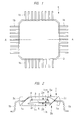
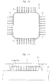
- FIG. 1 is a plan view showing one example of a structure of a semiconductor device of the present embodiment
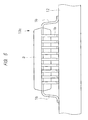
- FIG. 2 is a cross-sectional view showing one example of a structure taken along a line A-A of FIG. 1
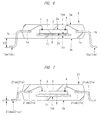
- FIG. 3 is an enlarged cross-sectional view showing the detailed structure of the semiconductor device shown in FIG. 1
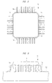
- FIG. 4 is a plan view showing one example of a mounting structure onto a mounting board of the semiconductor device of FIG. 1
- FIG. 5 is a side view showing one example of the mounting structure of the semiconductor device (QFP) shown in FIG. 4 .
- a mounting structure shown in FIG. 4 is a module (electronic device) 20 in which a plurality of semiconductor devices and electronic components are mounted on a motherboard 12 serving as a wiring board.
- a motherboard 12 serving as a wiring board.
- an in-vehicle motherboard (mounting board, hereinafter, referred to also as an ECU (Electronic Control Unit) board) 12 is taken as an example. Note that, in the present embodiment, in order to distinguish from electronic components such as capacitors and resistors, electronic components having semiconductor chips mounted therein are described as semiconductor devices.
- an ECU board for use in controlling an engine is jointed and fixed to an engine room by pins (bolts) made of metal. Therefore, heat generated in the engine room is conducted to the ECU board via the metal pins.
- the semiconductor devices and electronic components mounted on the ECU board for use in controlling an engine are used under a severe environment.
- various semiconductor devices such as QFPs 13a, 13b, 13c and 13d, SOPs (Small Outline Packages) 14a and 14b and others are mounted.
- various electronic components such as capacitors (chip tantalum capacitors 15, laminated ceramic capacitors 17 and aluminum electrolytic capacitors 18) and resistors (including chip resistors) 16 are also mounted thereon.
- capacitors chip tantalum capacitors 15, laminated ceramic capacitors 17 and aluminum electrolytic capacitors 18
- resistors including chip resistors
- a plurality of (for example, five) metal pins (bolts) 19 are inserted into the motherboard 12.
- the motherboard 12 constituting the module (electronic device) 20 is likely to be deformed (expanded, contracted, strained, deflected, or the like) in a part near each of the pins 19.
- semiconductor devices and electronic components disposed (mounted) near the pins 19 are present under an environment in which a mounting failure is likely to occur in comparison with the semiconductor devices and electronic components that are not disposed (mounted) near the pins 19.
- the semiconductor device of the present embodiment shown in FIG. 1 and FIG. 2 is a semiconductor package provided with a sealing body which seals a semiconductor chip and a plurality of leads which protrude from the sealing body.
- a QFP (Quad Flat Package) 5 in which a plurality of outer parts (external connection terminals) 1b protrude from a sealing body 3 made of resin and the respective outer parts 1b are bent into a gull-wing shape is taken as one example of the above-mentioned semiconductor device.
- the QFP 5 is a semiconductor device in which a plurality of outer parts 1b serving as external connection terminals protrude from two pairs of mutually opposed sides of the sealing body 3 having a substantially square shape in its planar shape.
- the structure of the QFP 5 will be described below.
- the QFP 5 is provided with a die pad (chip mounting portion, tab) 1c having an upper surface (chip mounting surface) 1ca and a lower surface 1cb opposite to the upper surface 1ca, a semiconductor chip 2 mounted on the die pad 1c, a plurality of leads disposed around the die pad 1c and the sealing body 3.
- the semiconductor chip 2 is provided with a main surface 2a, a plurality of bonding pads (bonding electrodes) 2c formed on the main surface 2a, and a back surface 2b opposite to the main surface 2a, and as shown in FIG. 2 , the semiconductor chip 2 is mounted on the upper surface 1ca of the die pad 1c via a die bond material 6 such that the back surface 2b faces the upper surface 1ca of the die pad 1c.
- a die bond material 6 for example, a paste adhesive such as an Ag paste is used, but a film adhesive may also be used.
- the die pad 1c is supported by a plurality of suspension leads (see FIG. 15 to be described later) 1e, and the plurality of leads that do not support the die pad 1c are electrically connected with the plurality of bonding pads 2c of the semiconductor chip 2 respectively via a plurality of wires 4.
- Each of the plurality of wires 4 is, for example, a gold wire, a copper wire, or the like.
- the sealing body 3 has an upper surface (front surface) 3a positioned on a main surface 2a side of the semiconductor chip 2, a lower surface (mounting surface) 3b opposite to the upper surface 3a, and side surfaces 3c located between the upper surface 3a and the lower surface 3b, and is made of sealing resin or the like.
- the lower surface 3b of the sealing body 3 corresponds to a surface located on a lower surface 1cb side of the die pad 1c.
- the sealing body 3 seals the die pad 1c, the other parts (inner parts) of the plurality of leads, the semiconductor chip 2 and the plurality of wires 4 such that one parts (outer parts) of the plurality of leads protrude from the side surfaces 3c.
- parts buried in the sealing body 3 correspond to inner parts 1a
- parts protruding externally from the side surfaces 3c of the sealing body 3 correspond to outer parts (one parts) 1b.
- the inner part 1a and the outer part 1b are integrally formed as one unit.
- each of the plurality of leads is bent on the outside of the sealing body 3. More specifically, each of the outer parts 1b of the plurality of leads is bent into a gull-wing shape.
- each of the plurality of leads has a surface coated with a plating film (metal film) 7 (except for a cut surface, see FIG. 29 to be described later).
- sealing body 3 is made of, for example, thermosetting epoxy-based resin.
- the semiconductor chip 2 is composed of, for example, a base material made of silicon and a multilayer wiring layer that is formed on an element formation surface of the base material and has a thickness smaller than that of the base material.
- the sealing body 3 is partially disposed above the main surface 2a of the semiconductor chip 2 and below the lower surface 1cb of the die pad 1c. More specifically, the QFP 5 is a semiconductor device having a so-called tab embedded structure in which the die pad 1c is buried in the sealing body 3.
- the thickness T1 of the semiconductor chip 2 is larger than the thickness T5 from the lower surface 1cb of the die pad 1c to the lower surface 3b of the sealing body 3 as shown in FIG. 3 .
- T1 is, for example, 0.4 mm
- T5 is, for example, 0.39 mm.
- the QFP 5 is a semiconductor device whose occupancy ratio of the semiconductor chip 2 inside the sealing body 3 is high.
- the occupancy ratio of the semiconductor chip 2 refers to a ratio (dominating amount) of the thickness of the semiconductor chip 2 relative to the total thickness of the sealing body 3 in the thickness direction of the sealing body 3. Therefore, as one example of a comparison target for the chip thickness, the thickness of the sealing body 3 below the chip is proposed.
- the thickness T5 of the sealing body 3 below the lower surface 1cb of the die pad 1c is smaller than the thickness T1 of the semiconductor chip 2.
- a distance D1 from the lower surface 3b of the sealing body 3 to each of the tip portions (main joint surfaces) 1be of the respective outer parts 1b of the plurality of leads is larger than a thickness T4 of the sealing body 3 from the main surface 2a of the semiconductor chip 2 to the upper surface 3a of the sealing body 3.
- D1 is, for example, 0.73 mm
- T4 is, for example, 0.47 mm.
- the above-mentioned distance D1 is a stand-off amount of the QFP 5 of the present embodiment.
- the stand-off amount of the QFP 5 is a distance from the lower surface 3b of the sealing body 3 to the lowermost point of the tip portion 1be of the outer part 1b.
- an average of three sides of bottommost points on a bottom surface 0.1 mm inner than the tip end of the outer part 1b is determined as a virtual plane by taking into account the scanner dimensional inspection, and this virtual plane is defined as the lowermost point.
- a surface (lower surface 1bb) facing the surface of the electrode pad (for example, terminal 12b of the motherboard 12 shown in FIG. 31 ) of the motherboard 12 on which the QFP 5 is mounted (solder-bonded) is defined as a main joint surface. More specifically, since the tip portion 1be of each outer part 1b corresponds to a surface on which a solder material wets up, all the surfaces (except for a cut surface) on which the above-mentioned plating film 7 is formed serve as joint surfaces, but since the surface (lower surface 1bb) facing the electrode pad of the mounting board mainly serves as a joint surface, this surface is defined as the main joint surface.
- each of the plurality of inner parts 1a of the QFP 5 has a wire joint portion 1ac to which the wire 4 is bonded and which is sealed with the sealing body 3.
- each of the plurality of outer parts 1b has a bending portion 1bc that is bent in the thickness direction of the sealing body 3 and a bending portion 1bd that is bent in a direction parallel with the upper surface 3a of the sealing body 3, so that the bending portion 1bc and the bending portion 1bd form a gull-wing shape.
- each of the bending portion 1bc and the bending portion 1bd is formed in the outer part 1b and thus exposed from the sealing body 3, and the bending portion 1bc is disposed so as to be spaced apart from the semiconductor chip 2 compared with the wire joint portion 1ac of the inner part 1a, while the bending portion 1bd is formed at a position spaced apart from the semiconductor chip 2 compared with the bending portion 1bc.
- a distance (gap, D1 (stand-off amount)) of each of the plurality of outer parts 1b from the lower surface 3b of the sealing body 3 to the bending portion 1bd is larger than a thickness T8 from the upper surface 1aa of each of the wire joint portions 1ac of the plurality of inner parts 1a to the upper surface 3a of the sealing body 3 or a thickness T9 from the lower surface 1 ⁇ ab of each of the wire joint portions 1ac of the plurality of inner parts 1a to the lower surface 3b of the sealing body 3.
- T8 and T9 are, for example, 0.64 mm, but T8 and T9 are not necessarily equal to each other.
- the distance (gap, D1 (stand-off amount)) from the lower surface 3b of the sealing body 3 to each of the tip portions 1be of the plurality of outer parts 1b is larger than the thickness of the semiconductor chip 2. More specifically, in the QFP 5, D1 > T1 is satisfied.
- FIG. 6 is a cross-sectional view showing the structure of the semiconductor device (QFP) of the present embodiment
- FIG. 7 is a cross-sectional view showing the structure of a QFP of a comparative example
- FIG. 8 is a plan view showing one example of the structure of the semiconductor device of the present embodiment
- FIG. 9 is a side view showing the mounting structure of the semiconductor device shown in FIG. 8
- FIG. 10 is a plan view showing the structure of the QFP of the comparative example
- FIG. 11 is a side view showing the mounting structure of the semiconductor device shown in FIG. 10 .
- the QFP 5 of the present embodiment is a semiconductor device having a large stand-off amount (D1).
- the thicknesses of the sealing bodies of the QFP, LQPF and TQFP based on JEITA are 2.00 mm, 1.40 mm and 1.00 mm, respectively.
- the stand-off amounts (for example, d1 of QFP 21 shown in FIG. 7 ) of all the QFP, LQPF and TQFP based on JEITA are 0.10 mm in the low-stand value and 0.40 mm in the high-stand value.
- the QFP 5 of the present embodiment has a structure based on JEITA and the thickness of the sealing body 3 corresponds to that of the LQFP of JEITA, while the length of each outer part 1b (in particular, the length in the thickness direction of the sealing body 3) is made longer, so that the stand-off amount is larger than the stand-off amount (in particular, the high-stand value) of each of the QFP, LQFP and TQFP based on JEITA.
- the distance (gap) between the sealing body 3 and the motherboard 12 is larger in the QFP 5 of the present embodiment as shown in FIG. 8 to FIG. 11 .
- the QFP 21 shown in FIG. 7 has the same structure as that of the LQFP based on JEITA, and with respect to a plurality of leads 21a each made up of an inner part 21aa and an outer part 21ab, the stand-off amount d1 corresponding to a distance between a lower surface 21aba of the tip portion 21ac of the outer part 21ab and the lower surface 3b of the sealing body 3 is smaller than the thickness of the semiconductor chip 2 and a distance between the lower surface 1cb of the die pad 1c and the lower surface 3b of the sealing body 3.
- the stand-off amount d1 of the QFP 21 is extremely small.
- the above-mentioned numerical values are given by way of example and various modifications may be made.
- the QFP 5 of the present embodiment is a semiconductor device in which the reduction in thickness of the sealing body 3 is achieved.
- the QFP 5 of the present embodiment is a semiconductor device in which the occupancy ratio of the semiconductor chip 2 inside the sealing body 3 tends to be high, so that rigidity of the semiconductor device main body is also high.
- the planar shape of the sealing body 3 is a square shape with one side of about 5 to 6 mm
- the planar shape of the semiconductor chip 2 is a rectangular shape or a square shape with one side of about 2 to 2.5 mm.
- the QFP 5 having such a high occupancy ratio of the semiconductor chip 2 inside the sealing body 3 is mounted on a wiring board such as the motherboard 12 or the like, if the board is warped due to an influence of heat or the like, the movement of the QFP 5 hardly follows the warping of the board because the rigidity of the QFP main body (sealing body 3) is high.
- the movement of the main body (sealing body 3) is made to easily follow the warping of the board.
- the thermal expansion coefficient includes a linear expansion coefficient that is an index of the expansion rate in a linear direction and a volume expansion coefficient that is an index of the expansion rate in a three-dimensional space, and as a cause of occurrence of a stress due to a temperature cycle load, the difference in the linear expansion coefficient gives great influences.
- the semiconductor chip 2 is mainly made of silicon and the linear expansion coefficient thereof is 4 to 5 ppm/°C, and the sealing body 3 (resin) is mainly made of epoxy resin and the linear expansion coefficient thereof is 8 to 12 ppm/°C. Therefore, the linear expansion coefficient of the semiconductor chip 2 is smaller than the linear expansion coefficient of the sealing body 3.
- the lead frame 1 (see FIG. 14 to be described later) including the die pad 1c is mainly made of a copper (Cu) material and the linear expansion coefficient thereof is 17 ppm/°C.
- the motherboard 12 on which the QFP 5 is mounted is mainly made of a resin material and the linear expansion coefficient thereof is, for example, about 15 ppm/°C.
- the linear expansion coefficient of the semiconductor chip 2 is smaller than the linear expansion coefficient of the sealing body 3, the linear expansion coefficient of the QFP 5 itself is lowered when the occupancy ratio of the semiconductor chip 2 inside the sealing body 3 is increased, so that the rigidity of the QFP main body (sealing body 3) becomes higher as described above.
- the sealing body 3 of the QFP 5 is made of thermosetting epoxy-based resin, while the semiconductor chip 2 is formed of a base material made of silicon and a multilayer wiring layer (having insulating layers between respective wiring layers) that is formed on an element formation surface of the base material and thinner than the base material. For this reason, the linear expansion coefficient of the semiconductor chip 2 (4 to 5 ppm) is smaller than the linear expansion coefficient of the sealing body 3 (8 to 12 ppm) .
- the thickness of the semiconductor chip 2 (LQFP: 0.40 mm, TQFP: 0.28 mm) is larger than the thickness of the sealing body 3 from the lower surface 1cb of the die pad 1c to the lower surface 3b of the sealing body 3 (LQFP: 0.38 mm, TQFP: 0.23 mm).
- the whole thickness of the sealing body 3 tends to become smaller. Consequently, with the reduction of the whole thickness of the sealing body 3, the thickness of the sealing body 3 located below the die pad 1c becomes smaller than the thickness of the semiconductor chip 2. As a result, the occupancy ratio of the semiconductor chip 2 inside the sealing body 3 is increased, so that the linear expansion coefficient of the semiconductor device itself is decreased (the rigidity of the semiconductor device main body (sealing body 3) is increased).
- the QFP 5 of the present embodiment since the stand-off amount of each of the plurality of outer parts 1b is large, the movement of the QFP 5 main body (sealing body 3) is allowed to easily follow the warping of the motherboard 12.
- FIG. 12 is a diagram showing a solder wet-up state in the QFP 5 of the present embodiment. As shown in FIG. 12 , since the stand-off amount of each outer part 1b is large in the QFP 5, the wet-up of the solder 8 in each outer part 1b is increased in the height direction of each of the outer parts 1b.
- the strength of the solder bonding is enhanced between each of the outer parts 1b and the joint portion. Moreover, since the movement of the QFP 5 main body (sealing body 3) is allowed to easily follow the warping of the motherboard 12 as described above, it is possible to ensure high mounting reliability (mounting strength) in the QFP 5.
- an ECU board for use in controlling an engine is jointed and fixed to an engine room by pins (bolts) made of metal. Therefore, since heat generated in the engine room is conducted to the ECU board via the metal pins, the semiconductor devices and electronic components mounted on the ECU board for use in controlling an engine are used under a severe environment.
- the motherboard (for example, ECU board) 12 on which semiconductor devices are mounted is fixed to the engine room by a plurality of pins (bolts) 19. Since the respective pins 19 are made of metal, the temperature of the pins 19 is easily raised when the operating environment thereof is exposed to a high temperature.
- the motherboard 12 tends to be easily warped (strained) in the vicinity of the respective pins 19 in comparison with other regions (regions spaced apart from the pins 19).
- the joint failure is likely to occur in the semiconductor devices disposed (mounted) in the vicinity of the pins 19 in comparison with the semiconductor devices disposed in the other regions.
- QFPs 13b and 13c have two pins 19 disposed adjacent thereto. Therefore, by adopting the structure having a large stand-off amount of the present embodiment to these QFPs 13b and 13c, it is possible to enhance the mounting reliability (mounting strength) even in the QFPs 13b and 13c that tend to be subjected to the thermal influence. As a result, it becomes possible to reduce the joint failure to the motherboard 12 (ECU board).
- the structure of the present embodiment having a large stand-off amount may be applied also to a semiconductor device disposed in a region spaced apart from the pins 19.
- the structure of the present embodiment having a large stand-off amount may be applied to the QFP 13a and QFP 13d or SOP 14a and SOP 14b. In this manner, the mounting reliability (mounting strength) of these semiconductor devices can be further improved.
- FIG. 13 is a conceptual diagram showing a solder wet-up state in the semiconductor device of the comparative example.
- the QFP 21 shown in FIG. 13 has a structure in which each of the outer parts 21ab is extended long in the direction of the mounting surface of the board.
- the wet-up amount of the solder 8 is smaller than that of the QFP 5 of the present embodiment, it is not possible to sufficiently enhance the mounting reliability (mounting strength).
- the wet-up of the solder 8 since the wet-up of the solder 8 has directionality, the wet-up of the solder 8 stops at the bending portion of the outer part 21ab in the case of the QFP 21 of FIG. 13 . Therefore, it is not possible to ensure the sufficient mounting reliability (mounting strength) equivalent to that of the QFP 5 of the present embodiment, and failing to withstand the use in such a severe environment as that of the motherboard 12 (ECU board) of the module 20 shown in FIG. 4 .
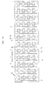
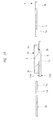
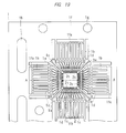
- FIG. 14 is a plan view showing a structure of a lead frame for use in the assembling of the semiconductor device of FIG. 1
- FIG. 15 is a partially enlarged plan view showing the structure of a part A of FIG. 14 in an enlarged manner
- FIG. 16 is a cross-sectional view showing a cross-sectional structure taken along a line A-A of FIG. 15
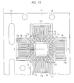
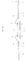
- FIG. 17 is a partially enlarged plan view showing a structure after die bonding in the assembling of the semiconductor device of FIG. 1
- FIG. 18 is a cross-sectional view showing a cross-sectional structure taken along a line A-A of FIG. 17 .
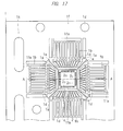
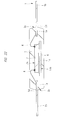
- FIG. 19 is a partially enlarged plan view showing a structure after wire bonding in the assembling of the semiconductor device of FIG. 1
- FIG. 20 is a cross-sectional view showing a cross-sectional structure taken along a line A-A of FIG. 19
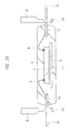
- FIG. 21 is a partially enlarged plan view showing a structure after resin molding in the assembling of the semiconductor device of FIG. 1
- FIG. 22 is a cross-sectional view showing a cross-sectional structure taken along a line A-A of FIG. 21 .
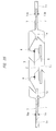
- FIG. 23 is a cross-sectional view showing a structure at the time of cutting a dam in the assembling of the semiconductor device of FIG. 1
- FIG. 24 is a cross-sectional view showing one example of a structure at the time of laser marking in the assembling of the semiconductor device of FIG. 1
- FIG. 25 is a cross-sectional view showing one example of a structure after external plating formation in the assembling of the semiconductor device of FIG. 1
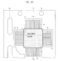
- FIG. 26 is a partially enlarged plan view showing one example of a structure after gate-tip cutting in the assembling of the semiconductor device of FIG. 1 .
- FIG. 27 is a partially enlarged plan view showing one example of a structure after lead cutting and shaping in the assembling of the semiconductor device of FIG. 1
- FIG. 28 is a plan view showing one example of a structure after corner portion cutting in the assembling of the semiconductor device of FIG. 1
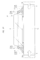
- FIG. 29 is a cross-sectional view showing the structure of FIG. 28
- FIG. 30 is an external perspective view of the structure of FIG. 28 .
- a thin plate-shaped lead frame 1 in which a plurality of device regions (device formation portions) 1i are formed inside a frame portion If as shown in FIG. 14 is prepared.
- the device region 1i is a region in which one QFP 5 is formed.
- the plurality of device regions 1i are disposed in a matrix pattern when seen in a plan view, but these may be disposed in one row (single row) and the number of the device regions 1i to be formed on one lead frame 1 is not particularly limited.
- the planar shape of the lead frame is a rectangular shape.
- a plurality of holes 1g for use in positioning, guiding or the like are formed along a pair of sides (short sides) mutually opposed to each other of the frame portions If of the lead frame 1, a plurality of holes 1g for use in positioning, guiding or the like are formed. Furthermore, between the mutually adjacent device regions of the plurality of device regions 1i, a plurality of elongated holes 1h are formed along a pair of sides (short sides) mutually opposed to each other.
- one die pad 1c is formed in one device region 1i.
- the planar shape of the die pad in the present embodiment is a substantially square shape.
- the four corners of the die pad 1c are supported by suspension leads 1e.
- a plurality of leads are formed around the die pad 1c.
- Each lead is made up of an inner part 1a and an outer part 1b connected thereto.
- an end portion of each outer part 1b is connected with an inner frame 1fa formed on the inside (die pad side) of the frame portion If.
- the mutually adjacent outer parts are coupled to each other by a dam bar 1d at a position slightly outside the border portion between the inner part 1a and the outer part 1b.
- each of the plurality of outer parts 1b is formed into an elongated shape such that the stand-off amount of the lead formed in the subsequent lead shaping process becomes large.
- the die pad 1c supported by the suspension leads 1e is disposed at a position lower than the plurality of inner parts 1a. More specifically, a bent portion is formed in the middle of each suspension lead 1e, whereby the die pad 1c is located at a position lower than the plurality of inner parts 1a.
- the lead frame 1 is made of, for example, a metal material mainly made of copper.
- one device region 1i is taken as a representative example for the following description of the assembling of the QFP 5.
- the semiconductor chip 2 is mounted on the upper surface 1ca of the die pad 1c via the die bond material 6. More specifically, the semiconductor chip 2 having a plurality of bonding pads 2c formed on the main surface 2a thereof is mounted on the die pad 1c via the die bond material 6.
- wire bonding is carried out.
- the plurality of bonding pads 2c of the semiconductor chip 2 and the plurality of inner parts 1a are electrically connected with one another via a plurality of wires 4. At this time, each of the one ends of the plurality of wires 4 is bonded to each of wire joint portions 1ac of the plurality of inner parts 1a.
- the semiconductor chip 2, the die pad 1c, the plurality of inner parts 1a and the plurality of wires 4 are sealed by using sealing resin.
- the lead frame 1 that has been subjected to the wire bonding is disposed in a cavity of a resin molding die (not shown) and the lead frame 1 is clamped by the molding die, and then the sealing resin is injected into the cavity, thereby forming the sealing body 3.
- the above-mentioned sealing resin is, for example, thermosetting epoxy resin, and the sealing body 3 is formed by a thermosetting process after the injection process.
- a gate resin 22 shown in FIG. 21 is formed at one of the corner portions of the sealing body 3 seen in a plan view.
- the structure shown in FIG. 22 in which a plurality of outer parts 1b protrude from the respective side surfaces 3c of the sealing body 3 is formed.
- lead cutting (dam bar cutting) is carried out.
- a dam bar 1d disposed between the adjacent outer parts is cut by a cutting blade 9. Note that, in the dam bar cutting process, only the cutting of the dam bar 1d is carried out.
- the upper surface 3a of the sealing body 3 is irradiated with a laser 10, and marks 11 such as a predetermined production number, a management number and the like are applied on the upper surface 3a of the sealing body 3 as shown in FIG. 26 to be described later.
- plating film formation is carried out.
- a plating film (external plating) 7 such as solder plating or the like is formed on the respective surfaces (surfaces including the upper surface 1ba and the lower surface 1bb) of the plurality of outer parts 1b.
- solder plating When solder plating is used as the plating film 7, it is preferable to adopt lead-free solder, and by adopting the lead-free solder, it is possible to reduce the environmental load.
- the lead-free solder mentioned here refers to the solder having a content of lead (Pb) of 0.1 wt% or less, and this content is determined based on a standard of RoHS (Restriction of Hazardous Substance) directive.
- the inner frame 1fa that connects tip ends of the respective outer parts 1b with each other is cut off from the frame portion If (see FIG. 26 ).
- the outer parts 1b are shaped (bent) into, for example, a gull-wing shape as shown in FIG. 29 .
- the inner frame 1fa that connects the tip ends of the respective outer parts 1b with each other is cut, thereby separating the respective outer parts 1b from each other (see FIG. 27 ).
- lead cutting (corner portion cutting) is carried out.
- the QFP 5 is mounted on the motherboard 12 serving as the mounting board via the solder 8 as shown in FIG. 12 .
- the wet-up amount of the solder 8 is increased in each of the outer parts 1b, so that the solder 8 wets up to a high position (to the bending portion 1bc shown in FIG. 3 ) in the height direction of each of the outer parts 1b.
- the QFP 5 is a semiconductor device having a high occupancy ratio of the semiconductor chip 2 inside the sealing body 3, and even in the case of the QFP 5 having such a high occupancy ratio of the semiconductor chip 2, it is possible to enhance the mounting reliability and consequently to reduce the joint failure to the motherboard 12.
- the QFP has a die-pad embedded structure
- the QFP may have a so-called tab exposed structure in which a part (for example, lower surface 1cb) of the die pad 1c is exposed from the sealing body 3.
- the semiconductor device is the QFP
- the semiconductor device may be a semiconductor device of a so-called SOP (Small Outline Package) type in which a plurality of leads serving as external connection terminals protrude from two mutually opposed sides of the sealing body 3 having a substantially square shape in its planar shape.
- SOP Small Outline Package
- the occupancy ratio of the semiconductor chip 2 corresponds to the ratio (dominating amount) of the thickness of the semiconductor chip 2 relative to the total thickness of the sealing body 3 in the thickness direction of the sealing body 3.
- the comparison target for the chip thickness is not limited to the thickness of the sealing body 3 below the die pad, and the thickness of the sealing body 3 above the chip may be adopted thereto.
- the thickness of the sealing body 3 formed above (on the main surface side) of the semiconductor chip 2 is larger than the thickness of the semiconductor chip 2 in most cases so as to prevent the wires 4 from being exposed to the surface of the sealing body 3. Therefore, when determining the occupancy ratio (dominating amount) of the semiconductor chip 2 in the sealing body 3, the thickness of the sealing body 3 below the die pad is preferably adopted as the comparison target.
- each of the plurality of outer parts 1b in the semiconductor device QFP 5
- each of the plurality of outer parts 1b may have a J-lead shape.
- the semiconductor device may be a QFJ (Quad Flat J-leaded Package) or an SOJ (Small Outline J-leaded Package).
- the external plating application process after the molding process can be omitted.
- the plating film 7 formed on each of the outer parts 1b in the external plating process is a plating film made of a solder material, and the solder material is a lead-free solder substantially containing no lead (Pb) has been described, but the solder material may be a material containing lead.
- the solder material may be a material containing lead.
- the use of a solder material made of lead-free solder is more preferable.
Landscapes
- Structures Or Materials For Encapsulating Or Coating Semiconductor Devices Or Solid State Devices (AREA)
- Lead Frames For Integrated Circuits (AREA)
- Wire Bonding (AREA)
Applications Claiming Priority (1)
| Application Number | Priority Date | Filing Date | Title |
|---|---|---|---|
| JP2014050460A JP2015176907A (ja) | 2014-03-13 | 2014-03-13 | 半導体装置 |
Publications (2)
| Publication Number | Publication Date |
|---|---|
| EP2927953A2 true EP2927953A2 (de) | 2015-10-07 |
| EP2927953A3 EP2927953A3 (de) | 2015-11-25 |
Family
ID=51904832
Family Applications (1)
| Application Number | Title | Priority Date | Filing Date |
|---|---|---|---|
| EP14194103.9A Withdrawn EP2927953A3 (de) | 2014-03-13 | 2014-11-20 | Halbleiterbauelement |
Country Status (6)
| Country | Link |
|---|---|
| US (3) | US10032700B2 (de) |
| EP (1) | EP2927953A3 (de) |
| JP (1) | JP2015176907A (de) |
| KR (1) | KR20150107574A (de) |
| CN (3) | CN110931438B (de) |
| TW (2) | TW201834173A (de) |
Families Citing this family (9)
| Publication number | Priority date | Publication date | Assignee | Title |
|---|---|---|---|---|
| JP2015176907A (ja) | 2014-03-13 | 2015-10-05 | ルネサスエレクトロニクス株式会社 | 半導体装置 |
| JPWO2017002268A1 (ja) * | 2015-07-02 | 2017-10-19 | ルネサスエレクトロニクス株式会社 | 半導体装置の製造方法および半導体装置 |
| US9728508B2 (en) | 2015-09-18 | 2017-08-08 | Taiwan Semiconductor Manufacturing Company, Ltd. | Semiconductor device and method of manufacture |
| JP2017135230A (ja) * | 2016-01-27 | 2017-08-03 | ルネサスエレクトロニクス株式会社 | 半導体装置およびその製造方法 |
| JP6629914B2 (ja) * | 2018-05-01 | 2020-01-15 | ルネサスエレクトロニクス株式会社 | 半導体装置 |
| JP2019197796A (ja) | 2018-05-09 | 2019-11-14 | ルネサスエレクトロニクス株式会社 | 半導体装置の製造方法 |
| US10777489B2 (en) | 2018-05-29 | 2020-09-15 | Katoh Electric Co., Ltd. | Semiconductor module |
| CN110914981B (zh) * | 2018-05-29 | 2023-06-16 | 新电元工业株式会社 | 半导体模块 |
| CN109003947A (zh) * | 2018-07-23 | 2018-12-14 | 苏州锝耀电子有限公司 | 大功率层叠式芯片结构 |
Citations (2)
| Publication number | Priority date | Publication date | Assignee | Title |
|---|---|---|---|---|
| JPH053277A (ja) | 1991-06-25 | 1993-01-08 | Hitachi Ltd | 半導体装置 |
| JP2004319954A (ja) | 2003-04-04 | 2004-11-11 | Nikon Corp | 表面実装型部品及びその製造に用いるリードフレーム |
Family Cites Families (29)
| Publication number | Priority date | Publication date | Assignee | Title |
|---|---|---|---|---|
| KR960006710B1 (ko) * | 1987-02-25 | 1996-05-22 | 가부시기가이샤 히다찌세이사꾸쇼 | 면실장형 반도체집적회로장치 및 그 제조방법과 그 실장방법 |
| JP2873009B2 (ja) * | 1988-09-20 | 1999-03-24 | 株式会社日立製作所 | 半導体装置およびその製造方法 |
| US5041901A (en) * | 1989-05-10 | 1991-08-20 | Hitachi, Ltd. | Lead frame and semiconductor device using the same |
| JPH0423460A (ja) * | 1990-05-18 | 1992-01-27 | Mitsubishi Electric Corp | 半導体装置 |
| JPH0494747U (de) * | 1991-01-17 | 1992-08-17 | ||
| JPH04320359A (ja) * | 1991-04-19 | 1992-11-11 | Hitachi Ltd | 半導体装置 |
| JPH0590473A (ja) * | 1991-09-27 | 1993-04-09 | Hitachi Ltd | 半導体装置 |
| JP3075617B2 (ja) * | 1991-12-25 | 2000-08-14 | 株式会社日立製作所 | 半導体集積回路装置 |
| JPH05198722A (ja) * | 1992-01-21 | 1993-08-06 | Mitsubishi Electric Corp | 半導体装置 |
| JPH07263610A (ja) | 1994-03-18 | 1995-10-13 | Fujitsu Ltd | 表面実装型半導体装置及びプリント配線板 |
| WO1996009645A1 (en) * | 1994-09-20 | 1996-03-28 | Hitachi, Ltd. | Semiconductor device and its mounting structure |
| JPH08222681A (ja) * | 1995-02-14 | 1996-08-30 | Toshiba Corp | 樹脂封止型半導体装置 |
| US5841190A (en) * | 1995-05-19 | 1998-11-24 | Ibiden Co., Ltd. | High density multi-layered printed wiring board, multi-chip carrier and semiconductor package |
| JP3954585B2 (ja) * | 1998-10-14 | 2007-08-08 | 株式会社ルネサステクノロジ | 半導体装置 |
| JP4206177B2 (ja) * | 1998-10-21 | 2009-01-07 | 株式会社ルネサステクノロジ | 半導体装置 |
| JP2001274316A (ja) * | 2000-03-23 | 2001-10-05 | Hitachi Ltd | 半導体装置及びその製造方法 |
| JP3497847B2 (ja) * | 2001-08-23 | 2004-02-16 | 沖電気工業株式会社 | 半導体装置およびその製造方法 |
| JP2004228259A (ja) * | 2003-01-22 | 2004-08-12 | Hitachi Ltd | 半導体装置及びそれを用いた電子装置 |
| JP2007129182A (ja) * | 2005-05-11 | 2007-05-24 | Toshiba Corp | 半導体装置 |
| JP5089184B2 (ja) * | 2007-01-30 | 2012-12-05 | ローム株式会社 | 樹脂封止型半導体装置およびその製造方法 |
| JP2009099905A (ja) * | 2007-10-19 | 2009-05-07 | Rohm Co Ltd | 半導体装置 |
| WO2011007570A1 (ja) * | 2009-07-17 | 2011-01-20 | パナソニック株式会社 | 電子モジュールおよびその製造方法 |
| JP2012084795A (ja) | 2010-10-14 | 2012-04-26 | Mitsubishi Electric Corp | 実装部品仮固定用接着剤の供給方法、半導体装置の製造方法、部品実装用基板および半導体装置 |
| JP5830718B2 (ja) * | 2011-05-02 | 2015-12-09 | パナソニックIpマネジメント株式会社 | 熱硬化性樹脂組成物、プリプレグ、積層板、金属箔張積層板、及び回路基板 |
| TWI569381B (zh) * | 2011-05-27 | 2017-02-01 | 住友電木股份有限公司 | 半導體裝置 |
| JP2013243263A (ja) * | 2012-05-21 | 2013-12-05 | Internatl Business Mach Corp <Ibm> | 3次元積層パッケージにおける電力供給と放熱(冷却)との両立 |
| JP6030970B2 (ja) * | 2013-02-12 | 2016-11-24 | エスアイアイ・セミコンダクタ株式会社 | 樹脂封止型半導体装置およびその製造方法 |
| JP5767294B2 (ja) * | 2013-10-07 | 2015-08-19 | ルネサスエレクトロニクス株式会社 | 半導体装置 |
| JP2015176907A (ja) | 2014-03-13 | 2015-10-05 | ルネサスエレクトロニクス株式会社 | 半導体装置 |
-
2014
- 2014-03-13 JP JP2014050460A patent/JP2015176907A/ja active Pending
- 2014-11-06 KR KR1020140153625A patent/KR20150107574A/ko not_active Withdrawn
- 2014-11-13 TW TW107122021A patent/TW201834173A/zh unknown
- 2014-11-13 TW TW103139425A patent/TW201535650A/zh unknown
- 2014-11-18 CN CN201911240957.2A patent/CN110931438B/zh active Active
- 2014-11-18 CN CN201410658551.7A patent/CN104916618B/zh active Active
- 2014-11-18 CN CN201420692867.3U patent/CN204204846U/zh not_active Expired - Fee Related
- 2014-11-20 EP EP14194103.9A patent/EP2927953A3/de not_active Withdrawn
-
2015
- 2015-01-09 US US14/593,689 patent/US10032700B2/en active Active
-
2018
- 2018-06-26 US US16/019,301 patent/US10461020B2/en active Active
-
2019
- 2019-09-20 US US16/577,596 patent/US10796983B2/en active Active
Patent Citations (2)
| Publication number | Priority date | Publication date | Assignee | Title |
|---|---|---|---|---|
| JPH053277A (ja) | 1991-06-25 | 1993-01-08 | Hitachi Ltd | 半導体装置 |
| JP2004319954A (ja) | 2003-04-04 | 2004-11-11 | Nikon Corp | 表面実装型部品及びその製造に用いるリードフレーム |
Also Published As
| Publication number | Publication date |
|---|---|
| KR20150107574A (ko) | 2015-09-23 |
| CN110931438A (zh) | 2020-03-27 |
| US20150262922A1 (en) | 2015-09-17 |
| US20200013702A1 (en) | 2020-01-09 |
| EP2927953A3 (de) | 2015-11-25 |
| CN104916618B (zh) | 2019-12-31 |
| US20180315686A1 (en) | 2018-11-01 |
| US10461020B2 (en) | 2019-10-29 |
| TW201834173A (zh) | 2018-09-16 |
| US10796983B2 (en) | 2020-10-06 |
| CN104916618A (zh) | 2015-09-16 |
| JP2015176907A (ja) | 2015-10-05 |
| CN110931438B (zh) | 2025-02-25 |
| TW201535650A (zh) | 2015-09-16 |
| US10032700B2 (en) | 2018-07-24 |
| CN204204846U (zh) | 2015-03-11 |
Similar Documents
| Publication | Publication Date | Title |
|---|---|---|
| US10796983B2 (en) | Positional relationship among components of semiconductor device | |
| US20160056097A1 (en) | Semiconductor device with inspectable solder joints | |
| EP3001453A1 (de) | Halbleiterbauelement | |
| CN101553920B (zh) | 方型扁平无引线封装及其方法 | |
| US9013030B2 (en) | Leadframe, semiconductor package including a leadframe and method for producing a leadframe | |
| US9184142B2 (en) | Semiconductor device and manufacturing method of the same | |
| US20050110127A1 (en) | Semiconductor device | |
| KR20170092112A (ko) | 수지 봉지형 반도체 장치 | |
| US12074098B2 (en) | Three-dimensional functional integration | |
| US6078099A (en) | Lead frame structure for preventing the warping of semiconductor package body | |
| JP5034670B2 (ja) | モールドパッケージ | |
| CN108074901B (zh) | 具有可湿拐角引线的半导体器件及半导体器件组装方法 | |
| CN1334603A (zh) | 集成电路的平面化塑料封装模块 | |
| CN107204299A (zh) | 半导体装置的制造方法及半导体装置 | |
| CN112956005B (zh) | 包含向内弯曲引线的集成电路封装 | |
| JP6629914B2 (ja) | 半導体装置 | |
| JPH06216492A (ja) | 電子装置 | |
| KR200235610Y1 (ko) | 적층형반도체패키지 | |
| CN119890173A (zh) | 混合四方扁平封装电子装置 | |
| JPH0737917A (ja) | 電子部品及びそのモジュール構造 | |
| JPH05283574A (ja) | 樹脂モールド型半導体装置 |
Legal Events
| Date | Code | Title | Description |
|---|---|---|---|
| PUAI | Public reference made under article 153(3) epc to a published international application that has entered the european phase |
Free format text: ORIGINAL CODE: 0009012 |
|
| AK | Designated contracting states |
Kind code of ref document: A2 Designated state(s): AL AT BE BG CH CY CZ DE DK EE ES FI FR GB GR HR HU IE IS IT LI LT LU LV MC MK MT NL NO PL PT RO RS SE SI SK SM TR |
|
| AX | Request for extension of the european patent |
Extension state: BA ME |
|
| PUAL | Search report despatched |
Free format text: ORIGINAL CODE: 0009013 |
|
| RAP1 | Party data changed (applicant data changed or rights of an application transferred) |
Owner name: RENESAS ELECTRONICS CORPORATION |
|
| AK | Designated contracting states |
Kind code of ref document: A3 Designated state(s): AL AT BE BG CH CY CZ DE DK EE ES FI FR GB GR HR HU IE IS IT LI LT LU LV MC MK MT NL NO PL PT RO RS SE SI SK SM TR |
|
| AX | Request for extension of the european patent |
Extension state: BA ME |
|
| RIC1 | Information provided on ipc code assigned before grant |
Ipc: H01L 23/31 20060101AFI20151020BHEP Ipc: H01L 23/495 20060101ALI20151020BHEP |
|
| 17P | Request for examination filed |
Effective date: 20160525 |
|
| RBV | Designated contracting states (corrected) |
Designated state(s): AL AT BE BG CH CY CZ DE DK EE ES FI FR GB GR HR HU IE IS IT LI LT LU LV MC MK MT NL NO PL PT RO RS SE SI SK SM TR |
|
| 17Q | First examination report despatched |
Effective date: 20161012 |
|
| RIC1 | Information provided on ipc code assigned before grant |
Ipc: H01L 23/31 20060101ALI20190315BHEP Ipc: H01L 23/544 20060101ALI20190315BHEP Ipc: H01L 23/495 20060101ALI20190315BHEP Ipc: H01L 21/48 20060101AFI20190315BHEP |
|
| GRAP | Despatch of communication of intention to grant a patent |
Free format text: ORIGINAL CODE: EPIDOSNIGR1 |
|
| INTG | Intention to grant announced |
Effective date: 20190426 |
|
| STAA | Information on the status of an ep patent application or granted ep patent |
Free format text: STATUS: THE APPLICATION IS DEEMED TO BE WITHDRAWN |
|
| 18D | Application deemed to be withdrawn |
Effective date: 20190907 |