EP2960689A1 - Miroir réfléchissant de collecte de lumière solaire - Google Patents
Miroir réfléchissant de collecte de lumière solaire Download PDFInfo
- Publication number
- EP2960689A1 EP2960689A1 EP14754171.8A EP14754171A EP2960689A1 EP 2960689 A1 EP2960689 A1 EP 2960689A1 EP 14754171 A EP14754171 A EP 14754171A EP 2960689 A1 EP2960689 A1 EP 2960689A1
- Authority
- EP
- European Patent Office
- Prior art keywords
- support member
- group
- mirror
- film
- film mirror
- Prior art date
- Legal status (The legal status is an assumption and is not a legal conclusion. Google has not performed a legal analysis and makes no representation as to the accuracy of the status listed.)
- Granted
Links
- 230000002093 peripheral effect Effects 0.000 claims abstract description 12
- 229920005989 resin Polymers 0.000 claims description 75
- 239000011347 resin Substances 0.000 claims description 75
- 239000000758 substrate Substances 0.000 claims description 66
- 230000005855 radiation Effects 0.000 claims description 39
- 238000002310 reflectometry Methods 0.000 abstract description 19
- 239000010408 film Substances 0.000 description 164
- 239000010410 layer Substances 0.000 description 149
- XAGFODPZIPBFFR-UHFFFAOYSA-N aluminium Chemical compound [Al] XAGFODPZIPBFFR-UHFFFAOYSA-N 0.000 description 60
- 238000000034 method Methods 0.000 description 53
- 238000007772 electroless plating Methods 0.000 description 40
- 229910052782 aluminium Inorganic materials 0.000 description 36
- 239000003054 catalyst Substances 0.000 description 36
- 238000007747 plating Methods 0.000 description 35
- 229910052751 metal Inorganic materials 0.000 description 28
- 239000002184 metal Substances 0.000 description 28
- 239000004925 Acrylic resin Substances 0.000 description 27
- 229920000178 Acrylic resin Polymers 0.000 description 22
- 239000000243 solution Substances 0.000 description 22
- 229920000642 polymer Polymers 0.000 description 21
- 239000004820 Pressure-sensitive adhesive Substances 0.000 description 20
- 239000002243 precursor Substances 0.000 description 19
- XEKOWRVHYACXOJ-UHFFFAOYSA-N Ethyl acetate Chemical compound CCOC(C)=O XEKOWRVHYACXOJ-UHFFFAOYSA-N 0.000 description 18
- 239000000463 material Substances 0.000 description 18
- 229920000139 polyethylene terephthalate Polymers 0.000 description 16
- 239000005020 polyethylene terephthalate Substances 0.000 description 16
- 229910052709 silver Inorganic materials 0.000 description 16
- 229910021645 metal ion Inorganic materials 0.000 description 15
- XLYOFNOQVPJJNP-UHFFFAOYSA-N water Substances O XLYOFNOQVPJJNP-UHFFFAOYSA-N 0.000 description 13
- 239000012018 catalyst precursor Substances 0.000 description 12
- 238000006243 chemical reaction Methods 0.000 description 12
- 238000009713 electroplating Methods 0.000 description 12
- 125000000524 functional group Chemical group 0.000 description 11
- -1 polyethylene Polymers 0.000 description 11
- 239000000470 constituent Substances 0.000 description 10
- 230000002452 interceptive effect Effects 0.000 description 10
- 150000002500 ions Chemical class 0.000 description 10
- 238000011282 treatment Methods 0.000 description 10
- 239000004332 silver Substances 0.000 description 9
- WSFSSNUMVMOOMR-UHFFFAOYSA-N Formaldehyde Chemical compound O=C WSFSSNUMVMOOMR-UHFFFAOYSA-N 0.000 description 8
- BQCADISMDOOEFD-UHFFFAOYSA-N Silver Chemical compound [Ag] BQCADISMDOOEFD-UHFFFAOYSA-N 0.000 description 8
- 230000015572 biosynthetic process Effects 0.000 description 8
- 239000003638 chemical reducing agent Substances 0.000 description 8
- 230000000052 comparative effect Effects 0.000 description 8
- 239000010949 copper Substances 0.000 description 8
- 238000010438 heat treatment Methods 0.000 description 8
- 239000000203 mixture Substances 0.000 description 8
- PXHVJJICTQNCMI-UHFFFAOYSA-N nickel Substances [Ni] PXHVJJICTQNCMI-UHFFFAOYSA-N 0.000 description 8
- 239000012790 adhesive layer Substances 0.000 description 7
- 239000007864 aqueous solution Substances 0.000 description 7
- 125000004435 hydrogen atom Chemical group [H]* 0.000 description 7
- 125000005647 linker group Chemical group 0.000 description 7
- 125000002496 methyl group Chemical group [H]C([H])([H])* 0.000 description 7
- 150000003839 salts Chemical class 0.000 description 7
- 239000000126 substance Substances 0.000 description 7
- VYPSYNLAJGMNEJ-UHFFFAOYSA-N Silicium dioxide Chemical compound O=[Si]=O VYPSYNLAJGMNEJ-UHFFFAOYSA-N 0.000 description 6
- HEMHJVSKTPXQMS-UHFFFAOYSA-M Sodium hydroxide Chemical compound [OH-].[Na+] HEMHJVSKTPXQMS-UHFFFAOYSA-M 0.000 description 6
- GWEVSGVZZGPLCZ-UHFFFAOYSA-N Titan oxide Chemical compound O=[Ti]=O GWEVSGVZZGPLCZ-UHFFFAOYSA-N 0.000 description 6
- 229920001577 copolymer Polymers 0.000 description 6
- 229920000058 polyacrylate Polymers 0.000 description 6
- 125000000217 alkyl group Chemical group 0.000 description 5
- 125000002843 carboxylic acid group Chemical group 0.000 description 5
- 229910052802 copper Inorganic materials 0.000 description 5
- 230000007547 defect Effects 0.000 description 5
- 238000011156 evaluation Methods 0.000 description 5
- 238000004519 manufacturing process Methods 0.000 description 5
- 229910052759 nickel Inorganic materials 0.000 description 5
- 229910052763 palladium Inorganic materials 0.000 description 5
- 238000006722 reduction reaction Methods 0.000 description 5
- 239000002904 solvent Substances 0.000 description 5
- HRPVXLWXLXDGHG-UHFFFAOYSA-N Acrylamide Chemical group NC(=O)C=C HRPVXLWXLXDGHG-UHFFFAOYSA-N 0.000 description 4
- WKBOTKDWSSQWDR-UHFFFAOYSA-N Bromine atom Chemical compound [Br] WKBOTKDWSSQWDR-UHFFFAOYSA-N 0.000 description 4
- JOYRKODLDBILNP-UHFFFAOYSA-N Ethyl urethane Chemical compound CCOC(N)=O JOYRKODLDBILNP-UHFFFAOYSA-N 0.000 description 4
- CSNNHWWHGAXBCP-UHFFFAOYSA-L Magnesium sulfate Chemical compound [Mg+2].[O-][S+2]([O-])([O-])[O-] CSNNHWWHGAXBCP-UHFFFAOYSA-L 0.000 description 4
- UIIMBOGNXHQVGW-UHFFFAOYSA-M Sodium bicarbonate Chemical compound [Na+].OC([O-])=O UIIMBOGNXHQVGW-UHFFFAOYSA-M 0.000 description 4
- 230000003197 catalytic effect Effects 0.000 description 4
- 238000000576 coating method Methods 0.000 description 4
- 125000004093 cyano group Chemical group *C#N 0.000 description 4
- 239000012153 distilled water Substances 0.000 description 4
- 239000011521 glass Substances 0.000 description 4
- 125000002887 hydroxy group Chemical group [H]O* 0.000 description 4
- 150000002739 metals Chemical class 0.000 description 4
- FQPSGWSUVKBHSU-UHFFFAOYSA-N methacrylamide Chemical group CC(=C)C(N)=O FQPSGWSUVKBHSU-UHFFFAOYSA-N 0.000 description 4
- 229920001225 polyester resin Polymers 0.000 description 4
- 239000004645 polyester resin Substances 0.000 description 4
- SQGYOTSLMSWVJD-UHFFFAOYSA-N silver(1+) nitrate Chemical compound [Ag+].[O-]N(=O)=O SQGYOTSLMSWVJD-UHFFFAOYSA-N 0.000 description 4
- 239000010935 stainless steel Substances 0.000 description 4
- 229910001220 stainless steel Inorganic materials 0.000 description 4
- 125000000547 substituted alkyl group Chemical group 0.000 description 4
- FXHOOIRPVKKKFG-UHFFFAOYSA-N N,N-Dimethylacetamide Chemical compound CN(C)C(C)=O FXHOOIRPVKKKFG-UHFFFAOYSA-N 0.000 description 3
- 239000004734 Polyphenylene sulfide Substances 0.000 description 3
- KWYUFKZDYYNOTN-UHFFFAOYSA-M Potassium hydroxide Chemical compound [OH-].[K+] KWYUFKZDYYNOTN-UHFFFAOYSA-M 0.000 description 3
- JUJWROOIHBZHMG-UHFFFAOYSA-N Pyridine Chemical group C1=CC=NC=C1 JUJWROOIHBZHMG-UHFFFAOYSA-N 0.000 description 3
- 125000003647 acryloyl group Chemical group O=C([*])C([H])=C([H])[H] 0.000 description 3
- 230000003213 activating effect Effects 0.000 description 3
- 239000000853 adhesive Substances 0.000 description 3
- 230000001070 adhesive effect Effects 0.000 description 3
- 239000003513 alkali Substances 0.000 description 3
- 239000011248 coating agent Substances 0.000 description 3
- 229910052681 coesite Inorganic materials 0.000 description 3
- 229910052906 cristobalite Inorganic materials 0.000 description 3
- 239000006185 dispersion Substances 0.000 description 3
- 125000001033 ether group Chemical group 0.000 description 3
- 125000001495 ethyl group Chemical group [H]C([H])([H])C([H])([H])* 0.000 description 3
- 229910052742 iron Inorganic materials 0.000 description 3
- 239000007769 metal material Substances 0.000 description 3
- KDLHZDBZIXYQEI-UHFFFAOYSA-N palladium Substances [Pd] KDLHZDBZIXYQEI-UHFFFAOYSA-N 0.000 description 3
- 229920006122 polyamide resin Polymers 0.000 description 3
- 229920000069 polyphenylene sulfide Polymers 0.000 description 3
- 230000009467 reduction Effects 0.000 description 3
- 239000000377 silicon dioxide Substances 0.000 description 3
- 239000010944 silver (metal) Substances 0.000 description 3
- 238000004544 sputter deposition Methods 0.000 description 3
- 229910052682 stishovite Inorganic materials 0.000 description 3
- 125000001273 sulfonato group Chemical group [O-]S(*)(=O)=O 0.000 description 3
- 229910052905 tridymite Inorganic materials 0.000 description 3
- JYEUMXHLPRZUAT-UHFFFAOYSA-N 1,2,3-triazine Chemical group C1=CN=NN=C1 JYEUMXHLPRZUAT-UHFFFAOYSA-N 0.000 description 2
- ARXJGSRGQADJSQ-UHFFFAOYSA-N 1-methoxypropan-2-ol Chemical compound COCC(C)O ARXJGSRGQADJSQ-UHFFFAOYSA-N 0.000 description 2
- HZAXFHJVJLSVMW-UHFFFAOYSA-N 2-Aminoethan-1-ol Chemical compound NCCO HZAXFHJVJLSVMW-UHFFFAOYSA-N 0.000 description 2
- RYKLZUPYJFFNRR-UHFFFAOYSA-N 3-hydroxypiperidin-2-one Chemical compound OC1CCCNC1=O RYKLZUPYJFFNRR-UHFFFAOYSA-N 0.000 description 2
- IJGRMHOSHXDMSA-UHFFFAOYSA-N Atomic nitrogen Chemical compound N#N IJGRMHOSHXDMSA-UHFFFAOYSA-N 0.000 description 2
- AFVFQIVMOAPDHO-UHFFFAOYSA-N Methanesulfonic acid Chemical compound CS(O)(=O)=O AFVFQIVMOAPDHO-UHFFFAOYSA-N 0.000 description 2
- 239000004696 Poly ether ether ketone Substances 0.000 description 2
- 239000004695 Polyether sulfone Substances 0.000 description 2
- 239000004698 Polyethylene Substances 0.000 description 2
- CDBYLPFSWZWCQE-UHFFFAOYSA-L Sodium Carbonate Chemical compound [Na+].[Na+].[O-]C([O-])=O CDBYLPFSWZWCQE-UHFFFAOYSA-L 0.000 description 2
- PPBRXRYQALVLMV-UHFFFAOYSA-N Styrene Chemical compound C=CC1=CC=CC=C1 PPBRXRYQALVLMV-UHFFFAOYSA-N 0.000 description 2
- 239000002390 adhesive tape Substances 0.000 description 2
- 125000003368 amide group Chemical group 0.000 description 2
- 125000004429 atom Chemical group 0.000 description 2
- 125000000484 butyl group Chemical group [H]C([*])([H])C([H])([H])C([H])([H])C([H])([H])[H] 0.000 description 2
- 125000003178 carboxy group Chemical group [H]OC(*)=O 0.000 description 2
- 229910052801 chlorine Inorganic materials 0.000 description 2
- 229910052804 chromium Inorganic materials 0.000 description 2
- 239000011651 chromium Substances 0.000 description 2
- XLJMAIOERFSOGZ-UHFFFAOYSA-M cyanate group Chemical group [O-]C#N XLJMAIOERFSOGZ-UHFFFAOYSA-M 0.000 description 2
- 125000004185 ester group Chemical group 0.000 description 2
- 229910052737 gold Inorganic materials 0.000 description 2
- 239000010931 gold Substances 0.000 description 2
- 125000005843 halogen group Chemical group 0.000 description 2
- 230000006872 improvement Effects 0.000 description 2
- 239000003999 initiator Substances 0.000 description 2
- 239000011133 lead Substances 0.000 description 2
- 229910052943 magnesium sulfate Inorganic materials 0.000 description 2
- 235000019341 magnesium sulphate Nutrition 0.000 description 2
- 239000011259 mixed solution Substances 0.000 description 2
- 239000000178 monomer Substances 0.000 description 2
- 229920006287 phenoxy resin Polymers 0.000 description 2
- 239000013034 phenoxy resin Substances 0.000 description 2
- 125000000843 phenylene group Chemical group C1(=C(C=CC=C1)*)* 0.000 description 2
- 125000002467 phosphate group Chemical group [H]OP(=O)(O[H])O[*] 0.000 description 2
- 229920003229 poly(methyl methacrylate) Polymers 0.000 description 2
- 229920006393 polyether sulfone Polymers 0.000 description 2
- 229920002530 polyetherether ketone Polymers 0.000 description 2
- 229920000573 polyethylene Polymers 0.000 description 2
- 229920001721 polyimide Polymers 0.000 description 2
- 239000009719 polyimide resin Substances 0.000 description 2
- 239000004926 polymethyl methacrylate Substances 0.000 description 2
- 230000008569 process Effects 0.000 description 2
- 125000001436 propyl group Chemical group [H]C([*])([H])C([H])([H])C([H])([H])[H] 0.000 description 2
- 230000009257 reactivity Effects 0.000 description 2
- 229910001961 silver nitrate Inorganic materials 0.000 description 2
- NSVHDIYWJVLAGH-UHFFFAOYSA-M silver;n,n-diethylcarbamodithioate Chemical compound [Ag+].CCN(CC)C([S-])=S NSVHDIYWJVLAGH-UHFFFAOYSA-M 0.000 description 2
- 235000017557 sodium bicarbonate Nutrition 0.000 description 2
- 229910000030 sodium bicarbonate Inorganic materials 0.000 description 2
- 235000011121 sodium hydroxide Nutrition 0.000 description 2
- 239000007787 solid Substances 0.000 description 2
- 238000001179 sorption measurement Methods 0.000 description 2
- 239000007858 starting material Substances 0.000 description 2
- 125000005504 styryl group Chemical group 0.000 description 2
- 238000003786 synthesis reaction Methods 0.000 description 2
- 229920002803 thermoplastic polyurethane Polymers 0.000 description 2
- 229910052718 tin Inorganic materials 0.000 description 2
- 239000011135 tin Substances 0.000 description 2
- 125000000391 vinyl group Chemical group [H]C([*])=C([H])[H] 0.000 description 2
- 229910052725 zinc Inorganic materials 0.000 description 2
- 239000011701 zinc Substances 0.000 description 2
- QNODIIQQMGDSEF-UHFFFAOYSA-N (1-hydroxycyclohexyl)-phenylmethanone Chemical compound C=1C=CC=CC=1C(=O)C1(O)CCCCC1 QNODIIQQMGDSEF-UHFFFAOYSA-N 0.000 description 1
- ZXSQEZNORDWBGZ-UHFFFAOYSA-N 1,3-dihydropyrrolo[2,3-b]pyridin-2-one Chemical compound C1=CN=C2NC(=O)CC2=C1 ZXSQEZNORDWBGZ-UHFFFAOYSA-N 0.000 description 1
- XQUPVDVFXZDTLT-UHFFFAOYSA-N 1-[4-[[4-(2,5-dioxopyrrol-1-yl)phenyl]methyl]phenyl]pyrrole-2,5-dione Chemical compound O=C1C=CC(=O)N1C(C=C1)=CC=C1CC1=CC=C(N2C(C=CC2=O)=O)C=C1 XQUPVDVFXZDTLT-UHFFFAOYSA-N 0.000 description 1
- HAZJTCQWIDBCCE-UHFFFAOYSA-N 1h-triazine-6-thione Chemical group SC1=CC=NN=N1 HAZJTCQWIDBCCE-UHFFFAOYSA-N 0.000 description 1
- SMZOUWXMTYCWNB-UHFFFAOYSA-N 2-(2-methoxy-5-methylphenyl)ethanamine Chemical compound COC1=CC=C(C)C=C1CCN SMZOUWXMTYCWNB-UHFFFAOYSA-N 0.000 description 1
- NIXOWILDQLNWCW-UHFFFAOYSA-N 2-Propenoic acid Natural products OC(=O)C=C NIXOWILDQLNWCW-UHFFFAOYSA-N 0.000 description 1
- YOCIJWAHRAJQFT-UHFFFAOYSA-N 2-bromo-2-methylpropanoyl bromide Chemical compound CC(C)(Br)C(Br)=O YOCIJWAHRAJQFT-UHFFFAOYSA-N 0.000 description 1
- UZFMOKQJFYMBGY-UHFFFAOYSA-N 4-hydroxy-TEMPO Chemical compound CC1(C)CC(O)CC(C)(C)N1[O] UZFMOKQJFYMBGY-UHFFFAOYSA-N 0.000 description 1
- NLHHRLWOUZZQLW-UHFFFAOYSA-N Acrylonitrile Chemical compound C=CC#N NLHHRLWOUZZQLW-UHFFFAOYSA-N 0.000 description 1
- 229910000838 Al alloy Inorganic materials 0.000 description 1
- VHUUQVKOLVNVRT-UHFFFAOYSA-N Ammonium hydroxide Chemical compound [NH4+].[OH-] VHUUQVKOLVNVRT-UHFFFAOYSA-N 0.000 description 1
- ZOXJGFHDIHLPTG-UHFFFAOYSA-N Boron Chemical compound [B] ZOXJGFHDIHLPTG-UHFFFAOYSA-N 0.000 description 1
- OKTJSMMVPCPJKN-UHFFFAOYSA-N Carbon Chemical compound [C] OKTJSMMVPCPJKN-UHFFFAOYSA-N 0.000 description 1
- 239000004215 Carbon black (E152) Substances 0.000 description 1
- ZAMOUSCENKQFHK-UHFFFAOYSA-N Chlorine atom Chemical compound [Cl] ZAMOUSCENKQFHK-UHFFFAOYSA-N 0.000 description 1
- VYZAMTAEIAYCRO-UHFFFAOYSA-N Chromium Chemical compound [Cr] VYZAMTAEIAYCRO-UHFFFAOYSA-N 0.000 description 1
- RYGMFSIKBFXOCR-UHFFFAOYSA-N Copper Chemical compound [Cu] RYGMFSIKBFXOCR-UHFFFAOYSA-N 0.000 description 1
- 229920000089 Cyclic olefin copolymer Polymers 0.000 description 1
- 239000004641 Diallyl-phthalate Substances 0.000 description 1
- 239000004593 Epoxy Substances 0.000 description 1
- 229910013720 M(NO3)n Inorganic materials 0.000 description 1
- 239000004640 Melamine resin Substances 0.000 description 1
- 229920000877 Melamine resin Polymers 0.000 description 1
- 125000000815 N-oxide group Chemical group 0.000 description 1
- 229910019142 PO4 Inorganic materials 0.000 description 1
- OAICVXFJPJFONN-UHFFFAOYSA-N Phosphorus Chemical compound [P] OAICVXFJPJFONN-UHFFFAOYSA-N 0.000 description 1
- 239000004743 Polypropylene Substances 0.000 description 1
- 229920000297 Rayon Polymers 0.000 description 1
- 229910021607 Silver chloride Inorganic materials 0.000 description 1
- NINIDFKCEFEMDL-UHFFFAOYSA-N Sulfur Chemical compound [S] NINIDFKCEFEMDL-UHFFFAOYSA-N 0.000 description 1
- LSNNMFCWUKXFEE-UHFFFAOYSA-N Sulfurous acid Chemical group OS(O)=O LSNNMFCWUKXFEE-UHFFFAOYSA-N 0.000 description 1
- UCKMPCXJQFINFW-UHFFFAOYSA-N Sulphide Chemical compound [S-2] UCKMPCXJQFINFW-UHFFFAOYSA-N 0.000 description 1
- YTPLMLYBLZKORZ-UHFFFAOYSA-N Thiophene Chemical group C=1C=CSC=1 YTPLMLYBLZKORZ-UHFFFAOYSA-N 0.000 description 1
- ATJFFYVFTNAWJD-UHFFFAOYSA-N Tin Chemical compound [Sn] ATJFFYVFTNAWJD-UHFFFAOYSA-N 0.000 description 1
- RTAQQCXQSZGOHL-UHFFFAOYSA-N Titanium Chemical compound [Ti] RTAQQCXQSZGOHL-UHFFFAOYSA-N 0.000 description 1
- 229920001807 Urea-formaldehyde Polymers 0.000 description 1
- WYGWHHGCAGTUCH-ISLYRVAYSA-N V-65 Substances CC(C)CC(C)(C#N)\N=N\C(C)(C#N)CC(C)C WYGWHHGCAGTUCH-ISLYRVAYSA-N 0.000 description 1
- BZHJMEDXRYGGRV-UHFFFAOYSA-N Vinyl chloride Chemical compound ClC=C BZHJMEDXRYGGRV-UHFFFAOYSA-N 0.000 description 1
- 229920002433 Vinyl chloride-vinyl acetate copolymer Polymers 0.000 description 1
- HCHKCACWOHOZIP-UHFFFAOYSA-N Zinc Chemical compound [Zn] HCHKCACWOHOZIP-UHFFFAOYSA-N 0.000 description 1
- VYGUBTIWNBFFMQ-UHFFFAOYSA-N [N+](#[C-])N1C(=O)NC=2NC(=O)NC2C1=O Chemical group [N+](#[C-])N1C(=O)NC=2NC(=O)NC2C1=O VYGUBTIWNBFFMQ-UHFFFAOYSA-N 0.000 description 1
- HFBMWMNUJJDEQZ-UHFFFAOYSA-N acryloyl chloride Chemical compound ClC(=O)C=C HFBMWMNUJJDEQZ-UHFFFAOYSA-N 0.000 description 1
- 125000001931 aliphatic group Chemical group 0.000 description 1
- 150000003973 alkyl amines Chemical group 0.000 description 1
- 125000002947 alkylene group Chemical group 0.000 description 1
- 125000006365 alkylene oxy carbonyl group Chemical group 0.000 description 1
- 125000005529 alkyleneoxy group Chemical group 0.000 description 1
- 125000000320 amidine group Chemical group 0.000 description 1
- 125000003277 amino group Chemical group 0.000 description 1
- QGZKDVFQNNGYKY-UHFFFAOYSA-O ammonium group Chemical group [NH4+] QGZKDVFQNNGYKY-UHFFFAOYSA-O 0.000 description 1
- 235000011114 ammonium hydroxide Nutrition 0.000 description 1
- 125000002490 anilino group Chemical group [H]N(*)C1=C([H])C([H])=C([H])C([H])=C1[H] 0.000 description 1
- 150000001450 anions Chemical class 0.000 description 1
- 229910052787 antimony Inorganic materials 0.000 description 1
- 125000002029 aromatic hydrocarbon group Chemical group 0.000 description 1
- QVGXLLKOCUKJST-UHFFFAOYSA-N atomic oxygen Chemical compound [O] QVGXLLKOCUKJST-UHFFFAOYSA-N 0.000 description 1
- 125000000852 azido group Chemical group *N=[N+]=[N-] 0.000 description 1
- 125000000751 azo group Chemical group [*]N=N[*] 0.000 description 1
- 239000002585 base Substances 0.000 description 1
- 125000003785 benzimidazolyl group Chemical group N1=C(NC2=C1C=CC=C2)* 0.000 description 1
- IOJUPLGTWVMSFF-UHFFFAOYSA-N benzothiazole Chemical group C1=CC=C2SC=NC2=C1 IOJUPLGTWVMSFF-UHFFFAOYSA-N 0.000 description 1
- 125000003354 benzotriazolyl group Chemical group N1N=NC2=C1C=CC=C2* 0.000 description 1
- QUDWYFHPNIMBFC-UHFFFAOYSA-N bis(prop-2-enyl) benzene-1,2-dicarboxylate Chemical compound C=CCOC(=O)C1=CC=CC=C1C(=O)OCC=C QUDWYFHPNIMBFC-UHFFFAOYSA-N 0.000 description 1
- 229910052797 bismuth Inorganic materials 0.000 description 1
- 229910052796 boron Inorganic materials 0.000 description 1
- RJTANRZEWTUVMA-UHFFFAOYSA-N boron;n-methylmethanamine Chemical compound [B].CNC RJTANRZEWTUVMA-UHFFFAOYSA-N 0.000 description 1
- 125000005620 boronic acid group Chemical group 0.000 description 1
- GDTBXPJZTBHREO-UHFFFAOYSA-N bromine Substances BrBr GDTBXPJZTBHREO-UHFFFAOYSA-N 0.000 description 1
- 229910052794 bromium Inorganic materials 0.000 description 1
- 229910052799 carbon Inorganic materials 0.000 description 1
- 239000004918 carbon fiber reinforced polymer Substances 0.000 description 1
- 125000005587 carbonate group Chemical group 0.000 description 1
- 125000002915 carbonyl group Chemical group [*:2]C([*:1])=O 0.000 description 1
- 230000015556 catabolic process Effects 0.000 description 1
- 238000010531 catalytic reduction reaction Methods 0.000 description 1
- 229920002301 cellulose acetate Polymers 0.000 description 1
- 239000012461 cellulose resin Substances 0.000 description 1
- 239000000919 ceramic Substances 0.000 description 1
- 239000000460 chlorine Substances 0.000 description 1
- 125000001309 chloro group Chemical group Cl* 0.000 description 1
- 238000004140 cleaning Methods 0.000 description 1
- 238000004440 column chromatography Methods 0.000 description 1
- 238000010276 construction Methods 0.000 description 1
- 238000007796 conventional method Methods 0.000 description 1
- 238000004132 cross linking Methods 0.000 description 1
- LDHQCZJRKDOVOX-NSCUHMNNSA-N crotonic acid Chemical group C\C=C\C(O)=O LDHQCZJRKDOVOX-NSCUHMNNSA-N 0.000 description 1
- 230000001186 cumulative effect Effects 0.000 description 1
- 238000006731 degradation reaction Methods 0.000 description 1
- 238000000151 deposition Methods 0.000 description 1
- 238000011161 development Methods 0.000 description 1
- 238000010586 diagram Methods 0.000 description 1
- 125000000664 diazo group Chemical group [N-]=[N+]=[*] 0.000 description 1
- 238000007607 die coating method Methods 0.000 description 1
- OJKANDGLELGDHV-UHFFFAOYSA-N disilver;dioxido(dioxo)chromium Chemical compound [Ag+].[Ag+].[O-][Cr]([O-])(=O)=O OJKANDGLELGDHV-UHFFFAOYSA-N 0.000 description 1
- 239000002612 dispersion medium Substances 0.000 description 1
- 239000000428 dust Substances 0.000 description 1
- 230000000694 effects Effects 0.000 description 1
- 238000010894 electron beam technology Methods 0.000 description 1
- 239000003822 epoxy resin Substances 0.000 description 1
- UHESRSKEBRADOO-UHFFFAOYSA-N ethyl carbamate;prop-2-enoic acid Chemical compound OC(=O)C=C.CCOC(N)=O UHESRSKEBRADOO-UHFFFAOYSA-N 0.000 description 1
- 125000000816 ethylene group Chemical group [H]C([H])([*:1])C([H])([H])[*:2] 0.000 description 1
- 229910052731 fluorine Inorganic materials 0.000 description 1
- 125000001153 fluoro group Chemical group F* 0.000 description 1
- 239000007849 furan resin Substances 0.000 description 1
- 229910052733 gallium Inorganic materials 0.000 description 1
- 229910052732 germanium Inorganic materials 0.000 description 1
- PCHJSUWPFVWCPO-UHFFFAOYSA-N gold Chemical compound [Au] PCHJSUWPFVWCPO-UHFFFAOYSA-N 0.000 description 1
- 238000007756 gravure coating Methods 0.000 description 1
- 229930195733 hydrocarbon Natural products 0.000 description 1
- 150000002430 hydrocarbons Chemical group 0.000 description 1
- RCCPEORTSYDPMB-UHFFFAOYSA-N hydroxy benzenecarboximidothioate Chemical group OSC(=N)C1=CC=CC=C1 RCCPEORTSYDPMB-UHFFFAOYSA-N 0.000 description 1
- 125000002883 imidazolyl group Chemical group 0.000 description 1
- 125000005462 imide group Chemical group 0.000 description 1
- 238000007654 immersion Methods 0.000 description 1
- 229910052738 indium Inorganic materials 0.000 description 1
- 238000007733 ion plating Methods 0.000 description 1
- 238000010884 ion-beam technique Methods 0.000 description 1
- 229910052741 iridium Inorganic materials 0.000 description 1
- LDHQCZJRKDOVOX-IHWYPQMZSA-N isocrotonic acid Chemical group C\C=C/C(O)=O LDHQCZJRKDOVOX-IHWYPQMZSA-N 0.000 description 1
- LVHBHZANLOWSRM-UHFFFAOYSA-N itaconic acid Chemical group OC(=O)CC(=C)C(O)=O LVHBHZANLOWSRM-UHFFFAOYSA-N 0.000 description 1
- 229910052745 lead Inorganic materials 0.000 description 1
- VZCYOOQTPOCHFL-UPHRSURJSA-N maleic acid Chemical group OC(=O)\C=C/C(O)=O VZCYOOQTPOCHFL-UPHRSURJSA-N 0.000 description 1
- 229910052748 manganese Inorganic materials 0.000 description 1
- 230000007246 mechanism Effects 0.000 description 1
- QSHDDOUJBYECFT-UHFFFAOYSA-N mercury Chemical compound [Hg] QSHDDOUJBYECFT-UHFFFAOYSA-N 0.000 description 1
- 229910052753 mercury Inorganic materials 0.000 description 1
- 229910001507 metal halide Inorganic materials 0.000 description 1
- 150000005309 metal halides Chemical class 0.000 description 1
- 229940098779 methanesulfonic acid Drugs 0.000 description 1
- 125000000956 methoxy group Chemical group [H]C([H])([H])O* 0.000 description 1
- 125000001570 methylene group Chemical group [H]C([H])([*:1])[*:2] 0.000 description 1
- 125000000449 nitro group Chemical group [O-][N+](*)=O 0.000 description 1
- 229910052757 nitrogen Inorganic materials 0.000 description 1
- QJGQUHMNIGDVPM-UHFFFAOYSA-N nitrogen group Chemical group [N] QJGQUHMNIGDVPM-UHFFFAOYSA-N 0.000 description 1
- 125000000018 nitroso group Chemical group N(=O)* 0.000 description 1
- 125000000962 organic group Chemical group 0.000 description 1
- 229910052760 oxygen Inorganic materials 0.000 description 1
- 239000001301 oxygen Substances 0.000 description 1
- 239000003002 pH adjusting agent Substances 0.000 description 1
- ISWSIDIOOBJBQZ-UHFFFAOYSA-N phenol group Chemical group C1(=CC=CC=C1)O ISWSIDIOOBJBQZ-UHFFFAOYSA-N 0.000 description 1
- 239000005011 phenolic resin Substances 0.000 description 1
- XYFCBTPGUUZFHI-UHFFFAOYSA-N phosphine group Chemical group P XYFCBTPGUUZFHI-UHFFFAOYSA-N 0.000 description 1
- ACVYVLVWPXVTIT-UHFFFAOYSA-N phosphinic acid Chemical compound O[PH2]=O ACVYVLVWPXVTIT-UHFFFAOYSA-N 0.000 description 1
- 125000002270 phosphoric acid ester group Chemical group 0.000 description 1
- 229910052698 phosphorus Inorganic materials 0.000 description 1
- 239000011574 phosphorus Substances 0.000 description 1
- 238000005240 physical vapour deposition Methods 0.000 description 1
- 125000004193 piperazinyl group Chemical group 0.000 description 1
- 125000003386 piperidinyl group Chemical group 0.000 description 1
- 239000002985 plastic film Substances 0.000 description 1
- 229920006255 plastic film Polymers 0.000 description 1
- 229910052697 platinum Inorganic materials 0.000 description 1
- BASFCYQUMIYNBI-UHFFFAOYSA-N platinum Substances [Pt] BASFCYQUMIYNBI-UHFFFAOYSA-N 0.000 description 1
- 229920003192 poly(bis maleimide) Polymers 0.000 description 1
- 229920003207 poly(ethylene-2,6-naphthalate) Polymers 0.000 description 1
- 229920002492 poly(sulfone) Polymers 0.000 description 1
- 229920005668 polycarbonate resin Polymers 0.000 description 1
- 239000004431 polycarbonate resin Substances 0.000 description 1
- 229920000647 polyepoxide Polymers 0.000 description 1
- 229920000728 polyester Polymers 0.000 description 1
- 239000011112 polyethylene naphthalate Substances 0.000 description 1
- 239000002952 polymeric resin Substances 0.000 description 1
- 238000006116 polymerization reaction Methods 0.000 description 1
- 229920005672 polyolefin resin Polymers 0.000 description 1
- 229920001955 polyphenylene ether Polymers 0.000 description 1
- 229920012287 polyphenylene sulfone Polymers 0.000 description 1
- 229920001155 polypropylene Polymers 0.000 description 1
- 229920001296 polysiloxane Polymers 0.000 description 1
- 239000004800 polyvinyl chloride Substances 0.000 description 1
- 229920000915 polyvinyl chloride Polymers 0.000 description 1
- 238000003825 pressing Methods 0.000 description 1
- 125000004805 propylene group Chemical group [H]C([H])([H])C([H])([*:1])C([H])([H])[*:2] 0.000 description 1
- 125000000561 purinyl group Chemical group N1=C(N=C2N=CNC2=C1)* 0.000 description 1
- 125000003373 pyrazinyl group Chemical group 0.000 description 1
- 125000003226 pyrazolyl group Chemical group 0.000 description 1
- UMJSCPRVCHMLSP-UHFFFAOYSA-N pyridine Natural products COC1=CC=CN=C1 UMJSCPRVCHMLSP-UHFFFAOYSA-N 0.000 description 1
- 125000000714 pyrimidinyl group Chemical group 0.000 description 1
- 125000000719 pyrrolidinyl group Chemical group 0.000 description 1
- 125000002294 quinazolinyl group Chemical group N1=C(N=CC2=CC=CC=C12)* 0.000 description 1
- 125000002943 quinolinyl group Chemical group N1=C(C=CC2=CC=CC=C12)* 0.000 description 1
- 125000001567 quinoxalinyl group Chemical group N1=C(C=NC2=CC=CC=C12)* 0.000 description 1
- 238000010526 radical polymerization reaction Methods 0.000 description 1
- 230000002285 radioactive effect Effects 0.000 description 1
- 238000001226 reprecipitation Methods 0.000 description 1
- 238000011160 research Methods 0.000 description 1
- 230000004044 response Effects 0.000 description 1
- 229910052703 rhodium Inorganic materials 0.000 description 1
- 229910052707 ruthenium Inorganic materials 0.000 description 1
- 229920002050 silicone resin Polymers 0.000 description 1
- NBYLLBXLDOPANK-UHFFFAOYSA-M silver 2-carboxyphenolate hydrate Chemical compound C1=CC=C(C(=C1)C(=O)O)[O-].O.[Ag+] NBYLLBXLDOPANK-UHFFFAOYSA-M 0.000 description 1
- CQLFBEKRDQMJLZ-UHFFFAOYSA-M silver acetate Chemical compound [Ag+].CC([O-])=O CQLFBEKRDQMJLZ-UHFFFAOYSA-M 0.000 description 1
- 229940071536 silver acetate Drugs 0.000 description 1
- ADZWSOLPGZMUMY-UHFFFAOYSA-M silver bromide Chemical compound [Ag]Br ADZWSOLPGZMUMY-UHFFFAOYSA-M 0.000 description 1
- 229910001958 silver carbonate Inorganic materials 0.000 description 1
- LKZMBDSASOBTPN-UHFFFAOYSA-L silver carbonate Substances [Ag].[O-]C([O-])=O LKZMBDSASOBTPN-UHFFFAOYSA-L 0.000 description 1
- 229940100890 silver compound Drugs 0.000 description 1
- 150000003379 silver compounds Chemical class 0.000 description 1
- LFAGQMCIGQNPJG-UHFFFAOYSA-N silver cyanide Chemical compound [Ag+].N#[C-] LFAGQMCIGQNPJG-UHFFFAOYSA-N 0.000 description 1
- 229940098221 silver cyanide Drugs 0.000 description 1
- HKZLPVFGJNLROG-UHFFFAOYSA-M silver monochloride Chemical compound [Cl-].[Ag+] HKZLPVFGJNLROG-UHFFFAOYSA-M 0.000 description 1
- YPNVIBVEFVRZPJ-UHFFFAOYSA-L silver sulfate Chemical compound [Ag+].[Ag+].[O-]S([O-])(=O)=O YPNVIBVEFVRZPJ-UHFFFAOYSA-L 0.000 description 1
- 229910000367 silver sulfate Inorganic materials 0.000 description 1
- RHUVFRWZKMEWNS-UHFFFAOYSA-M silver thiocyanate Chemical compound [Ag+].[S-]C#N RHUVFRWZKMEWNS-UHFFFAOYSA-M 0.000 description 1
- JUDUFOKGIZUSFP-UHFFFAOYSA-M silver;4-methylbenzenesulfonate Chemical compound [Ag+].CC1=CC=C(S([O-])(=O)=O)C=C1 JUDUFOKGIZUSFP-UHFFFAOYSA-M 0.000 description 1
- 239000012279 sodium borohydride Substances 0.000 description 1
- 229910000033 sodium borohydride Inorganic materials 0.000 description 1
- 229910000029 sodium carbonate Inorganic materials 0.000 description 1
- 235000017550 sodium carbonate Nutrition 0.000 description 1
- 238000004528 spin coating Methods 0.000 description 1
- 238000003756 stirring Methods 0.000 description 1
- 125000001174 sulfone group Chemical group 0.000 description 1
- 125000002130 sulfonic acid ester group Chemical group 0.000 description 1
- 125000003375 sulfoxide group Chemical group 0.000 description 1
- 125000005555 sulfoximide group Chemical group 0.000 description 1
- 229910052717 sulfur Inorganic materials 0.000 description 1
- 239000011593 sulfur Substances 0.000 description 1
- 230000001629 suppression Effects 0.000 description 1
- 230000002194 synthesizing effect Effects 0.000 description 1
- 125000001302 tertiary amino group Chemical group 0.000 description 1
- 229910052716 thallium Inorganic materials 0.000 description 1
- 229920005992 thermoplastic resin Polymers 0.000 description 1
- 239000010409 thin film Substances 0.000 description 1
- 125000000101 thioether group Chemical group 0.000 description 1
- 125000003396 thiol group Chemical group [H]S* 0.000 description 1
- UMGDCJDMYOKAJW-UHFFFAOYSA-N thiourea group Chemical group NC(=S)N UMGDCJDMYOKAJW-UHFFFAOYSA-N 0.000 description 1
- 229910052719 titanium Inorganic materials 0.000 description 1
- 239000010936 titanium Substances 0.000 description 1
- 125000001425 triazolyl group Chemical group 0.000 description 1
- XSQUKJJJFZCRTK-UHFFFAOYSA-N urea group Chemical group NC(=O)N XSQUKJJJFZCRTK-UHFFFAOYSA-N 0.000 description 1
- 238000007738 vacuum evaporation Methods 0.000 description 1
- 229910052720 vanadium Inorganic materials 0.000 description 1
- 238000007740 vapor deposition Methods 0.000 description 1
- 229910052724 xenon Inorganic materials 0.000 description 1
- FHNFHKCVQCLJFQ-UHFFFAOYSA-N xenon atom Chemical compound [Xe] FHNFHKCVQCLJFQ-UHFFFAOYSA-N 0.000 description 1
Images


Classifications
-
- F—MECHANICAL ENGINEERING; LIGHTING; HEATING; WEAPONS; BLASTING
- F24—HEATING; RANGES; VENTILATING
- F24S—SOLAR HEAT COLLECTORS; SOLAR HEAT SYSTEMS
- F24S25/00—Arrangement of stationary mountings or supports for solar heat collector modules
- F24S25/20—Peripheral frames for modules
-
- G—PHYSICS
- G02—OPTICS
- G02B—OPTICAL ELEMENTS, SYSTEMS OR APPARATUS
- G02B7/00—Mountings, adjusting means, or light-tight connections, for optical elements
- G02B7/18—Mountings, adjusting means, or light-tight connections, for optical elements for prisms; for mirrors
- G02B7/182—Mountings, adjusting means, or light-tight connections, for optical elements for prisms; for mirrors for mirrors
- G02B7/183—Mountings, adjusting means, or light-tight connections, for optical elements for prisms; for mirrors for mirrors specially adapted for very large mirrors, e.g. for astronomy, or solar concentrators
-
- F—MECHANICAL ENGINEERING; LIGHTING; HEATING; WEAPONS; BLASTING
- F24—HEATING; RANGES; VENTILATING
- F24S—SOLAR HEAT COLLECTORS; SOLAR HEAT SYSTEMS
- F24S23/00—Arrangements for concentrating solar-rays for solar heat collectors
- F24S23/70—Arrangements for concentrating solar-rays for solar heat collectors with reflectors
- F24S23/81—Arrangements for concentrating solar-rays for solar heat collectors with reflectors flexible
-
- G—PHYSICS
- G02—OPTICS
- G02B—OPTICAL ELEMENTS, SYSTEMS OR APPARATUS
- G02B5/00—Optical elements other than lenses
- G02B5/08—Mirrors
- G02B5/10—Mirrors with curved faces
-
- Y—GENERAL TAGGING OF NEW TECHNOLOGICAL DEVELOPMENTS; GENERAL TAGGING OF CROSS-SECTIONAL TECHNOLOGIES SPANNING OVER SEVERAL SECTIONS OF THE IPC; TECHNICAL SUBJECTS COVERED BY FORMER USPC CROSS-REFERENCE ART COLLECTIONS [XRACs] AND DIGESTS
- Y02—TECHNOLOGIES OR APPLICATIONS FOR MITIGATION OR ADAPTATION AGAINST CLIMATE CHANGE
- Y02E—REDUCTION OF GREENHOUSE GAS [GHG] EMISSIONS, RELATED TO ENERGY GENERATION, TRANSMISSION OR DISTRIBUTION
- Y02E10/00—Energy generation through renewable energy sources
- Y02E10/40—Solar thermal energy, e.g. solar towers
- Y02E10/47—Mountings or tracking
Definitions
- the present invention relates to a reflecting mirror for solar radiation collection that uses a film mirror for collecting solar radiation.
- Glass mirrors have conventionally been used in solar radiation reflecting devices because they are exposed to ultraviolet rays and heat from solar radiation, wind and rain, dust, and the like.
- Patent Literature 1 describes a "reflecting mirror characterized in that a reflective film, formed by vapor deposition, sputtering, sticking, or the like of a metal thin film having high reflectivity such as Al, Ag, or the like on a plastic film, is mounted on a ring-shaped or disk-shaped member" (see claim (1) and the like), and describes that the ring-shaped member applies tension to the film to secure it under the applied tension (see page 2, lower right section, lines 16 to 20).
- Patent Literature 1 JP 3-293301 A
- the present inventor studied the reflecting mirror described in Patent Literature 1 and found that the reflecting mirror may exhibit a poor heat resistance (undesirable temperature cycle properties) and considerable film warpage depending on usage environments other than space applications, leading to the degradation in specular reflectivity and light-collecting characteristics.
- an object of the present invention is to provide a reflecting mirror for solar radiation collection having an excellent heat resistance, involving less warpage of a film mirror, and predominating in specular reflectivity and light-collecting characteristics, accordingly.
- the reflecting mirror for solar radiation collection that includes a film mirror with a prescribed thickness and a support member having a curved face of a specified radius of curvature in a prescribed position has an excellent heat resistance, involves less warpage of the film mirror, and predominates in specular reflectivity and light-collecting characteristics.
- the invention has been thus completed.
- the present invention provides (1) to (8) below.
- a reflecting mirror for solar radiation collection having a good heat resistance, involving less warpage of a film mirror, and predominating in specular reflectivity and light-collecting characteristics can be provided.
- the reflecting mirror for solar radiation collection of the present invention is a reflecting mirror for solar radiation collection including a film mirror and a frame-shaped support member which supports a peripheral edge of the film mirror, wherein: the film mirror has a film thickness of 0.10 to 0.30 mm; the support member is in contact with the film mirror and has a curved face which is convexed outward in a horizontal direction with respect to an opening face of the support member; and the curved face has a radius of curvature of not less than 8 mm.
- the "peripheral edge" of the film mirror refers to the portion supported by the support member (portion coming into contact with the support member).
- the width of the peripheral edge is not particularly limited because it varies depending on the width of the support member and the length of the end portion of the film mirror that is to be bonded to the support member, but, for example, in the case of a rectangular (square or oblong) film mirror, the width is preferably from about 1/2 to about 1/100 of the length of a side (the long side if oblong) of the film mirror.
- the "opening face" of the support member refers to a hypothetical face that constitutes an opening portion surrounded by the frame-shaped support member.
- outward in a horizontal direction means “in the direction toward the outside of the frame that constitutes the support member.”
- the heat resistance is excellent, the warpage of the film mirror is slight, and the specular reflectivity and light-collecting characteristics are good.
- the above advantages are based on an absolutely new finding that, during the application of tension to the film mirror using the curved face of the support member, the relationship between the film thickness of the film mirror and the counterforce (i.e., the amount of warpage) of the film mirror also depends on the radius of curvature of the curved face, and the mechanism thereof as surmised by the present inventor is as follows.
- the heat resistance (particularly suppression of deformation over time (of heating)) is made good by the use of a film mirror with a prescribed film thickness, and adhesion between the film mirror with a prescribed film thickness and the support member is improved and the amount of warpage of the film mirror is reduced by applying tension to the film mirror via the support member having a curved face of a specified radius of curvature, and as a result, specular reflectivity and light-collecting characteristics are also made good.
- the amount of warpage of the film mirror refers to the distance ( ⁇ m) between the opening face of the support member and the film mirror at a point where they are farthest from each other.
- the reflecting mirror of the present invention can keep the amount of warpage of the film mirror less than or equal to 100 ⁇ m.
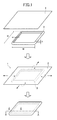
- FIGS. 1 and 2 The reflecting mirror of the present invention will be described below using FIGS. 1 and 2 , to which the inventive reflecting mirror is not particularly limited.
- FIG. 1 is an oblique view schematically illustrating an example of a preferred embodiment of the reflecting mirror for solar radiation collection of the present invention from the perspective of its production process.
- FIG. 2 is a schematic end view showing the cross section along section line A-A in FIG. 1 .
- a reflecting mirror 1 has a film mirror 2 and a frame-shaped support member 3 which supports a peripheral edge of the film mirror 2.
- the support member 3 is in contact with the film mirror 2, and has a curved face 3b convexed outward in a horizontal direction with respect to an opening face 3a of the support member 3.
- a letter C denotes the amount of warpage ( ⁇ m) of the film mirror as described above
- a number 5 denotes the point in a cross section perpendicular to the opening face 3a of the support member 3 at which the film mirror 2 and the support member 3 separate from each other (hereafter also referred to as "exit point").
- the film mirror to be included in the reflecting mirror of the present invention is not particularly limited in shape or layer configuration provided that its film thickness is 0.10 to 0.30 mm, and any conventional film mirror may be used.
- the film thickness of the film mirror is preferably 0.12 to 0.27 mm and more preferably 0.15 to 0.25 mm because tension adjustment of the film mirror is easy when the support member to be described later supports the peripheral edge and also because the specular reflectivity further improves and the weather resistance is better.
- the shape of the film mirror is not particularly limited but may be circular or polygonal. Since it is easier to provide and adjust film mirror tension when the support member to be described later supports the peripheral edge, a polygonal shape is preferred and a rectangular shape is more preferred.
- the size of the film mirror is not particularly limited because it can be designed as appropriate according to the shape thereof, the type of a mounting body, and the like.
- the size of a rectangular film mirror (longitudinal width and lateral width) it is preferable from the viewpoint of tension adjustment that the longitudinal width (long side) is 100 to 5000 mm, the lateral width (short side) is 100 to 2000 mm, and the ratio between the longitudinal width and the lateral width (longitudinal width/lateral width) is 1/1 to 15/1.
- FIGS. 3 to 6 are section views schematically illustrating examples of preferred embodiments of the film mirror included in the reflecting mirror of the present invention.
- the layer structure of the film mirror is not particularly limited to these drawings, and if necessary, a primer layer or an adhesive layer may be provided between adjacent layers, or a back coat layer may be provided at the side facing the mounting body, for example.
- Examples of a first embodiment of the film mirror include an embodiment as illustrated in FIG. 3 in which a film mirror 10 has a resin substrate 11, a metallic reflective layer 12, and a surface covering layer 13 in this order from the side to face the mounting body (not illustrated), and an embodiment as illustrated in FIG. 4 in which a film mirror 10 has the metallic reflective layer 12, the resin substrate 11, and the surface covering layer 13 in this order from the side to face the mounting body (not illustrated).
- a covering layer which protects the metallic reflective layer may be provided on the surface of the metallic reflective layer 12 that is opposite from the side to face the resin substrate 11.
- Examples of a second embodiment of the film mirror include an embodiment as illustrated in FIG. 5 in which a film mirror 100 has a first surface covering layer 101, a first metallic reflective layer 102, a resin substrate 103, a second metallic reflective layer 104, and a second surface covering layer 105 in this order from the side to face the mounting body (not illustrated), and an embodiment as illustrated in FIG. 6 in which a film mirror 100 has the first surface covering layer 101, a first resin substrate 106, a metallic reflective layer 107, a second resin substrate 108, and the second surface covering layer 105 in this order from the side to face the mounting body (not illustrated).
- a reflecting mirror including the film mirror 2 as shown in FIG. 1 for instance, that has an additional support member provided on its surface opposite to the support member 3 is preferred from the perspective that both faces of the film mirror can be used by reversing the reflecting mirror relative to the mounting body.
- the resin substrate (including the first resin substrate and the second resin substrate; the same applying in the rest) is not particularly limited, and examples of the constituent material thereof include polyolefin resins such as polyethylene and polypropylene; polyester resins such as polyethylene terephthalate and polyethylene naphthalate; polycarbonate resins; acrylic resins such as polymethyl methacrylate; polyamide resins, polyimide resins; polyvinyl chloride resins; polyphenylene sulfide resins; polyether sulfone resins; polyethylene sulfide resins; polyphenylene ether resins; styrene resins; cellulose resins such as cellulose acetate; and so forth.
- the constituent materials of the first resin substrate and the second resin substrate used in the second embodiment may be the same or different materials.
- polyester resins or acrylic resins are preferred from the perspectives of reflectance and weather resistance of the resultant film mirror.
- the shape of the resin substrate is not limited to a planar shape, and may be, for example, any of concave, convex and other shapes.
- the thickness of the resin substrate is not particularly limited because it varies depending on the shape thereof, but when the resin substrate is planar, a thickness of from 25 to 300 ⁇ m is usually preferred.
- the metallic reflective layer (including the first metallic reflective layer and the second metallic reflective layer; the same applying in the rest) is not particularly limited, and examples of the constituent material (metal) thereof include Au, Ag, Cu, Pt, Pd, In, Ga, Sn, Ge, Sb, Pb, Zn, Bi, Fe, Ni, Co, Mn, Tl, Cr, V, Ru, Rh, Ir, Al, and the like.
- the constituent materials of the first metallic reflective layer and the second metallic reflective layer used in the second embodiment ( FIG. 5 ) may be the same or different materials.
- Ag is preferred and Ag is more preferred from the perspectives of reflectance and weather resistance of the resultant film mirror.
- the content of Ag in the metallic reflective layer is preferably not less than 30 mol%, more preferably not less than 50 mol%, even more preferably not less than 80 mol%, particularly preferably not less than 95 mol%, and most preferably 100 mol% relative to all metals constituting the metallic reflective layer.
- the metallic reflective layer is not particularly limited for shape and may be a layer that covers all or part of the main face of the resin substrate.
- the thickness of the metallic reflective layer is not particularly limited, but from the perspectives of reflectance and the like of the film mirror, it is preferably from 50 to 500 nm, and more preferably from 70 to 300 nm.
- a method of forming the metallic reflective layer is not particularly limited, and either a wet method or a dry method may be employed.
- wet methods include known methods such as so-called metal plating methods (electroless plating or electroplating), and a method of applying a solution containing a metal complex compound.
- dry methods include vacuum evaporation, sputtering, ion plating, and the like.
- An example of a preferred embodiment of a metallic reflective layer formation method in the present invention is a method in which (i) a primer layer is formed on the resin substrate, (ii) a plating catalyst or a precursor thereof is applied to the formed primer layer, (iii) plating is performed on the primer layer to which the plating catalyst or the precursor thereof has been applied.
- Step (i) is a step in which a primer layer is formed on a resin substrate.
- the primer layer is a layer disposed between the resin substrate and the metallic reflective layer and serving to increase the adhesion therebetween.
- the primer layer is obtained by performing at least one of heat treatment and photoirradiation treatment (also referred to as "energy application” hereinafter) on a layer containing a polymer having a functional group that interacts with a plating catalyst or a precursor thereof and a polymerizable group.
- heat treatment and photoirradiation treatment also referred to as "energy application” hereinafter
- the polymer used in the primer layer contains a functional group that interacts with a plating catalyst or a precursor thereof (also referred to as "interactive group” hereinafter) and a polymerizable group.
- the interactive group is a group that interacts with a plating catalyst or a precursor thereof, and has the role of increasing adhesion between the metallic reflective layer and the primer layer.
- the polymerizable group undergoes cross-linking reaction to thereby increase the strength of the primer layer while a part of the polymerizable group reacts with the resin substrate to thereby increase adhesion between the resin substrate and the primer layer.
- the polymerizable group is not limited as long as it is a functional group that can form, upon energy application, chemical bonds among polymers or between a polymer and the resin substrate.
- Examples of the polymerizable group include radical-polymerizable groups, cationic-polymerizable groups, and the like. Of these, radical-polymerizable groups are preferred from the perspective of reactivity.
- radical-polymerizable groups examples include a methacryloyl group, an acryloyl group, an itaconate group, a crotonate group, an isocrotonate group, a maleate group, a styryl group, a vinyl group, an acrylamide group, a methacrylamide group, and the like.
- a methacryloyl group, an acryloyl group, a vinyl group, a styryl group, an acrylamide group, and a methacrylamide group are preferred.
- a methacryloyl group, an acryloyl group, an acrylamide group, and a methacrylamide group are more preferred from the perspectives of radical polymerization reactivity and flexibility in synthesis, and an acrylamide group and a methacrylamide group are even more preferred from the perspective of alkali resistance.
- the type of interactive group is not particularly limited provided that it is a group that interacts with a plating catalyst or a precursor thereof, and examples thereof include nitrogen-containing functional groups such as an amino group, an amide group, an imide group, a urea group, a tertiary amino group, an ammonium group, an amidine group, a triazine ring, a triazole ring, a benzotriazole group, an imidazole group, a benzimidazole group, a quinoline group, a pyridine group, a pyrimidine group, a pyrazine group, a quinazoline group, a quinoxaline group, a purine group, a triazine group, a piperidine group, a piperazine group, a pyrrolidine group, a pyrazole group, an aniline group, groups containing an alkylamine structure, groups containing an isocyanuric structure, a nitro group, a nitro
- ionic polar groups such as a carboxyl group, a sulfonate group, a phosphate group, and a boronic acid group
- nondissociative functional groups such as an ether group or a cyano group
- the polymer preferably contains a unit (repeating unit) represented by formula (1) below and a unit represented by formula (2) below.
- R 10 denotes a hydrogen atom or an alkyl group (for example, a methyl group, an ethyl group, or the like).
- L 2 denotes a single bond or a divalent linking group.
- the divalent linking group include optionally substituted divalent aliphatic hydrocarbon groups (preferably having from 1 to 8 carbons; for example, alkylene groups such as a methylene group, an ethylene group, or a propylene group), optionally substituted divalent aromatic hydrocarbon groups (preferably having from 6 to 12 carbons; for example, a phenylene group), and -O-, -S-, -SO 2 -, -N(R)- (wherein R is an alkyl group), -CO-, -NH-, -COO-, - CONH-, or a group in which these are combined (for example, an alkyleneoxy group, an alkyleneoxycarbonyl group, an alkylenecarbonyloxy group, and the like), and the like.
- R 11 denotes an interactive group.
- the definition, specific examples, and preferred embodiments of the interactive group are as described above.
- the polymer may contain two or more kinds of units represented by formula (1) having different interactive groups denoted by R 11 .
- R 11 a unit represented by formula (1) in which R 11 is an ionic polar group and a unit represented by formula (1) in which R 11 is a nondissociative group may be contained in the polymer.
- R 12 to R 15 denote, each independently, a hydrogen atom or an optionally substituted alkyl group.
- R 12 to R 15 are optionally substituted alkyl groups
- alkyl groups having from 1 to 6 carbons are preferred, and alkyl groups having from 1 to 4 carbons are more preferred.
- examples of unsubstituted alkyl groups include a methyl group, an ethyl group, a propyl group, and a butyl group.
- substituted alkyl groups include a methyl group, an ethyl group, a propyl group, and a butyl group substituted with a methoxy group, a hydroxy group, a halogen atom (for example, a chlorine atom, a bromine atom, or a fluorine atom) or the like.
- R 12 a hydrogen atom, a methyl group, or a methyl group substituted with a hydroxy group or a bromine atom is preferred.
- R 13 a hydrogen atom, a methyl group, or a methyl group substituted with a hydroxy group or a bromine atom is preferred.
- R 14 a hydrogen atom is preferred.
- R 15 a hydrogen atom is preferred.
- L 3 denotes a single bond or a divalent linking group. Specific examples and preferred embodiments of the divalent linking group are the same as those of L 2 in formula (1).
- the most preferred ranges of the polymer include a copolymer containing a unit represented by formula (A) below, a unit represented by formula (B) below and a unit represented by formula (C) below, a copolymer containing a unit represented by formula (A) below and a unit represented by formula (B) below, and a copolymer containing a unit represented by formula (A) below and a unit represented by formula (C) below.
- R 21 to R 26 denote, each independently, a hydrogen atom or an optionally substituted alkyl group having from 1 to 4 carbons.
- X, Y, Z, and U denote, each independently, a single bond or a divalent linking group.
- L 4 , L 5 , and L 6 denote, each independently, a single bond or a divalent linking group.
- W denotes an interactive group consisting of a nondissociative functional group.
- V denotes an interactive group consisting of an ionic polar group. Specific examples and preferred embodiments of the divalent linking group are the same as those of L 2 in formula (1).
- Y and Z are preferably, each independently, an ester group, an amide group, or a phenylene group (-C 6 H 4 -).
- L 4 is preferably an optionally substituted divalent organic group (especially a hydrocarbon group) having from 1 to 10 carbons.
- W is preferably a cyano group or an ether group.
- X and L 5 are both preferably single bonds.
- V is preferably a carboxylic acid group
- V is a carboxylic acid group and L 6 contains a ring structure having from 4 to 8 members at a portion linked to V
- V is a carboxylic acid group and the chain length of L 6 is from 6 to 18 atoms
- an embodiment in which V is a carboxylic acid group and U and L 6 are single bonds is also preferred.
- an embodiment in which V is a carboxylic acid group and U and L 6 are both single bonds is most preferred.
- the ratio of unit represented by formula (A) : unit represented by formula (B) : unit represented by formula (C) is preferably from 5 to 50 mol% : from 5 to 40 mol% : from 20 to 70 mol%, and more preferably from 10 to 40 mol% : from 10 to 35 mol% : from 20 to 60 mol%.
- the ratio of unit represented by formula (A) : unit represented by formula (B) is preferably from 5 to 50 mol% : from 50 to 95 mol%, and more preferably from 10 to 40 mol% : from 60 to 90 mol%.
- the ratio of unit represented by formula (A) : unit represented by formula (C) is preferably from 5 to 50 mol% : from 50 to 95 mol%, and more preferably from 10 to 40 mol% : from 60 to 90 mol%.
- the improvement in polymerization of the polymer by heat treatment or photoirradiation treatment, the decrease in resistance of the primer layer, the improvement in moisture-resistant adhesion, and the like are achieved.
- the method of forming a layer containing the above polymer is not particularly limited, and a known method may be employed.
- One example is a method in which a composition for forming the layer containing the above polymer is applied to the resin substrate, and then dried as necessary to form the layer.
- At least one of heat treatment and photoirradiation treatment is performed on the layer containing the polymer.
- the layer containing the polymer may be subjected to one or both of heat treatment and photoirradiation treatment. When both treatments are performed, they may be performed in separate steps or simultaneously.
- the polymerizable groups are activated, reactions of the polymerizable groups with each other and between the polymerizable group and the resin substrate proceed, and the primer layer adhered on the resin substrate is formed.
- the optimal heat treatment conditions are selected according to the type of polymer used, but it is preferable that treatment be performed at a temperature of from 60 to 150°C (more preferably from 80 to 120°C) for from 0.1 to 3 hours (more preferably from 0.5 to 2 hours) from the perspectives that crosslink density of the primer layer is increased and weather resistance and flexibility of the film mirror are improved.
- the optimal photoirradiation treatment conditions are selected according to the type of polymer used, but it is preferable that the exposure quantity be from 10 to 8000 mJ/cm 2 , and preferably from 100 to 3000 mJ/cm 2 , from the perspectives that crosslink density of the primer layer is increased and weather resistance and flexibility of the film mirror are improved.
- the exposure wavelength is preferably from 200 to 300 nm.
- the light source used in exposure is not particularly limited, and may be, for example, a mercury lamp, a metal halide lamp, a xenon lamp, a chemical lamp, a carbon arc lamp, or the like.
- Exemplary radioactive rays include an electron beam, an X-ray, an ion beam, a far-infrared ray, and the like.
- An unreacted polymer may be removed from the composition after heat treatment or photoirradiation treatment as appropriate.
- the removal method include methods using solvents.
- solvents include a solvent that dissolves a polymer, and, in the case of an alkali-soluble polymer, alkali-based developing solutions (sodium carbonate, sodium hydrogen carbonate, ammonia water, sodium hydroxide aqueous solution) and the like may be used for removal.
- the thickness of the primer layer is not particularly limited but is preferably from 0.05 to 10 ⁇ m, and more preferably from 0.3 to 5 ⁇ m, because weather resistance and flexibility of the film mirror are excellent.
- the catalyst provision step is a step in which a plating catalyst or a precursor thereof is provided to the primer layer.
- the interactive group in the primer layer adsorbs the plating catalyst or the precursor thereof.
- the primer layer adsorbs the metal ion.
- Examples of the plating catalyst or the precursor thereof are those that function as catalysts or electrodes in plating in “Step (iii): Plating step" to be described below. Therefore, the plating catalyst or the precursor thereof is determined depending on the type of plating in the plating step.
- the plating catalyst for example, an electroless plating catalyst
- the precursor thereof used will be described in detail below.
- an electroless plating catalyst one that can become an active nucleus during electroless plating is preferred and examples thereof include metals having catalytic ability in an auto-catalytic reduction reaction (metals known as being capable of electroless plating and having an ionization tendency lower than that of Ni), specifically Pd, Ag, Cu, Ni, Al, Fe, Co, and the like. Among these, Pd or Ag is preferred due to high catalytic ability.
- an electroless plating catalyst precursor one that can become an electroless plating catalyst by chemical reaction is preferred.
- a metal ion of a metal cited above as an electroless plating catalyst may be used.
- the metal ion that is the electroless plating catalyst precursor becomes by a reduction reaction a zero-valent metal which is an electroless plating catalyst.
- An electroless plating catalyst may be formed by providing the metal ion that is an electroless plating catalyst precursor to the primer layer and then independently changing the metal ion to a zero-valent metal by a reduction reaction prior to the immersion into the electroless plating bath, or the metal ion may be immersed as the electroless plating catalyst precursor into an electroless plating bath to allow the metal ion to be changed to a metal (electroless plating catalyst) using a reducing agent in the electroless plating bath.
- the metal ion that is the electroless plating catalyst precursor is preferably provided to the primer layer using a metal salt.
- the metal salt used is not particularly limited provided that it is dissociated into a metal ion and a base (anion) when dissolved in an appropriate solvent, and examples thereof include M(NO 3 ) n , MCl n , M 2/n (SO 4 ), M 3/n (PO 4 )Pd(OAc) n (where M denotes a metal atom of valence n), and the like.
- M(NO 3 ) n MCl n , M 2/n (SO 4 ), M 3/n (PO 4 )Pd(OAc) n (where M denotes a metal atom of valence n)
- M denotes a metal atom of valence n
- the metal ion examples include Ag ion, Cu ion, Al ion, Ni ion, Co ion, Fe ion, and Pd ion.
- the metal ion examples include Ag ion, Cu ion, Al ion, Ni ion, Co ion, Fe ion, and Pd ion.
- Ag ion, Cu ion, and Pd ion are particularly preferred due to the number of types of coordinatable functional groups and catalytic ability.
- the reduction step may be performed as a separate step prior to electroless plating by preparing a catalyst activating solution (reducing solution).
- the catalyst activating solution often contains a reducing agent that can reduce the electroless plating catalyst precursor (primarily a metal ion) to a zero-valent metal, and a pH adjusting agent for activating the reducing agent.
- the concentration of the reducing agent relative to the total solution is preferably from 0.1 to 10 wt%.
- Boron-based reducing agents such as sodium borohydride and dimethylamine borane and reducing agents such as formaldehyde and hypophosphorous acid may be used as the reducing agent.
- reduction is performed preferably with an alkaline aqueous solution containing formaldehyde.
- a catalyst used for performing electroplating without performing electroless plating may be used as the plating catalyst.
- catalysts include zero-valent metals, and more specifically, Pd, Ag, Cu, Ni, Al, Fe, Co, and the like. Among these, those capable of multidentate coordination are preferred, and Pd, Ag, and Cu are particularly preferred due to their high adsorption (attachment) properties with respect to interactive groups and high catalytic ability.
- a solution containing the plating catalyst or the precursor thereof for example, a dispersion in which a metal is dispersed in an appropriate dispersion medium, or a solution containing a dissociated metal ion prepared by dissolving a metal salt in an appropriate solvent
- the dispersion or the solution is applied to the primer layer, or the resin substrate on which the primer layer has been formed is immersed in the dispersion or the solution.
- the plating step is a step in which the metallic reflective layer is formed by plating on the primer layer to which the metal catalyst or the precursor thereof has been provided.
- the type of plating performed in this step may be electroless plating or electroplating, and can be selected as appropriate depending on the function of the plating catalyst or the precursor thereof provided to the primer layer in the catalyst provision step above.
- either of electroplating or electroless plating may be performed on the primer layer to which the plating catalyst or precursor thereof has been provided.
- Electroless plating refers to an operation of depositing a metal by a chemical reaction using a solution in which a metal ion of metal to be deposited for plating is dissolved.
- Electroless plating is performed by, for example, cleaning a resin substrate having a primer layer to which an electroless plating catalyst has been provided using water to remove an excess electroplating catalyst (metal), and then immersing the resin substrate in an electroless plating bath.
- a known electroless plating bath may be used as the electroless plating bath.
- a resin substrate having a primer layer to which an electroless plating catalyst precursor has been provided is immersed in an electroless plating bath in the state where the primer layer is adsorbed or impregnated with the electroless plating catalyst precursor, it is preferred that the substrate be cleaned to remove an excess precursor (metal salt or the like) and then immersed in the electroless plating bath. In this case, reduction of the plating catalyst precursor and subsequent electroless plating are performed in the electroless plating bath.
- a known electroless plating bath may be used as the electroless plating bath.
- electroplating can be performed on the primer layer to which the plating catalyst or the precursor thereof has been provided.
- a conventional method known in the art may be used as the electroplating method in the present invention.
- the metal used in electroplating in this step include copper, chromium, lead, nickel, gold, silver, tin, zinc, and the like, and silver is preferred because it further improves the reflectance of the resultant film mirror.
- electroplating may be further performed using the formed plating film as an electrode.
- silver compounds used in plating include silver nitrate, silver acetate, silver sulfate, silver carbonate, silver methanesulfonate, ammoniacal silver, silver cyanide, silver thiocyanate, silver chloride, silver bromide, silver chromate, silver chloranilate, silver salicylate, silver diethyldithiocarbamate, diethyldithiocarbamic acid silver salt, and silver p-toluenesulfonate.
- silver methanesulfonate is preferred because it further improves the reflectance of the resultant film mirror.
- the surface covering layer (including the first surface covering layer and the second surface covering layer; hereinafter the same) is not particularly limited, and the constituent material thereof is not limited as long as it has transparency capable of transmitting light.
- the constituent material include resin, glass, ceramic, and the like, among which resin is preferred due to its excellent flexibility.
- the resin examples include photocurable resins such as urethane (meth)acrylate resin, polyester (meth)acrylate resin, silicone (meth)acrylate resin, and epoxy (meth)acrylate resin; heat-curable resins such as phenol resin, urea resin, phenoxy resin, silicone resin, polyimide resin, diallyl phthalate resin, furan resin, bismaleimide resin, and cyanate resin; thermoplastic resins such as phenoxy resin, polyether sulfone, polysulfone, and polyphenylene sulfone; and the like.
- the constituent materials of the first surface covering layer and the second surface covering layer used in the second embodiment may be the same or different materials.
- the thickness of the surface covering layer is not particularly limited but is preferably from 10 to 200 ⁇ m, and more preferably from 25 to 100 ⁇ m, because weather resistance and flexibility of the film mirror are more excellent.
- the method of forming the surface covering layer is not particularly limited, and examples thereof include a method in which a predetermined resin substrate is adhered to the metallic reflective layer, and a method in which a curable composition containing the photocurable resin or the heat-curable resin described above is applied to the metallic reflective layer and then photocured by ultraviolet irradiation or heat-cured by heat.
- the constituent material of the optional primer layer is not particularly limited provided that it can improve adhesion between layers, and specific examples thereof include resin materials such as polyester resin, urethane resin, acrylic resin, urethane acrylic resin, polyamide resin, cycloolefin polymer resin, and the like.
- the thickness of the primer layer is not particularly limited, but is preferably from 0.1 to 50 ⁇ m, and more preferably from 1 to 30 ⁇ m.
- the method of forming the primer layer is not particularly limited.
- urethane acrylic resin for example, Ebecryl 8402, manufactured by Daicel-Cytec Co., Ltd.
- a photopolymerization initiator for example, Irgacure 184, manufactured by Ciba Specialty Chemicals
- the constituent material of the optional adhesive layer is not particularly limited provided that it has satisfactory adhesion and smoothness, and specific examples thereof include polyester resin, acrylate resin, melamine resin, epoxy resin, polyamide resin, vinyl chloride resin, vinyl chloride-vinyl acetate copolymer resin, and the like. One of these may be used alone, or two or more may be used together.
- the thickness of the adhesive layer is not particularly limited, but is preferably from 0.01 to 5 ⁇ m, and more preferably from 0.1 to 2 ⁇ m, from the perspectives of adhesion, smoothness, reflectance, and the like.
- the method of forming the adhesive layer is not particularly limited.
- a conventional known coating method such as gravure coating, reverse coating, die coating, a blade coater, a roll coater, an air knife coater, a screen coater, a bar coater, a curtain coater, or the like may be used.
- the material for forming the optional back coat layer is not particularly limited, and examples thereof include urethane resin, the resins contained in the surface covering layer described above, and the like.
- the thickness of the back coat layer is not particularly limited, but is preferably from 0.5 to 50 ⁇ m, and more preferably from 1 to 30 ⁇ m.
- the method of forming the back coat layer is not particularly limited.
- a curable composition containing any of these resins is applied to the back face of the resin substrate and then photocured by ultraviolet irradiation or heat-cured by heat.
- the support member in the reflecting mirror of the present invention is a frame-shaped support member supporting a peripheral edge of the film mirror as described above, and the frame-shaped support member as such is in contact with the film mirror and has a curved face convexed outward in a horizontal direction with respect to an opening face of the support member, with the radius of curvature of the curved face being not less than 8 mm.
- the support member is not particularly limited in shape of a cross section parallel to the opening face, and the shape of such a cross section may be circular or polygonal, as is the case with the shape of the film mirror. Since it is easier to provide and adjust film mirror tension, a polygonal shape is preferred and a rectangular (quadrangular) shape is more preferred.
- the support member has the cross section perpendicular to the opening face whose shape (hereafter also referred to as "perpendicular cross-sectional shape”) represents that the support member has, in a portion thereof in contact with the film mirror, a curved face convexed outward in a horizontal direction with respect to the opening face of the support member and having a radius of curvature of not less than 8 mm.
- the support member 3 has the curved face 3b which is convexed outward in a horizontal direction with respect to the opening face 3a of the support member 3 in a portion in contact with the film mirror 2, and the radius of curvature of the curved face 3b is not less than 8 mm.
- the support member which has a curved face of the radius of curvature as specified above, tension can be applied to the film mirror with a prescribed thickness as described above while keeping the amount of warpage small, and as a result, the reflecting mirror of the present invention is excellent in specular reflectivity and light-collecting characteristics.
- the ratio between the radius of curvature (not less than 8 mm) of the curved face of the support member and the film thickness (0.10 to 0.30 mm) of the film mirror is preferably not less than 80, more preferably not less than 90, and even more preferably 90 to 260.
- the radius of curvature of the curved face of the support member is preferably not less than 15 mm and more preferably 15 to 30 mm.
- the angle (hereafter referred to as "exit angle”) formed by a tangent to the support member and the opening face of the support member at the point in a cross section perpendicular to the opening face of the support member where the film mirror and the support member separate from each other (namely, the point represented as the exit point 5 in FIG. 2 and in FIG. 7 to be described later) is preferably 0° or greater but up to 20°, and more preferably 5 to 15°.
- FIGS. 7(A) to 7(F) The perpendicular cross-sectional shape of the support member will be described in detail below using FIGS. 7(A) to 7(F) .
- FIGS. 7(A) to 7(F) are examples of a schematic section view taken along section line B-B in FIG. 1 , to which examples the perpendicular cross-sectional shape of the support member is not limited.
- the perpendicular cross-sectional shape of the support member is not particularly limited provided that it represents the curved face as described above, and may be a shape consisting of a round part and a rectangular part (in an oblong shape) as illustrated in FIG. 7(A) , or a circular shape containing a curved face as illustrated in FIGS. 7(B) and 7(C) , or a shape consisting of a round part and a rectangular part (in a trapezoidal shape) as illustrated in FIGS. 7(D) to 7(F) .
- FIGS. 7(A) to 7(C) each show an example in which the exit angle is 0°, while FIG. 7(D) shows an example in which the exit angle ⁇ is 10°.
- FIG. 7(E) shows an example in which the exit angle ⁇ is 15°, and
- FIG. 7(F) shows an example in which the exit angle ⁇ is 30°.
- the material that constitutes the support member is not particularly limited, and specific examples thereof include metal materials such as stainless steel (SUS), aluminum, aluminum alloy, and titanium; resin materials such as carbon fiber-reinforced plastic, polyether ether ketone (PEEK), and polyphenylene sulfide (PPS); and the like.
- metal materials such as stainless steel (SUS), aluminum, aluminum alloy, and titanium
- resin materials such as carbon fiber-reinforced plastic, polyether ether ketone (PEEK), and polyphenylene sulfide (PPS); and the like.
- the metal materials are preferred from the perspective of bonding to the mounting body since the mounting body is often composed of a metal material, and stainless steel or aluminum is more preferred.
- the thickness of the support member is not particularly limited, but from 1 to 10 mm is preferred, and from 2 to 5 mm is more preferred.
- the width of a constituent member (frame member) of the support member (w in FIG. 1 ) is not particularly limited, but from 10 to 50 mm is preferred, and from 15 to 30 mm is more preferred.
- the longitudinal width (long side) of the entire support member (H in FIG. 1 ) is preferably from 100 to 5000 mm
- the lateral width (short side) (W in FIG. 1 ) is preferably from 100 to 2000 mm
- the ratio of the longitudinal width to the lateral width (longitudinal width/lateral width) is preferably from 1/1 to 10/1.
- the method for producing the reflecting mirror of the present invention is not particularly limited but may include overlaying the film mirror 2 having a larger size than the support member 3 on the support member 3 and folding end portions of the film mirror 2 in directions of dashed arrows while applying tension to the film mirror 2 in directions of solid arrows, so as to bond them to the support member 3, as illustrated in FIG. 1 .
- the reflecting mirror may be produced by temporarily fixing the film mirror under a certain degree of tension to a frame for temporary fixing (temporary frame) having a larger size (H ⁇ W) and a smaller thickness (t) than the support member using adhesive tape or the like and pasting the support member with a pressure-sensitive adhesive applied thereto perpendicularly on the temporarily fixed film mirror, then pressing the support member inside the temporary frame to thereby bond (adhere) the peripheral edge of the film mirror to the support member.
- temporary frame temporary fixing
- H ⁇ W size
- t thickness
- the method for bonding an end portion of the film mirror to the support member is not particularly limited, and may be, for example, an adhesion method using an adhesive or a pressure-sensitive adhesive, a method for fixing the two to each other using clips, and the like.
- a region where the peripheral edge of the film mirror and the support member are bonded together has at least two through-holes which are used in bonding to the mounting body, such as a solar reflector body (solar radiation tracking system).
- the support member and the mounting body can be easily anchored to each other using screws, bolts or the like.
- a solution containing the acrylic polymer represented by formula (3) was applied by spin-coating to a thickness of 500 nm, and this was dried at 80°C for 5 minutes to produce a coating film.
- numeric values in formula (3) represent the proportions (mol%) of the respective units.
- the method of synthesizing the acrylic polymer represented by formula (3) is as follows.
- N,N-Dimethylacetamide in an amount of 8 g was introduced into a 500 mL three-necked flask and heated to 65°C under nitrogen flow.
- 14.3 g of the monomer M1 obtained above 3.0 g of acrylonitrile (manufactured by Tokyo Chemical Industry Co., Ltd.), 6.5 g of acrylic acid (manufactured by Tokyo Chemical Industry Co., Ltd.), and a solution in which 0.4 g of V-65 (manufactured by Wako Pure Chemical Industries, Ltd.) was dissolved in 8 g of N,N-dimethylacetamide was added dropwise over the course of 4 hours. After dropwise addition was completed, the mixture was stirred for another 3 hours.
- the method of preparing a solution containing the acrylic polymer represented by formula (3) is as follows.
- the acrylic polymer represented by formula (3) (7 parts by weight), 1-methoxy-2-propanol (74 parts by weight), and water (19 parts by weight) were mixed, and a photopolymerization initiator (Esacure KTO-46, manufactured by Lamberti) (0.35 parts by weight) was added to this mixed solution.
- a photopolymerization initiator (Esacure KTO-46, manufactured by Lamberti) (0.35 parts by weight) was added to this mixed solution.
- the mixture was mixed with stirring and a solution containing the acrylic polymer represented by formula (3) was obtained.
- the coating film above was irradiated with light at a wavelength of 254 nm using a UV exposure device manufactured by San-ei Electric Co., Ltd. (model: UVF-502S, lamp: UXM-501MD) with a cumulative exposure of 1000 mJ/cm 2 , thereby forming a primer layer (thickness: 500 nm).
- the PET substrate with the primer layer was immersed in 1 wt% aqueous solution of sodium hydrogen carbonate for 5 minutes, and then washed with pure water.
- the PET substrate with the primer layer was immersed in 1 wt% aqueous solution of silver nitrate aqueous solution for 5 minutes and then washed with pure water to thereby obtain a PET substrate with a primer layer to which an electroless plating catalyst precursor (silver ions) had been provided.
- an electroless plating catalyst precursor silver ions
- the obtained resin substrate with the primer layer was immersed in an alkali aqueous solution (pH 12.5) containing 0.14 wt% NaOH and 0.25 wt% formalin (serving as a reducing agent) for 1 minute and then washed with pure water to thereby obtain a PET substrate with a primer layer to which a reducing metal (silver) had been provided.
- an alkali aqueous solution pH 12.5 containing 0.14 wt% NaOH and 0.25 wt% formalin (serving as a reducing agent) for 1 minute and then washed with pure water to thereby obtain a PET substrate with a primer layer to which a reducing metal (silver) had been provided.
- the following electroplating process was performed on the primer layer to which the reducing metal (silver) had been provided, and a metallic (silver) reflective layer with a thickness of 200 nm was formed on the primer layer.
- DAIN Silver Bright PL-50 (manufactured by Daiwa Fine Chemicals Co., Ltd.) adjusted to a pH of 9.0 using 8M potassium hydroxide was used as the electroplating solution.
- the PET substrate with the primer layer having a reducing metal on the surface was immersed in the electroplating solution and plated for 15 seconds at 0.5 A/dm 2 , and then washed in flowing pure water for 1 minute.
- an urethane adhesive product name: LIS825, LCR901, manufactured by Toyo Ink Co., Ltd
- LIS825, LCR901, manufactured by Toyo Ink Co., Ltd was applied to the metallic reflective layer and dried for 5 minutes to produce an adhesive layer (thickness: 8 ⁇ m).
- a PMMA substrate HBS006, thickness: 50 ⁇ m, manufactured by Mitsubishi Rayon Co., Ltd.
- Table 1 below shows the size and the film thickness of the film mirror produced, the type of resin substrate, the type of reflective layer, and the type of surface covering layer.
- ⁇ 700 mm in the Size column means 700 mm ⁇ 700 mm square.
- the produced film mirror was temporarily fixed to a frame for temporary fixing (size, 700 mm ⁇ 700 mm square; width, 25 mm; thickness, 5 mm) using adhesive tape while a certain degree of tension was applied.
- a pressure-sensitive adhesive (FINETAC manufactured by DIC Corp.) was applied to the frame surface of a frame-shaped support member made of aluminum (A5052) (size, 500 mm ⁇ 500 mm square; width, 25 mm; thickness, 10 mm; the perpendicular cross-sectional shape as shown in FIG. 7 (A) ; exit angle, 0°; radius of curvature, 9 mm).
- the surface of the support member to which the pressure-sensitive adhesive had been applied was pasted perpendicularly on the film mirror temporarily fixed to the frame for temporary fixing (temporary frame), and the support member was further pressed inside the temporary frame to thereby produce a reflecting mirror.
- Table 1 below shows the size, the perpendicular cross-sectional shape, the exit angle, and the radius of curvature of the support member used, and also shows the ratio between the radius of curvature of the support member and the film thickness of the film mirror (radius of curvature/film thickness), and the method of bonding a film mirror and a support member.
- ⁇ 500 mm in the Size column means 500 mm ⁇ 500 mm square.
- a reflecting mirror was produced by the same method as in Example 1 except that the thickness of the PET substrate was changed to 150 ⁇ m and the film thickness of the film mirror was 0.21 mm.
- a reflecting mirror was produced by the same method as in Example 1 except that the thickness of the PET substrate was changed to 220 ⁇ m and the film thickness of the film mirror was 0.28 mm.
- a reflecting mirror was produced by the same method as in Example 2 except that a primary layer was not formed and a metallic reflective layer formed by the method described below was used.
- a metallic reflective layer having eight TiO 2 layers and seven SiO 2 layers was formed by alternately forming layers of TiO 2 with a thickness of 65 nm and layers of SiO 2 with a thickness of 110 nm by sputtering (PVD) on a PET substrate (thickness, 150 ⁇ m; manufactured by Fujifilm Corporation).
- PVD sputtering
- a reflecting mirror was produced by the same method as in Example 2 except that instead of the frame-shaped support member made of aluminum (A5052) (size, 500 mm ⁇ 500 mm square; width, 25 mm; thickness, 10 mm; the perpendicular cross-sectional shape as shown in FIG. 7(A) ; exit angle, 0°; radius of curvature, 9 mm), a frame-shaped support member made of stainless steel (SUS304) (size, 500 mm ⁇ 500 mm square; width, 25 mm; thickness, 10 mm; the perpendicular cross-sectional shape as shown in FIG. 7(A) ; exit angle, 0°; radius of curvature, 9 mm) was used.
- SUS304 stainless steel
- a reflecting mirror was produced by the same method as in Example 1 except that instead of the frame-shaped support member made of aluminum (A5052) (size, 500 mm ⁇ 500 mm square; width, 25 mm; thickness, 10 mm; the perpendicular cross-sectional shape as shown in FIG. 7(A) ; exit angle, 0°; radius of curvature, 9 mm), a frame-shaped support member made of aluminum (A5052) (size, 500 mm ⁇ 500 mm square; width, 25 mm; thickness, 10 mm; the perpendicular cross-sectional shape as shown in FIG. 7(B) ; exit angle, 0°; radius of curvature, 18 mm) was used.
- a reflecting mirror was produced by the same method as in Example 6 except that the thickness of the PET substrate was changed to 150 ⁇ m and the film thickness of the film mirror was 0.21 mm.
- a reflecting mirror was produced by the same method as in Example 6 except that the thickness of the PET substrate was changed to 220 ⁇ m and the film thickness of the film mirror was 0.28 mm.
- a reflecting mirror was produced by the same method as in Example 1 except that instead of the frame-shaped support member made of aluminum (A5052) (size, 500 mm ⁇ 500 mm square; width, 25 mm; thickness, 10 mm; the perpendicular cross-sectional shape as shown in FIG. 7(A) ; exit angle, 0°; radius of curvature, 9 mm), a frame-shaped support member made of aluminum (A5052) (size, 500 mm ⁇ 500 mm square; width, 25 mm; thickness, 10 mm; the perpendicular cross-sectional shape as shown in FIG. 7(C) ; exit angle, 0°; radius of curvature, 28 mm) was used.
- a reflecting mirror was produced by the same method as in Example 9 except that the thickness of the PET substrate was changed to 150 ⁇ m and the film thickness of the film mirror was 0.21 mm.
- a reflecting mirror was produced by the same method as in Example 9 except that the thickness of the PET substrate was changed to 220 ⁇ m and the film thickness of the film mirror was 0.28 mm.
- a reflecting mirror was produced by the same method as in Example 2 except that instead of the frame-shaped support member made of aluminum (A5052) (size, 500 mm ⁇ 500 mm square; width, 25 mm; thickness, 10 mm; the perpendicular cross-sectional shape as shown in FIG. 7(A) ; exit angle, 0°; radius of curvature, 9 mm), a frame-shaped support member made of aluminum (A5052) (size, 500 mm ⁇ 500 mm square; width, 25 mm; thickness, 10 mm; the perpendicular cross-sectional shape as shown in FIG. 7(D) ; exit angle, 10°; radius of curvature, 18 mm) was used.
- a reflecting mirror was produced by the same method as in Example 2 except that instead of the frame-shaped support member made of aluminum (A5052) (size, 500 mm ⁇ 500 mm square; width, 25 mm; thickness, 10 mm; the perpendicular cross-sectional shape as shown in FIG. 7(A) ; exit angle, 0°; radius of curvature, 9 mm), a frame-shaped support member made of aluminum (A5052) (size, 500 mm ⁇ 500 mm square; width, 25 mm; thickness, 10 mm; the perpendicular cross-sectional shape as shown in FIG. 7(E) ; exit angle, 17°; radius of curvature, 18 mm) was used.
- a reflecting mirror was produced by the same method as in Example 2 except that instead of the frame-shaped support member made of aluminum (A5052) (size, 500 mm ⁇ 500 mm square; width, 25 mm; thickness, 10 mm; the perpendicular cross-sectional shape as shown in FIG. 7(A) ; exit angle, 0°; radius of curvature, 9 mm), a frame-shaped support member made of aluminum (A5052) (size, 500 mm ⁇ 500 mm square; width, 25 mm; thickness, 10 mm; the perpendicular cross-sectional shape as shown in FIG. 7(F) ; exit angle, 30°; radius of curvature, 18 mm) was used.
- a reflecting mirror was produced by the same method as in Example 1 except that the thickness of the PET substrate was changed to 350 ⁇ m and the film thickness of the film mirror was 0.41 mm.
- a reflecting mirror was produced by the same method as in Example 2 except that instead of the frame-shaped support member made of aluminum (A5052) (size, 500 mm ⁇ 500 mm square; width, 25 mm; thickness, 10 mm; the perpendicular cross-sectional shape as shown in FIG. 7(A) ; exit angle, 0°; radius of curvature, 9 mm), a frame-shaped support member made of aluminum (A5052) (size, 500 mm ⁇ 500 mm square; width, 25 mm; thickness, 10 mm; the perpendicular cross-sectional shape as shown in FIG. 7(A) ; exit angle, 0°; radius of curvature, 6 mm) was used.
- a pressure-sensitive adhesive (FINETAC manufactured by DIC Corporation) was applied to the film mirror as produced in Example 2 on the resin substrate side so as to bond the film mirror to a mounting body (SUS304).
- the amount of warpage (C in FIG. 2 ) of each of the produced reflecting mirrors was measured.
- a side face of the reflecting mirror was imaged by a CCD camera (pixel size, 2.5 ⁇ m ⁇ 2.5 ⁇ m), and the amount of warpage was calculated from the captured image.
- the specular reflectivity of each of the produced reflecting mirrors was evaluated by calculating the energy ratio of the diffuse component relative to total reflected light.
- the reflecting mirror was irradiated with light from a light source LED, the resulting reflected light was allowed to pass through a lens and received as an image by a CCD image sensor, and the proportion of the diffuse component with respect to the total area of the specular reflection component and the diffuse component in the obtained image was calculated.
- the light-collecting characteristics of each of the produced reflecting mirrors were evaluated by measuring the intensity (energy) of solar radiation reflected by the reflecting mirror by using photodiodes.
- a light-receiving plate 20 illustrated in FIG. 8 , photodiodes (not shown) were placed at a total of 25 points (5 ⁇ 5) with 10 cm spacing in a square grid pattern, and the mean value of the intensity was calculated. As illustrated in FIG. 8 , the distance between the light-receiving plate 20 and the reflecting mirror 1 was 30 m, and the angle between solar radiation (incident light) and the reflecting mirror 1 as well as the angle between the reflecting mirror 1 and the reflected light (light-receiving plate 20) were each 10°.
- each reflecting mirror was left to stand at -40°C for 30 minutes and then at 65°C for 30 minutes repeatedly for 3000 cycles, and subsequently inspected for planar defects, such as wrinkling, undulation and peeling off of the film mirror. Evaluation was made according to the following criteria.
- the reflecting mirror in which the film thickness of the film mirror was larger than 0.30 mm showed inferior heat resistance, a large amount of warpage of the film mirror, and inferior specular reflectivity and light-collecting characteristics (Comparative Example 1).
- the reflecting mirrors each of which included a film mirror having the prescribed thickness and a support member having a curved face of a specified radius of curvature in a prescribed position, showed excellent heat resistance, a small amount of warpage of the film mirror, and excellent specular reflectivity and light-collecting characteristics (Examples 1 to 14).
- Examples 6 to 14 in which the radius of curvature of the curved face of the support member was not less than 15 mm, had a smaller amount of warpage of the film mirror and better light-collecting characteristics of the reflecting mirror.
Landscapes
- Engineering & Computer Science (AREA)
- Physics & Mathematics (AREA)
- Life Sciences & Earth Sciences (AREA)
- Sustainable Development (AREA)
- Chemical & Material Sciences (AREA)
- Thermal Sciences (AREA)
- Sustainable Energy (AREA)
- Combustion & Propulsion (AREA)
- Mechanical Engineering (AREA)
- General Engineering & Computer Science (AREA)
- Astronomy & Astrophysics (AREA)
- General Physics & Mathematics (AREA)
- Optics & Photonics (AREA)
- Optical Elements Other Than Lenses (AREA)
Applications Claiming Priority (2)
| Application Number | Priority Date | Filing Date | Title |
|---|---|---|---|
| JP2013032325A JP6029486B2 (ja) | 2013-02-21 | 2013-02-21 | 太陽光集光用反射鏡 |
| PCT/JP2014/052244 WO2014129290A1 (fr) | 2013-02-21 | 2014-01-31 | Miroir réfléchissant de collecte de lumière solaire |
Publications (3)
| Publication Number | Publication Date |
|---|---|
| EP2960689A1 true EP2960689A1 (fr) | 2015-12-30 |
| EP2960689A4 EP2960689A4 (fr) | 2016-01-06 |
| EP2960689B1 EP2960689B1 (fr) | 2019-01-16 |
Family
ID=51391087
Family Applications (1)
| Application Number | Title | Priority Date | Filing Date |
|---|---|---|---|
| EP14754171.8A Not-in-force EP2960689B1 (fr) | 2013-02-21 | 2014-01-31 | Miroir réfléchissant de collecte de lumière solaire |
Country Status (4)
| Country | Link |
|---|---|
| US (1) | US20150370036A1 (fr) |
| EP (1) | EP2960689B1 (fr) |
| JP (1) | JP6029486B2 (fr) |
| WO (1) | WO2014129290A1 (fr) |
Families Citing this family (2)
| Publication number | Priority date | Publication date | Assignee | Title |
|---|---|---|---|---|
| JP2018136373A (ja) * | 2017-02-20 | 2018-08-30 | 徹 奥田 | 反射板およびそれに用いる挟持具 |
| JP7519150B1 (ja) | 2024-04-11 | 2024-07-19 | 合同会社北海道環境・エネルギー研究所 | 柱面体作製方法及びその作製方法を用いて作製された柱面体 |
Family Cites Families (23)
| Publication number | Priority date | Publication date | Assignee | Title |
|---|---|---|---|---|
| US3054328A (en) * | 1958-12-23 | 1962-09-18 | George Gordon | Inflatable curved mirror |
| DE1199017B (de) * | 1962-06-22 | 1965-08-19 | Boelkow Gmbh | Spiegel fuer den Gebrauch im Weltraum |
| DE2405134C2 (de) * | 1974-01-30 | 1985-08-08 | Reinhart Dipl.-Phys. Dr.-Ing. 1000 Berlin Radebold | Verfahren zur Speicherung von Exergie in Form freier Enthalpie chemischer Verbindungen und Anordnung zur Durchführung des Verfahrens |
| US4511215A (en) * | 1983-04-29 | 1985-04-16 | The United States Of America As Represented By The United States Department Of Energy | Lightweight diaphragm mirror module system for solar collectors |
| JPH02169243A (ja) * | 1988-12-23 | 1990-06-29 | Mitsui Toatsu Chem Inc | 反射体 |
| JPH03293301A (ja) | 1990-04-11 | 1991-12-25 | Mitsubishi Heavy Ind Ltd | 反射鏡 |
| US5680262A (en) * | 1993-02-12 | 1997-10-21 | Cummins Power Generation, Inc. | Stretched membrane mirror and method of making same |
| JPH07209508A (ja) * | 1994-01-18 | 1995-08-11 | Mitsubishi Heavy Ind Ltd | 宇宙集光器用反射鏡及びその製造方法 |
| JPH09311207A (ja) * | 1996-05-17 | 1997-12-02 | Matsushita Electric Ind Co Ltd | ミラーとフィルムとテレビジョン受像機 |
| GB0016777D0 (en) * | 2000-07-07 | 2000-08-30 | Seos Displays Ltd | Improved film mirror |
| US7160326B2 (en) * | 2002-06-27 | 2007-01-09 | Depuy Products, Inc. | Method and apparatus for implantation of soft tissue implant |
| JP2004077643A (ja) * | 2002-08-13 | 2004-03-11 | Ado Union Kenkyusho:Kk | 背面投射型テレビジョン受像機の反射鏡 |
| US7399093B2 (en) * | 2002-09-19 | 2008-07-15 | Lg Electronics Inc. | Reflection mirror of projection television and fabrication method thereof |
| JP4300290B2 (ja) * | 2003-03-07 | 2009-07-22 | 独立行政法人 宇宙航空研究開発機構 | 太陽熱推進システム、及びそれを用いた使用済み人工衛星の自主廃棄方法 |
| EP2386047B1 (fr) * | 2008-08-12 | 2017-07-12 | Sattler AG | Concentrateur solaire a bas cout et leger |
| JP5424091B2 (ja) * | 2009-03-31 | 2014-02-26 | コニカミノルタ株式会社 | 紫外反射膜を有するフィルムミラー |
| US20120268811A1 (en) * | 2009-12-21 | 2012-10-25 | Konica Minolta Advanced Layers, Inc. | Film mirror, method for producing same, and reflecting device for solar thermal power generation using said film mirror |
| WO2011122241A1 (fr) * | 2010-03-27 | 2011-10-06 | コニカミノルタオプト株式会社 | Miroir à film servant à la production d'énergie solaire, procédé de fabrication d'un miroir à film servant à la production d'énergie solaire et dispositif réfléchissant servant à la production d'énergie solaire |
| DE202010006792U1 (de) * | 2010-05-14 | 2010-08-05 | Dressel, Philipp | Überdruckgesteuerter Hohlspiegel |
| US9057867B2 (en) * | 2011-03-31 | 2015-06-16 | Konica Minolta, Inc. | Mirror and reflective device for generating solar power |
| JP2012255981A (ja) * | 2011-06-10 | 2012-12-27 | Konica Minolta Advanced Layers Inc | 太陽光集光用ミラー及び太陽熱発電システム |
| US20140150429A1 (en) * | 2011-07-26 | 2014-06-05 | Konica Minolta, Inc. | Solar light collecting mirror and solar thermal power generation system having solar light collecting mirror |
| ES2653766T3 (es) * | 2012-08-01 | 2018-02-08 | Sattler Ag | Espejo de concentración de luz inflable |
-
2013
- 2013-02-21 JP JP2013032325A patent/JP6029486B2/ja not_active Expired - Fee Related
-
2014
- 2014-01-31 WO PCT/JP2014/052244 patent/WO2014129290A1/fr not_active Ceased
- 2014-01-31 EP EP14754171.8A patent/EP2960689B1/fr not_active Not-in-force
-
2015
- 2015-08-13 US US14/825,255 patent/US20150370036A1/en not_active Abandoned
Also Published As
| Publication number | Publication date |
|---|---|
| JP2014163990A (ja) | 2014-09-08 |
| JP6029486B2 (ja) | 2016-11-24 |
| EP2960689B1 (fr) | 2019-01-16 |
| WO2014129290A1 (fr) | 2014-08-28 |
| EP2960689A4 (fr) | 2016-01-06 |
| US20150370036A1 (en) | 2015-12-24 |
Similar Documents
| Publication | Publication Date | Title |
|---|---|---|
| US10619248B2 (en) | Conductive laminate for touch panel, touch panel, and transparent conductive laminate | |
| US20180059846A1 (en) | Touch sensor panel and substrate | |
| TW201734740A (zh) | 導電性積層體的製造方法以及帶被鍍覆層前驅體層的立體結構物、帶圖案狀被鍍覆層的立體結構物、導電性積層體、觸控感測器、發熱構件及立體結構物 | |
| EP2960688A1 (fr) | Miroir film pour concentration solaire, et procédé de fabrication de celui-ci | |
| JP6016695B2 (ja) | フィルムミラー | |
| JP6803906B2 (ja) | 被めっき層前駆体層付きフィルム、パターン状被めっき層付きフィルム、導電性フィルム、タッチパネル | |
| JP2014193545A (ja) | 凹面鏡及びその加工方法 | |
| US20150338624A1 (en) | Reflecting mirror for solar radiation collection | |
| EP2960689B1 (fr) | Miroir réfléchissant de collecte de lumière solaire | |
| US20150198753A1 (en) | Film mirror | |
| WO2014129297A1 (fr) | Miroir film, et procédé de fabrication de celui-ci | |
| JP2014178670A (ja) | フィルムミラー | |
| JP2014191264A (ja) | フィルムミラー | |
| JP2014191094A (ja) | 太陽光集光用フィルムミラー | |
| JP2014199319A (ja) | 太陽光集光用フィルムミラーの製造方法および太陽光集光用フィルムミラー | |
| JP2014191230A (ja) | 太陽光集光用フィルムミラー | |
| WO2014157355A1 (fr) | Miroir en film | |
| WO2017163669A1 (fr) | Corps stratifié, procédé de production d'un substrat doté d'une couche plaquée à motifs, procédé de production d'un corps stratifié contenant une couche métallique, et capteur de panneau tactile ainsi que panneau tactile | |
| JP2014191171A (ja) | フィルムミラー | |
| JP2014194469A (ja) | 太陽光集光用フィルムミラー及びその製造方法、並びに太陽光反射板 | |
| JP2014191086A (ja) | 太陽光集光用反射ミラー | |
| WO2014156475A1 (fr) | Miroir en film | |
| EP2253736B1 (fr) | Procédé de dépôt autocatalytique d'argent métallique nanométrique et réflecteur hautement réfléchissant doté d'argent métallique nanométrique l'utilisant | |
| JP2014186247A (ja) | ミラーユニット及びそれを用いた太陽光反射板 | |
| WO2014122845A1 (fr) | Miroir à film et plaque réfléchissant la lumière du soleil fabriquée à l'aide de celui-ci |
Legal Events
| Date | Code | Title | Description |
|---|---|---|---|
| PUAI | Public reference made under article 153(3) epc to a published international application that has entered the european phase |
Free format text: ORIGINAL CODE: 0009012 |
|
| 17P | Request for examination filed |
Effective date: 20150812 |
|
| AK | Designated contracting states |
Kind code of ref document: A1 Designated state(s): AL AT BE BG CH CY CZ DE DK EE ES FI FR GB GR HR HU IE IS IT LI LT LU LV MC MK MT NL NO PL PT RO RS SE SI SK SM TR |
|
| AX | Request for extension of the european patent |
Extension state: BA ME |
|
| A4 | Supplementary search report drawn up and despatched |
Effective date: 20151204 |
|
| RIC1 | Information provided on ipc code assigned before grant |
Ipc: F24J 2/10 20060101ALI20151130BHEP Ipc: F24J 2/52 20060101ALI20151130BHEP Ipc: F21V 17/00 20060101ALI20151130BHEP Ipc: G02B 5/10 20060101AFI20151130BHEP |
|
| DAX | Request for extension of the european patent (deleted) | ||
| STAA | Information on the status of an ep patent application or granted ep patent |
Free format text: STATUS: EXAMINATION IS IN PROGRESS |
|
| 17Q | First examination report despatched |
Effective date: 20170614 |
|
| REG | Reference to a national code |
Ref country code: DE Ref legal event code: R079 Ref document number: 602014040024 Country of ref document: DE Free format text: PREVIOUS MAIN CLASS: G02B0005100000 Ipc: F24S0025200000 |
|
| GRAP | Despatch of communication of intention to grant a patent |
Free format text: ORIGINAL CODE: EPIDOSNIGR1 |
|
| STAA | Information on the status of an ep patent application or granted ep patent |
Free format text: STATUS: GRANT OF PATENT IS INTENDED |
|
| RIC1 | Information provided on ipc code assigned before grant |
Ipc: G02B 5/10 20060101ALI20180730BHEP Ipc: F24S 25/20 20180101AFI20180730BHEP Ipc: G02B 7/183 20060101ALI20180730BHEP Ipc: F24S 23/70 20180101ALI20180730BHEP |
|
| INTG | Intention to grant announced |
Effective date: 20180814 |
|
| GRAS | Grant fee paid |
Free format text: ORIGINAL CODE: EPIDOSNIGR3 |
|
| GRAA | (expected) grant |
Free format text: ORIGINAL CODE: 0009210 |
|
| STAA | Information on the status of an ep patent application or granted ep patent |
Free format text: STATUS: THE PATENT HAS BEEN GRANTED |
|
| RAP1 | Party data changed (applicant data changed or rights of an application transferred) |
Owner name: FUJIFILM CORPORATION |
|
| AK | Designated contracting states |
Kind code of ref document: B1 Designated state(s): AL AT BE BG CH CY CZ DE DK EE ES FI FR GB GR HR HU IE IS IT LI LT LU LV MC MK MT NL NO PL PT RO RS SE SI SK SM TR |
|
| REG | Reference to a national code |
Ref country code: GB Ref legal event code: FG4D |
|
| REG | Reference to a national code |
Ref country code: CH Ref legal event code: EP Ref country code: CH Ref legal event code: PK Free format text: BERICHTIGUNGEN |
|
| REG | Reference to a national code |
Ref country code: IE Ref legal event code: FG4D |
|
| RIC2 | Information provided on ipc code assigned after grant |
Ipc: F24S 23/70 20180101ALI20180730BHEP Ipc: G02B 7/183 20060101ALI20180730BHEP Ipc: G02B 5/10 20060101ALI20180730BHEP Ipc: F24S 25/20 20180101AFI20180730BHEP |
|
| REG | Reference to a national code |
Ref country code: DE Ref legal event code: R096 Ref document number: 602014040024 Country of ref document: DE |
|
| REG | Reference to a national code |
Ref country code: AT Ref legal event code: REF Ref document number: 1089976 Country of ref document: AT Kind code of ref document: T Effective date: 20190215 |
|
| REG | Reference to a national code |
Ref country code: NL Ref legal event code: MP Effective date: 20190116 |
|
| REG | Reference to a national code |
Ref country code: LT Ref legal event code: MG4D |
|
| PG25 | Lapsed in a contracting state [announced via postgrant information from national office to epo] |
Ref country code: NL Free format text: LAPSE BECAUSE OF FAILURE TO SUBMIT A TRANSLATION OF THE DESCRIPTION OR TO PAY THE FEE WITHIN THE PRESCRIBED TIME-LIMIT Effective date: 20190116 |
|
| REG | Reference to a national code |
Ref country code: AT Ref legal event code: MK05 Ref document number: 1089976 Country of ref document: AT Kind code of ref document: T Effective date: 20190116 |
|
| PG25 | Lapsed in a contracting state [announced via postgrant information from national office to epo] |
Ref country code: ES Free format text: LAPSE BECAUSE OF FAILURE TO SUBMIT A TRANSLATION OF THE DESCRIPTION OR TO PAY THE FEE WITHIN THE PRESCRIBED TIME-LIMIT Effective date: 20190116 Ref country code: PT Free format text: LAPSE BECAUSE OF FAILURE TO SUBMIT A TRANSLATION OF THE DESCRIPTION OR TO PAY THE FEE WITHIN THE PRESCRIBED TIME-LIMIT Effective date: 20190516 Ref country code: SE Free format text: LAPSE BECAUSE OF FAILURE TO SUBMIT A TRANSLATION OF THE DESCRIPTION OR TO PAY THE FEE WITHIN THE PRESCRIBED TIME-LIMIT Effective date: 20190116 Ref country code: FI Free format text: LAPSE BECAUSE OF FAILURE TO SUBMIT A TRANSLATION OF THE DESCRIPTION OR TO PAY THE FEE WITHIN THE PRESCRIBED TIME-LIMIT Effective date: 20190116 Ref country code: NO Free format text: LAPSE BECAUSE OF FAILURE TO SUBMIT A TRANSLATION OF THE DESCRIPTION OR TO PAY THE FEE WITHIN THE PRESCRIBED TIME-LIMIT Effective date: 20190416 Ref country code: PL Free format text: LAPSE BECAUSE OF FAILURE TO SUBMIT A TRANSLATION OF THE DESCRIPTION OR TO PAY THE FEE WITHIN THE PRESCRIBED TIME-LIMIT Effective date: 20190116 Ref country code: LT Free format text: LAPSE BECAUSE OF FAILURE TO SUBMIT A TRANSLATION OF THE DESCRIPTION OR TO PAY THE FEE WITHIN THE PRESCRIBED TIME-LIMIT Effective date: 20190116 |
|
| PG25 | Lapsed in a contracting state [announced via postgrant information from national office to epo] |
Ref country code: BG Free format text: LAPSE BECAUSE OF FAILURE TO SUBMIT A TRANSLATION OF THE DESCRIPTION OR TO PAY THE FEE WITHIN THE PRESCRIBED TIME-LIMIT Effective date: 20190416 Ref country code: GR Free format text: LAPSE BECAUSE OF FAILURE TO SUBMIT A TRANSLATION OF THE DESCRIPTION OR TO PAY THE FEE WITHIN THE PRESCRIBED TIME-LIMIT Effective date: 20190417 Ref country code: LV Free format text: LAPSE BECAUSE OF FAILURE TO SUBMIT A TRANSLATION OF THE DESCRIPTION OR TO PAY THE FEE WITHIN THE PRESCRIBED TIME-LIMIT Effective date: 20190116 Ref country code: HR Free format text: LAPSE BECAUSE OF FAILURE TO SUBMIT A TRANSLATION OF THE DESCRIPTION OR TO PAY THE FEE WITHIN THE PRESCRIBED TIME-LIMIT Effective date: 20190116 Ref country code: RS Free format text: LAPSE BECAUSE OF FAILURE TO SUBMIT A TRANSLATION OF THE DESCRIPTION OR TO PAY THE FEE WITHIN THE PRESCRIBED TIME-LIMIT Effective date: 20190116 Ref country code: IS Free format text: LAPSE BECAUSE OF FAILURE TO SUBMIT A TRANSLATION OF THE DESCRIPTION OR TO PAY THE FEE WITHIN THE PRESCRIBED TIME-LIMIT Effective date: 20190516 |
|
| REG | Reference to a national code |
Ref country code: CH Ref legal event code: PL |
|
| PG25 | Lapsed in a contracting state [announced via postgrant information from national office to epo] |
Ref country code: LU Free format text: LAPSE BECAUSE OF NON-PAYMENT OF DUE FEES Effective date: 20190131 |
|
| REG | Reference to a national code |
Ref country code: BE Ref legal event code: MM Effective date: 20190131 Ref country code: DE Ref legal event code: R097 Ref document number: 602014040024 Country of ref document: DE |
|
| REG | Reference to a national code |
Ref country code: IE Ref legal event code: MM4A |
|
| PG25 | Lapsed in a contracting state [announced via postgrant information from national office to epo] |
Ref country code: CZ Free format text: LAPSE BECAUSE OF FAILURE TO SUBMIT A TRANSLATION OF THE DESCRIPTION OR TO PAY THE FEE WITHIN THE PRESCRIBED TIME-LIMIT Effective date: 20190116 Ref country code: SK Free format text: LAPSE BECAUSE OF FAILURE TO SUBMIT A TRANSLATION OF THE DESCRIPTION OR TO PAY THE FEE WITHIN THE PRESCRIBED TIME-LIMIT Effective date: 20190116 Ref country code: RO Free format text: LAPSE BECAUSE OF FAILURE TO SUBMIT A TRANSLATION OF THE DESCRIPTION OR TO PAY THE FEE WITHIN THE PRESCRIBED TIME-LIMIT Effective date: 20190116 Ref country code: EE Free format text: LAPSE BECAUSE OF FAILURE TO SUBMIT A TRANSLATION OF THE DESCRIPTION OR TO PAY THE FEE WITHIN THE PRESCRIBED TIME-LIMIT Effective date: 20190116 Ref country code: IT Free format text: LAPSE BECAUSE OF FAILURE TO SUBMIT A TRANSLATION OF THE DESCRIPTION OR TO PAY THE FEE WITHIN THE PRESCRIBED TIME-LIMIT Effective date: 20190116 Ref country code: AT Free format text: LAPSE BECAUSE OF FAILURE TO SUBMIT A TRANSLATION OF THE DESCRIPTION OR TO PAY THE FEE WITHIN THE PRESCRIBED TIME-LIMIT Effective date: 20190116 Ref country code: DK Free format text: LAPSE BECAUSE OF FAILURE TO SUBMIT A TRANSLATION OF THE DESCRIPTION OR TO PAY THE FEE WITHIN THE PRESCRIBED TIME-LIMIT Effective date: 20190116 Ref country code: AL Free format text: LAPSE BECAUSE OF FAILURE TO SUBMIT A TRANSLATION OF THE DESCRIPTION OR TO PAY THE FEE WITHIN THE PRESCRIBED TIME-LIMIT Effective date: 20190116 Ref country code: MC Free format text: LAPSE BECAUSE OF FAILURE TO SUBMIT A TRANSLATION OF THE DESCRIPTION OR TO PAY THE FEE WITHIN THE PRESCRIBED TIME-LIMIT Effective date: 20190116 |
|
| PLBE | No opposition filed within time limit |
Free format text: ORIGINAL CODE: 0009261 |
|
| STAA | Information on the status of an ep patent application or granted ep patent |
Free format text: STATUS: NO OPPOSITION FILED WITHIN TIME LIMIT |
|
| PG25 | Lapsed in a contracting state [announced via postgrant information from national office to epo] |
Ref country code: BE Free format text: LAPSE BECAUSE OF NON-PAYMENT OF DUE FEES Effective date: 20190131 Ref country code: SM Free format text: LAPSE BECAUSE OF FAILURE TO SUBMIT A TRANSLATION OF THE DESCRIPTION OR TO PAY THE FEE WITHIN THE PRESCRIBED TIME-LIMIT Effective date: 20190116 |
|
| 26N | No opposition filed |
Effective date: 20191017 |
|
| GBPC | Gb: european patent ceased through non-payment of renewal fee |
Effective date: 20190416 |
|
| PG25 | Lapsed in a contracting state [announced via postgrant information from national office to epo] |
Ref country code: LI Free format text: LAPSE BECAUSE OF NON-PAYMENT OF DUE FEES Effective date: 20190131 Ref country code: CH Free format text: LAPSE BECAUSE OF NON-PAYMENT OF DUE FEES Effective date: 20190131 |
|
| PG25 | Lapsed in a contracting state [announced via postgrant information from national office to epo] |
Ref country code: GB Free format text: LAPSE BECAUSE OF NON-PAYMENT OF DUE FEES Effective date: 20190416 Ref country code: IE Free format text: LAPSE BECAUSE OF NON-PAYMENT OF DUE FEES Effective date: 20190131 |
|
| PG25 | Lapsed in a contracting state [announced via postgrant information from national office to epo] |
Ref country code: SI Free format text: LAPSE BECAUSE OF FAILURE TO SUBMIT A TRANSLATION OF THE DESCRIPTION OR TO PAY THE FEE WITHIN THE PRESCRIBED TIME-LIMIT Effective date: 20190116 Ref country code: FR Free format text: LAPSE BECAUSE OF NON-PAYMENT OF DUE FEES Effective date: 20190316 |
|
| PG25 | Lapsed in a contracting state [announced via postgrant information from national office to epo] |
Ref country code: TR Free format text: LAPSE BECAUSE OF FAILURE TO SUBMIT A TRANSLATION OF THE DESCRIPTION OR TO PAY THE FEE WITHIN THE PRESCRIBED TIME-LIMIT Effective date: 20190116 |
|
| PG25 | Lapsed in a contracting state [announced via postgrant information from national office to epo] |
Ref country code: MT Free format text: LAPSE BECAUSE OF NON-PAYMENT OF DUE FEES Effective date: 20190131 |
|
| PG25 | Lapsed in a contracting state [announced via postgrant information from national office to epo] |
Ref country code: CY Free format text: LAPSE BECAUSE OF FAILURE TO SUBMIT A TRANSLATION OF THE DESCRIPTION OR TO PAY THE FEE WITHIN THE PRESCRIBED TIME-LIMIT Effective date: 20190116 |
|
| PG25 | Lapsed in a contracting state [announced via postgrant information from national office to epo] |
Ref country code: HU Free format text: LAPSE BECAUSE OF FAILURE TO SUBMIT A TRANSLATION OF THE DESCRIPTION OR TO PAY THE FEE WITHIN THE PRESCRIBED TIME-LIMIT; INVALID AB INITIO Effective date: 20140131 |
|
| PGFP | Annual fee paid to national office [announced via postgrant information from national office to epo] |
Ref country code: DE Payment date: 20211207 Year of fee payment: 9 |
|
| PG25 | Lapsed in a contracting state [announced via postgrant information from national office to epo] |
Ref country code: MK Free format text: LAPSE BECAUSE OF FAILURE TO SUBMIT A TRANSLATION OF THE DESCRIPTION OR TO PAY THE FEE WITHIN THE PRESCRIBED TIME-LIMIT Effective date: 20190116 |
|
| REG | Reference to a national code |
Ref country code: DE Ref legal event code: R119 Ref document number: 602014040024 Country of ref document: DE |
|
| PG25 | Lapsed in a contracting state [announced via postgrant information from national office to epo] |
Ref country code: DE Free format text: LAPSE BECAUSE OF NON-PAYMENT OF DUE FEES Effective date: 20230801 |