EP3465320B1 - Vorrichtung und verfahren zur bereitstellung von beleuchtung für fluoreszenzmikroskopie mit interner totalreflexion - Google Patents
Vorrichtung und verfahren zur bereitstellung von beleuchtung für fluoreszenzmikroskopie mit interner totalreflexion Download PDFInfo
- Publication number
- EP3465320B1 EP3465320B1 EP17726253.2A EP17726253A EP3465320B1 EP 3465320 B1 EP3465320 B1 EP 3465320B1 EP 17726253 A EP17726253 A EP 17726253A EP 3465320 B1 EP3465320 B1 EP 3465320B1
- Authority
- EP
- European Patent Office
- Prior art keywords
- substrate
- light
- angle
- emitting devices
- sample
- Prior art date
- Legal status (The legal status is an assumption and is not a legal conclusion. Google has not performed a legal analysis and makes no representation as to the accuracy of the status listed.)
- Active
Links
Images



Classifications
-
- G—PHYSICS
- G02—OPTICS
- G02B—OPTICAL ELEMENTS, SYSTEMS OR APPARATUS
- G02B21/00—Microscopes
- G02B21/16—Microscopes adapted for ultraviolet illumination ; Fluorescence microscopes
-
- G—PHYSICS
- G01—MEASURING; TESTING
- G01N—INVESTIGATING OR ANALYSING MATERIALS BY DETERMINING THEIR CHEMICAL OR PHYSICAL PROPERTIES
- G01N21/00—Investigating or analysing materials by the use of optical means, i.e. using sub-millimetre waves, infrared, visible or ultraviolet light
- G01N21/62—Systems in which the material investigated is excited whereby it emits light or causes a change in wavelength of the incident light
- G01N21/63—Systems in which the material investigated is excited whereby it emits light or causes a change in wavelength of the incident light optically excited
- G01N21/64—Fluorescence; Phosphorescence
- G01N21/645—Specially adapted constructive features of fluorimeters
- G01N21/648—Specially adapted constructive features of fluorimeters using evanescent coupling or surface plasmon coupling for the excitation of fluorescence
-
- G—PHYSICS
- G01—MEASURING; TESTING
- G01Q—SCANNING-PROBE TECHNIQUES OR APPARATUS; APPLICATIONS OF SCANNING-PROBE TECHNIQUES, e.g. SCANNING PROBE MICROSCOPY [SPM]
- G01Q60/00—Particular types of SPM [Scanning Probe Microscopy] or microscopes; Essential components thereof
- G01Q60/18—SNOM [Scanning Near-Field Optical Microscopy] or apparatus therefor, e.g. SNOM probes
- G01Q60/22—Probes, their manufacture, or their related instrumentation, e.g. holders
-
- G—PHYSICS
- G02—OPTICS
- G02B—OPTICAL ELEMENTS, SYSTEMS OR APPARATUS
- G02B27/00—Optical systems or apparatus not provided for by any of the groups G02B1/00 - G02B26/00, G02B30/00
- G02B27/56—Optics using evanescent waves, i.e. inhomogeneous waves
-
- G—PHYSICS
- G01—MEASURING; TESTING
- G01N—INVESTIGATING OR ANALYSING MATERIALS BY DETERMINING THEIR CHEMICAL OR PHYSICAL PROPERTIES
- G01N21/00—Investigating or analysing materials by the use of optical means, i.e. using sub-millimetre waves, infrared, visible or ultraviolet light
- G01N21/62—Systems in which the material investigated is excited whereby it emits light or causes a change in wavelength of the incident light
- G01N21/63—Systems in which the material investigated is excited whereby it emits light or causes a change in wavelength of the incident light optically excited
- G01N21/64—Fluorescence; Phosphorescence
- G01N21/645—Specially adapted constructive features of fluorimeters
- G01N21/6456—Spatial resolved fluorescence measurements; Imaging
- G01N21/6458—Fluorescence microscopy
Definitions
- the invention relates to a lighting device for evanescent wave fluorescence microscopy, as well as to a method for evanescent wave fluorescence microscopy using such a device.
- Evanescent wave fluorescence microscopy (TIRF, from the English “Total Internai Reflection Fluorescence”) is a fluorescence microscopy technique in which the excitation of the fluorescent molecules contained in the observed sample is confined to a region of thickness nanometric, located in the immediate vicinity of the sample slide. It allows, in particular, to selectively observe structures and processes localized on a cell membrane, with spatial resolution in an axial direction much better than the diffraction limit. In addition, compared to more conventional epi-fluorescence techniques, it makes it possible to obtain a better contrast of the fluorescence image and to reduce the effects of photo-bleaching.
- the substrate SB can be constituted by a sample-holder slide, or by a glass element on which such a slide is placed, while the ambient medium MA can be an aqueous solution containing, in suspension, cells marked with fluorophores.
- the beam FLI undergoes a total internal reflection (the reference FLR designates the reflected beam) and an evanescent wave OE appears in the ambient medium MA.
- the evanescent wave excites the fluorophores contained in the ambient medium, but only over a thickness of the order of ⁇ , because beyond its intensity quickly becomes negligible.
- FIGS. 1B and 1C illustrate two configurations normally used in TIRF microscopy.
- the same OBJ microscope objective located on the side of the substrate opposite the MA medium, is used both to generate the evanescent waves by total internal reflection and to collect the fluorescence radiation.
- ON numerical aperture
- d ⁇ / 2O.N.
- such an objective presents a very high cost and introduces significant aberrations.
- a PR prism is used to generate the evanescent waves, and an OBJ objective immersed in the medium MA to collect the fluorescence radiation.
- the OBJ objective of this configuration is of the water immersion type and generally has a moderate numerical aperture, of the order of 1.1. Compared to the configuration of the figure 1B we lose spatial resolution, but we reduce the cost and the aberrations. On the other hand, the use of a prism makes this configuration more complex and laborious to implement.
- the invention aims to overcome the aforementioned drawbacks of the prior art. More particularly, it aims to provide a lighting device for evanescent wave fluorescence microscopy which is both economical and simple to use.
- the device of the figure 2 comprises a planar substrate SB made of transparent material - more precisely, transparent to light in at least one spectral range in the near infrared, visible or near ultraviolet - inside which an EL light emitting device is arranged - typically a a semiconductor device such as a light emitting diode or an end of an optical fiber whose opposite end is coupled to an external light source.
- the substrate SB can be made of a polymer material, such as PDMS, and be produced by molding, the device EL having previously been placed in the mold. The figure does not show the electrical connections of the EL device, which come out of the substrate.
- the EL device has a non-directional emission, the light intensity emitted in a direction being proportional to the cosine of the angle formed between said direction and the normal to the emission surface of the device (Lambert law).
- This emission surface is parallel to a surface S of the substrate SB, on which is placed a microscope slide LM, for example made of glass; an immersion oil HI (or any other material allowing adaptation of the refractive indices) is advantageously interposed between the surface S and the lamella LM.
- the surface of the strip on the side opposite the substrate is in contact with an ambient medium MA, for example an aqueous solution, having a refractive index lower than that of the substrate SB and of the strip LM.
- the substrate SB itself can serve as a microscope slide.
- An opaque mask MO is arranged near the surface S (inside the substrate, or on the external side of the surface) directly above the light emitting device EL, so as to intercept all the light rays emitted by said light device and likely to reach the surface S with an angle of incidence less than the limit angle. Thus, only the rays having angles of incidence greater than the limit angle reach the microscope slide LM and undergo a total internal reflection at the surface between the latter and the ambient medium MA.
- An ECH sample for example a cell labeled with a fluorescent marker (fluorophore) is positioned on the microscope slide, in an eccentric position relative to the EL device and to the opaque mask MO. More particularly, the sample is positioned in correspondence of a region of the surface of the coverslip where evanescent waves OE, produced by the total internal reflection of the light radiation emitted by the device EL, are present. In a manner known per se, these evanescent waves excite the fluorescence of the fluorophores contained in the sample; an OBJ microscope objective, of the water immersion type, positioned above the sample with an optical axis OA perpendicular to the surface S, is used to collect the fluorescence radiation and to form an image of the spatial distribution fluorophores.
- a fluorescent marker fluorophore
- the opaque mask intercepts all the light rays having an angle of incidence less than the limit angle; it suffices that this occurs on a region of the surface S.
- the mask MO can pass rays of angle of incidence less than the limit angle propagating in a direction opposite to that where the sample and the objective are located.
- the assembly constituted by the substrate SB, the opaque mask MO and the light emitting device EL is independent of the sample and of the objective, and is therefore easily reusable.
- the assembly constituted by the substrate SB, the opaque mask MO and the light emitting device EL is independent of the sample and of the objective, and is therefore easily reusable.
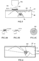
- the penetration length ⁇ of the evanescent waves OE is not constant over the entire surface S, but depends on the angle of incidence of the light rays; it therefore varies as a function of the distance from the vertical of the EL device.
- the figure 3C shows penetration iso-length curves forming circles around the opaque mask MO.
- the simplest way to obtain such a result is to replace the non-directional transmitter of the figure 2 by an ELD directional light emitting device (for example a super luminescent diode or a semiconductor laser) whose emission diagram has a maximum in a direction inclined with respect to the normal to the surface S; preferably, this direction forms with the normal to the surface S an angle greater than the limit angle.
- an ELD directional light emitting device for example a super luminescent diode or a semiconductor laser
- the emission diagram has a maximum in a direction inclined with respect to the normal to the surface S; preferably, this direction forms with the normal to the surface S an angle greater than the limit angle.
- the opaque mask MP can be omitted.
- the figure 5 illustrates a variant in which several directional light emitting devices ELD1, ELD2 are arranged one beside the other. These devices present emission diagrams having maxima in different directions, so as to define on the surface S of the substrate regions characterized by different penetration lengths of evanescent waves, as has been described with reference to figures 3A - 3C .
- Amplification of the evanescent wave generated in the ambient medium MA can also be obtained by trapping the excitation light radiation in a planar waveguide on the surface of the substrate. SB.
- a first transparent layer C1, of thickness e c1 and refractive index n c1 covers the surface S of the substrate SB;
- a second transparent layer C2 of thickness e c2 and refractive index n c2 is arranged above the first layer, in contact with the ambient medium.
- the thicknesses e c1 and e c2 do not exceed the wavelength of the light radiation emitted by the light emitting device (not shown) contained in the volume of the substrate.
- the layer C2 is directly in contact with the ambient medium MA and the sample to be observed, without the interposition of a microscope slide separated from the substrate.
- the refractive index n c1 of the first transparent layer is lower than that, n s , of the substrate: n c1 ⁇ n s ; consequently there is a limit angle such that the light rays coming from the substrate and arriving at its surface S with an angle of incidence greater than this limit angle undergo a total internal reflection.
- an evanescent wave OE1 is generated in the layer C1.
- the refractive index n c2 of the second transparent layer is greater both than that of the first transparent layer and that, n 1 , of the ambient medium: n c2 > n c1 ; n c2 > n 1 .
- the second transparent layer constitutes a planar wave guide.
- the evanescent wave OE1 generated in the first transparent layer excites a guide mode MG of this guide, which causes the appearance of an evanescent wave OE in the ambient medium - as in the other embodiments.
- the figure 6B is a graph representing, on a logarithmic scale, the intensity of the evanescent field as a function of the angle of incidence ⁇ and the wavelength ⁇ , for a TE polarization (electric field perpendicular to the plane of incidence). It can be noted that the intensification of the evanescent field occurs only at a determined angle of incidence, a function of the wavelength.
- the figure 6C shows the normalized intensity spatial profile (relative to the incident intensity) I N of the evanescent field, as a function of the distance z from the surface of the layer C2, for an optimal angle of incidence, equal to 64.2 °.
- the penetration length is of the order of 110 nm.
- CM a thin metallic layer
- LM a few nanometers or tens of nanometers
- S of the substrate if a separate microscope slide is not present.
- the simple embodiment of the figure 2 does not make it possible to obtain a uniform illumination (more precisely, an excitation of evanescent waves), since the light rays incident on the surface S come from a single direction.
- the useful region of the surface S, where the sample to be observed is to be positioned, is located in the vicinity of this axis.
- an ELA annular emitting device - for example a custom-made light-emitting diode - with an opaque MOA mask in the shape of a circular crown.
- the sample may contain several types of fluorophores, having different excitation wavelengths.
- a lighting device according to an embodiment of the invention can then advantageously comprise a plurality of light emitting devices, having different emission wavelengths, adapted to excite the fluorescence of respective fluorophores. These devices can be activated simultaneously or in sequence.
- the figure 9 illustrates an embodiment of the invention comprising three of these light emitting devices ELa, ELb, ELc, arranged symmetrically around an axis AS and each provided with a respective opaque mask MO1, MO2, MO3.
Landscapes
- Physics & Mathematics (AREA)
- General Physics & Mathematics (AREA)
- Health & Medical Sciences (AREA)
- Chemical & Material Sciences (AREA)
- Analytical Chemistry (AREA)
- General Health & Medical Sciences (AREA)
- Nuclear Medicine, Radiotherapy & Molecular Imaging (AREA)
- Optics & Photonics (AREA)
- Life Sciences & Earth Sciences (AREA)
- Biochemistry (AREA)
- Immunology (AREA)
- Pathology (AREA)
- Radiology & Medical Imaging (AREA)
- Microscoopes, Condenser (AREA)
- Investigating, Analyzing Materials By Fluorescence Or Luminescence (AREA)
Claims (16)
- Beleuchtungsvorrichtung für Fluoreszenzmikroskopie mit abklingender Welle, Folgendes beinhaltend:- ein Substrat (SB), welches für Licht in mindestens einem Spektralband transparent ist und in dem Spektralband einen Brechungsindex aufweist, welcher denjenigen von Wasser überschreitet;- mindestens eine Lichtemissionsvorrichtung (EL), welche innerhalb des Substrates angeordnet und geeignet ist, um eine Lichtstrahlung in dem Spektralbereich in Richtung einer Oberfläche (S) des Substrates auszusenden, wobei die Lichtemissionsvorrichtung so angeordnet ist, dass mindestens ein Teil der Strahlung die Oberfläche mit einem Einfallwinkel erreicht, welcher größer als oder gleich einem inneren Totalreflexions-Grenzwinkel für eine Schnittstelle zwischen dem Substrat und Wasser ist; und- mindestens eine undurchsichtige Maske (MO), welche innerhalb des Substrates oder an dessen Oberfläche in einer Weise angeordnet ist, dass sie einen Teil der Strahlung abfängt, welche bei Nichtvorhandensein der Maske die Oberfläche mit einem Einfallwinkel erreichen würde, welcher kleiner als der Grenzwinkel ist.
- Vorrichtung nach Anspruch 1, bei welcher die oder mindestens eine Lichtemissionsvorrichtung (ELD, ELD1, ELD2) eine Lichtemission vom direktionalen Typ aufweist, mit einem Emissionsdiagramm, welches ein Maximum in einer Richtung schräg in Bezug auf die Oberfläche des Substrates aufweist.
- Vorrichtung nach Anspruch 2, beinhaltend eine Vielzahl von solchen Lichtemissionsvorrichtungen (ELD1, ELD2), welche Lichtemissionen vom direktionalen Typ aufweisen, mit Emissionsdiagrammen, welche Maxima in jeweiligen voneinander unterschiedlichen Richtungen schräg in Bezug auf die Oberfläche des Substrates aufweisen.
- Vorrichtung nach einem der vorhergehenden Ansprüche, Folgendes beinhaltend:- entweder eine Vielzahl von solchen Lichtemissionsvorrichtungen (EL1, EL2, EL3), welche symmetrisch um eine Achse (AS) senkrecht zur Oberfläche des Substrates angeordnet ist;- oder eine Lichtemissionsvorrichtung (ELA) in Form eines Rings.
- Vorrichtung nach einem der vorhergehenden Ansprüche, beinhaltend eine Vielzahl von solchen Lichtemissionsvorrichtungen (ELa, ELb, ELc), welche geeignet ist, die Lichtstrahlung in unterschiedlichen Teilen des Spektralbandes auszusenden.
- Vorrichtung nach einem der vorhergehenden Ansprüche, außerdem Folgendes beinhaltend:- eine erste transparente Schicht (C1), welche an der Oberfläche des Substrates angeordnet ist und einen Brechungsindex unterhalb desjenigen des Substrates aufweist, sodass mindestens ein Teil der Lichtstrahlung, welche durch die Lichtemissionsvorrichtung(en) ausgesendet wird, eine Schnittstelle zwischen dem Substrat und der ersten transparenten Schicht mit einem Einfallwinkel erreicht, welcher größer als oder gleich einem inneren Totalreflexions-Grenzwinkel für diese Schnittstelle ist; und- eine zweite transparente Schicht (C2), welche an der dem Substrat abgewandten Oberfläche der ersten transparenten Schicht angeordnet ist, welche einen Brechungsindex aufweist, welche denjenigen der ersten Schicht überschreitet;
wobei die erste und die zweite Schicht geringere Dicken als mindestens eine Wellenlänge der durch die Lichtemissionsvorrichtung(en) ausgesandten Lichtstrahlung aufweisen. - Vorrichtung nach einem der vorhergehenden Ansprüche, zudem beinhaltend eine Metallschicht (CM), welche an ihrer durch die Lichtemissionsvorrichtung(en) beleuchteten Oberfläche abgelagert ist.
- Fluoreszenzmikroskopiesystem mit abklingender Welle, Folgendes beinhaltend:- eine Beleuchtungsvorrichtung nach einem der vorhergehenden Ansprüche; und- ein Mikroskopobjektiv (OBJ), welches angeordnet ist, um eine Oberfläche (S) der Beleuchtungsvorrichtung oder einen Mikroskop-Objektträger, welcher auf der Oberfläche abgelegt ist, zu beobachten, und welches eine zu der Oberfläche rechtwinklige und in Bezug auf die Lichtemissionsvorrichtung(en) der Beleuchtungsvorrichtung versetzte optische Achse (AO) aufweist.
- Beleuchtungsverfahren für Fluoreszenzmikroskopie mit abklingender Welle, folgende Schritte beinhaltend:- Inkontaktbringen eines Substrates (SB), welches für Licht in mindestens einem Spektralband transparent ist, mit einem Medium (MA), welches in dem Spektralband einen Brechungsindex aufweist, welcher denjenigen des Substrates unterschreitet;- Aktivieren einer Lichtemissionsvorrichtung (EL), welche innerhalb des transparenten Substrates angeordnet ist, damit diese eine Lichtstrahlung in dem Spektralbereich in Richtung einer Oberfläche (S) des Substrates aussendet, wobei die Lichtemissionsvorrichtung so angeordnet ist, dass mindestens ein Teil der Strahlung die Oberfläche mit einem Einfallwinkel erreicht, welcher größer als oder gleich einem inneren Totalreflexions-Grenzwinkel für eine Schnittstelle zwischen dem Substrat und dem optischen Medium ist;
wodurch abklingende Wellen (OE) an der Oberfläche des Substrates erzeugt werden. - Verfahren nach Anspruch 9, bei welchem mindestens eine undurchsichtige Maske (MO) innerhalb des Substrates oder an dessen Oberfläche in einer Weise angeordnet ist, dass sie einen Teil der Strahlung abfängt, welche bei Nichtvorhandensein der Maske die Oberfläche mit einem Einfallwinkel erreichen würde, welcher kleiner als der Grenzwinkel ist.
- Verfahren nach einem der Ansprüche 9 oder 10, bei welchem das Medium wässrig ist.
- Verfahren nach einem der Ansprüche 9 bis 11, bei welchem die oder mindestens eine Lichtemissionsvorrichtung eine Lichtemission vom direktionalen Typ aufweist, mit einem Emissionsdiagramm, welches ein Maximum in einer Richtung schräg in Bezug auf die Oberfläche des Substrates aufweist.
- Verfahren nach einem der Ansprüche 9 bis 12, bei welchem:- eine erste transparente Schicht (C1) an der Oberfläche des Substrates angeordnet ist und einen Brechungsindex unterhalb desjenigen des Substrates aufweist, sodass mindestens ein Teil der Lichtstrahlung, welche durch die Lichtemissionsvorrichtung(en) ausgesendet wird, eine Schnittstelle Substrat - erste transparente Schicht mit einem Einfallwinkel erreicht, welcher größer als oder gleich einem inneren Totalreflexions-Grenzwinkel für diese Schnittstelle ist; und- eine zweite transparente Schicht (C2), an der dem Substrat abgewandten Oberfläche der ersten transparenten Schicht angeordnet ist, welche einen Brechungsindex aufweist, welche denjenigen der ersten Schicht überschreitet;
wobei die erste und die zweite Schicht geringere Dicken als mindestens eine Wellenlänge der durch die Lichtemissionsvorrichtung(en) ausgesandten Lichtstrahlung aufweisen. - Verfahren nach einem der Ansprüche 9 bis 13, bei welchem eine Metallschicht (CM) an der Oberfläche des Substrates oder in dessen Nähe angeordnet ist, sodass Oberflächenplasmonen durch die abklingenden Wellen angeregt werden.
- Verfahren nach einem der Ansprüche 9 bis 14, bei welchem eine Probe (ECH), beinhaltend mindestens ein Fluorophor, in Kontakt mit der Oberfläche des Substrates oder in dessen Nähe gebracht wird, sodass eine Fluoreszenzemission des Fluorophors durch die abklingenden Wellen angeregt wird, oder durch abklingende Wellen, welche den Oberflächenplasmonen zugeordnet sind, und bei welchem mindestens ein Fluoreszenzbild der Probe mithilfe eines Mikroskopobjektivs erfasst wird.
- Verfahren nach Anspruch 15, bei welchem:- die Lichtemissionsvorrichtung(en) so angeordnet ist/sind, dass die abklingenden Wellen, unterschiedliche Penetrationslängen übereinstimmend mit unterschiedlichen Punkten der Oberfläche des Substrates aufweisen;- das Substrat in Bezug auf die Probe bewegt wird und eine Vielzahl von Fluoreszenzbildern für eine Vielzahl unterschiedlicher relativer Positionen zwischen der Probe und dem Substrat in einer Weise erfasst wird, dass ein gleicher Punkt der Probe abklingenden Wellen unterschiedlicher Penetrationslänge gegenüber exponiert wird;- wobei das Verfahren außerdem einen Schritt der Rekonstruktion eines dreidimensionalen Bildes einer Verteilung der Fluorophore innerhalb der Probe anhand der Fluoreszenzbilder beinhaltet.
Applications Claiming Priority (2)
| Application Number | Priority Date | Filing Date | Title |
|---|---|---|---|
| FR1654885A FR3051921B1 (fr) | 2016-05-31 | 2016-05-31 | Dispositif et procede d'eclairage pour microscopie de fluorescence a onde evanescente |
| PCT/EP2017/062440 WO2017207360A1 (fr) | 2016-05-31 | 2017-05-23 | Dispositif et procede d'eclairage pour microscopie de fluorescence a onde evanescente |
Publications (2)
| Publication Number | Publication Date |
|---|---|
| EP3465320A1 EP3465320A1 (de) | 2019-04-10 |
| EP3465320B1 true EP3465320B1 (de) | 2020-05-20 |
Family
ID=56990519
Family Applications (1)
| Application Number | Title | Priority Date | Filing Date |
|---|---|---|---|
| EP17726253.2A Active EP3465320B1 (de) | 2016-05-31 | 2017-05-23 | Vorrichtung und verfahren zur bereitstellung von beleuchtung für fluoreszenzmikroskopie mit interner totalreflexion |
Country Status (5)
| Country | Link |
|---|---|
| US (1) | US11047799B2 (de) |
| EP (1) | EP3465320B1 (de) |
| JP (1) | JP6918023B2 (de) |
| FR (1) | FR3051921B1 (de) |
| WO (1) | WO2017207360A1 (de) |
Families Citing this family (1)
| Publication number | Priority date | Publication date | Assignee | Title |
|---|---|---|---|---|
| US12164097B2 (en) * | 2020-02-24 | 2024-12-10 | Massachusetts Institute Of Technology | Bragg light source for dark-field imaging devices |
Family Cites Families (15)
| Publication number | Priority date | Publication date | Assignee | Title |
|---|---|---|---|---|
| JPH1166928A (ja) * | 1997-08-22 | 1999-03-09 | Bridgestone Corp | 線状発光体 |
| CN100385232C (zh) * | 1998-08-26 | 2008-04-30 | 医药及科学传感器公司 | 基于光学的感测装置 |
| JP2000264744A (ja) | 1999-03-12 | 2000-09-26 | Nissan Motor Co Ltd | カーボン/カーボン複合材からなる積層体の製造方法 |
| EP1425570B1 (de) * | 2001-09-11 | 2009-03-18 | Dublin City University | Sensoranordnung zur lumineszenzmessung |
| WO2004031743A1 (en) | 2002-10-07 | 2004-04-15 | The Secretary Of State For Defence | A waveguide structure |
| US7545496B2 (en) * | 2003-06-25 | 2009-06-09 | Koninklijke Philips Electronics N.V. | Support with a surface structure for sensitive evanescent-field detection |
| JP5087745B2 (ja) | 2005-09-26 | 2012-12-05 | 国立大学法人浜松医科大学 | 複数の観察手法を用いた顕微鏡細胞観察・検査システム |
| JP2008209726A (ja) | 2007-02-27 | 2008-09-11 | Olympus Corp | 照明装置 |
| KR20100124737A (ko) | 2008-02-01 | 2010-11-29 | 레어 라이트, 인크. | 임계 주변 반사 분광법을 위한 방법, 장치 및 키트 |
| JP5180703B2 (ja) * | 2008-06-27 | 2013-04-10 | 富士フイルム株式会社 | 検出方法、検出用試料セルおよび検出用キット |
| FR2943428B1 (fr) * | 2009-03-20 | 2011-05-13 | Univ Paris Diderot Paris 7 | Dispositif de microscopie de fluorescence et methode d'observation associe |
| JP5328915B2 (ja) * | 2009-07-03 | 2013-10-30 | 株式会社日立製作所 | 高感度蛍光検出デバイス |
| FR2966937B1 (fr) * | 2010-10-28 | 2012-12-28 | Univ Paris Diderot Paris 7 | Methode d'observation de l'emission de lumiere d'un echantillon par microscopie optique dynamique |
| CN102410996A (zh) | 2011-08-26 | 2012-04-11 | 上海交通大学 | 基于全反射的平面并行荧光生物检测芯片及其制备方法 |
| US9500847B2 (en) * | 2012-10-12 | 2016-11-22 | Spectral Applied Research Inc. | Total internal reflectance fluorescence (TIRF) microscopy across multiple wavelengths simultaneously |
-
2016
- 2016-05-31 FR FR1654885A patent/FR3051921B1/fr not_active Expired - Fee Related
-
2017
- 2017-05-23 JP JP2018562653A patent/JP6918023B2/ja active Active
- 2017-05-23 EP EP17726253.2A patent/EP3465320B1/de active Active
- 2017-05-23 US US16/302,055 patent/US11047799B2/en active Active
- 2017-05-23 WO PCT/EP2017/062440 patent/WO2017207360A1/fr not_active Ceased
Non-Patent Citations (1)
| Title |
|---|
| None * |
Also Published As
| Publication number | Publication date |
|---|---|
| US11047799B2 (en) | 2021-06-29 |
| WO2017207360A1 (fr) | 2017-12-07 |
| FR3051921A1 (fr) | 2017-12-01 |
| JP6918023B2 (ja) | 2021-08-11 |
| FR3051921B1 (fr) | 2018-06-01 |
| JP2019522814A (ja) | 2019-08-15 |
| EP3465320A1 (de) | 2019-04-10 |
| US20190285547A1 (en) | 2019-09-19 |
Similar Documents
| Publication | Publication Date | Title |
|---|---|---|
| EP3270232B1 (de) | Beobachtungsvorrichtung für eine probe | |
| EP4052073B1 (de) | Diffraktives optisches element mit einer metaoberfläche für die tirf-mikroskopie | |
| EP3397944B1 (de) | Vorrichtung und verfahren zur bimodalen beobachtung eines objekts | |
| EP3371574B1 (de) | Vorrichtung und verfahren zur beobachtung eines objekts mittels linsenfreier abbildung | |
| EP4016053A1 (de) | Optische komponente für eine interferometrische bildgebungsvorrichtung | |
| EP3465320B1 (de) | Vorrichtung und verfahren zur bereitstellung von beleuchtung für fluoreszenzmikroskopie mit interner totalreflexion | |
| EP2710351B1 (de) | Biochip-vorrichtung | |
| EP3054281A1 (de) | Vorrichtung zum messen eines von einer probe rückgestreuten optischen signals | |
| WO2009144187A1 (fr) | Dispositif de piégeage de particules | |
| WO2017220919A1 (fr) | Reflecteur optique resonant a multiples couches minces de materiaux dielectriques, capteur optique, dispositif d'amplification laser comportant un tel reflecteur et procedes de fabrication correspondants | |
| EP3751258B1 (de) | Vorrichtung und verfahren zur beobachtung einer fluoreszenten probe | |
| WO2020128105A1 (fr) | Détecteur optique de particules | |
| FR2943428A1 (fr) | Dispositif de microscopie de fluorescence et methode d'observation associe | |
| EP3545362B1 (de) | Verfahren zur herstellung eines hochauflösenden bildes durch linsenlose bildgebung | |
| WO2020230051A1 (fr) | Dispositif de creation d'un champ evanescent a motifs sur une surface et procede associe | |
| EP3575774B1 (de) | Verfahren zur beobachtung von teilchen, insbesondere teilchen im submikrometerbereich | |
| WO2023025842A1 (fr) | Lame optique biocompatible destinee a la microscopie a reflexion totale interne et systeme d'imagerie microscopique comportant une telle lame | |
| FR2924855A1 (fr) | Procede de positionnement de particule dans une zone cible et dispositif associe | |
| FR2893131A1 (fr) | Procede de detection de nanoparticules et ses applications | |
| WO2024074241A1 (fr) | Substrat optique à antennes intégrées et spectomètre le comprenant | |
| FR2979689A1 (fr) | Dispositif d'eclairage d'un objet, a source de lumiere munie d'un organe de prelevement d'une portion de la lumiere, application a la mesure des variations de flux de la source | |
| FR3004814A1 (fr) | Systeme de detection optique comportant un dispositif de collection de lumiere | |
| Jozefowski et al. | Leakage radiation spectroscopy of organic nanofibers on metal films: evidence for exciton-surface plasmon polariton interaction |
Legal Events
| Date | Code | Title | Description |
|---|---|---|---|
| STAA | Information on the status of an ep patent application or granted ep patent |
Free format text: STATUS: UNKNOWN |
|
| STAA | Information on the status of an ep patent application or granted ep patent |
Free format text: STATUS: THE INTERNATIONAL PUBLICATION HAS BEEN MADE |
|
| PUAI | Public reference made under article 153(3) epc to a published international application that has entered the european phase |
Free format text: ORIGINAL CODE: 0009012 |
|
| STAA | Information on the status of an ep patent application or granted ep patent |
Free format text: STATUS: REQUEST FOR EXAMINATION WAS MADE |
|
| 17P | Request for examination filed |
Effective date: 20181122 |
|
| AK | Designated contracting states |
Kind code of ref document: A1 Designated state(s): AL AT BE BG CH CY CZ DE DK EE ES FI FR GB GR HR HU IE IS IT LI LT LU LV MC MK MT NL NO PL PT RO RS SE SI SK SM TR |
|
| AX | Request for extension of the european patent |
Extension state: BA ME |
|
| RIN1 | Information on inventor provided before grant (corrected) |
Inventor name: LEFEBVRE, DENIS Inventor name: BRUNSTEIN, MAIA Inventor name: BOUCHOULE, SOPHIE Inventor name: GIACOMOTTI, ALEJANDRO Inventor name: DAMILANO, BENJAMIN Inventor name: CATTONI, ANDREA |
|
| DAV | Request for validation of the european patent (deleted) | ||
| DAX | Request for extension of the european patent (deleted) | ||
| GRAP | Despatch of communication of intention to grant a patent |
Free format text: ORIGINAL CODE: EPIDOSNIGR1 |
|
| STAA | Information on the status of an ep patent application or granted ep patent |
Free format text: STATUS: GRANT OF PATENT IS INTENDED |
|
| INTG | Intention to grant announced |
Effective date: 20191218 |
|
| GRAS | Grant fee paid |
Free format text: ORIGINAL CODE: EPIDOSNIGR3 |
|
| GRAA | (expected) grant |
Free format text: ORIGINAL CODE: 0009210 |
|
| STAA | Information on the status of an ep patent application or granted ep patent |
Free format text: STATUS: THE PATENT HAS BEEN GRANTED |
|
| AK | Designated contracting states |
Kind code of ref document: B1 Designated state(s): AL AT BE BG CH CY CZ DE DK EE ES FI FR GB GR HR HU IE IS IT LI LT LU LV MC MK MT NL NO PL PT RO RS SE SI SK SM TR |
|
| REG | Reference to a national code |
Ref country code: GB Ref legal event code: FG4D Free format text: NOT ENGLISH |
|
| REG | Reference to a national code |
Ref country code: CH Ref legal event code: EP |
|
| REG | Reference to a national code |
Ref country code: DE Ref legal event code: R096 Ref document number: 602017017037 Country of ref document: DE |
|
| REG | Reference to a national code |
Ref country code: AT Ref legal event code: REF Ref document number: 1272971 Country of ref document: AT Kind code of ref document: T Effective date: 20200615 |
|
| REG | Reference to a national code |
Ref country code: CH Ref legal event code: NV Representative=s name: SERVOPATENT GMBH, CH |
|
| REG | Reference to a national code |
Ref country code: LT Ref legal event code: MG4D |
|
| REG | Reference to a national code |
Ref country code: NL Ref legal event code: MP Effective date: 20200520 |
|
| PG25 | Lapsed in a contracting state [announced via postgrant information from national office to epo] |
Ref country code: PT Free format text: LAPSE BECAUSE OF FAILURE TO SUBMIT A TRANSLATION OF THE DESCRIPTION OR TO PAY THE FEE WITHIN THE PRESCRIBED TIME-LIMIT Effective date: 20200921 Ref country code: IS Free format text: LAPSE BECAUSE OF FAILURE TO SUBMIT A TRANSLATION OF THE DESCRIPTION OR TO PAY THE FEE WITHIN THE PRESCRIBED TIME-LIMIT Effective date: 20200920 Ref country code: FI Free format text: LAPSE BECAUSE OF FAILURE TO SUBMIT A TRANSLATION OF THE DESCRIPTION OR TO PAY THE FEE WITHIN THE PRESCRIBED TIME-LIMIT Effective date: 20200520 Ref country code: NO Free format text: LAPSE BECAUSE OF FAILURE TO SUBMIT A TRANSLATION OF THE DESCRIPTION OR TO PAY THE FEE WITHIN THE PRESCRIBED TIME-LIMIT Effective date: 20200820 Ref country code: GR Free format text: LAPSE BECAUSE OF FAILURE TO SUBMIT A TRANSLATION OF THE DESCRIPTION OR TO PAY THE FEE WITHIN THE PRESCRIBED TIME-LIMIT Effective date: 20200821 Ref country code: SE Free format text: LAPSE BECAUSE OF FAILURE TO SUBMIT A TRANSLATION OF THE DESCRIPTION OR TO PAY THE FEE WITHIN THE PRESCRIBED TIME-LIMIT Effective date: 20200520 Ref country code: LT Free format text: LAPSE BECAUSE OF FAILURE TO SUBMIT A TRANSLATION OF THE DESCRIPTION OR TO PAY THE FEE WITHIN THE PRESCRIBED TIME-LIMIT Effective date: 20200520 |
|
| PG25 | Lapsed in a contracting state [announced via postgrant information from national office to epo] |
Ref country code: BG Free format text: LAPSE BECAUSE OF FAILURE TO SUBMIT A TRANSLATION OF THE DESCRIPTION OR TO PAY THE FEE WITHIN THE PRESCRIBED TIME-LIMIT Effective date: 20200820 Ref country code: HR Free format text: LAPSE BECAUSE OF FAILURE TO SUBMIT A TRANSLATION OF THE DESCRIPTION OR TO PAY THE FEE WITHIN THE PRESCRIBED TIME-LIMIT Effective date: 20200520 Ref country code: LV Free format text: LAPSE BECAUSE OF FAILURE TO SUBMIT A TRANSLATION OF THE DESCRIPTION OR TO PAY THE FEE WITHIN THE PRESCRIBED TIME-LIMIT Effective date: 20200520 Ref country code: RS Free format text: LAPSE BECAUSE OF FAILURE TO SUBMIT A TRANSLATION OF THE DESCRIPTION OR TO PAY THE FEE WITHIN THE PRESCRIBED TIME-LIMIT Effective date: 20200520 |
|
| REG | Reference to a national code |
Ref country code: AT Ref legal event code: MK05 Ref document number: 1272971 Country of ref document: AT Kind code of ref document: T Effective date: 20200520 |
|
| PG25 | Lapsed in a contracting state [announced via postgrant information from national office to epo] |
Ref country code: AL Free format text: LAPSE BECAUSE OF FAILURE TO SUBMIT A TRANSLATION OF THE DESCRIPTION OR TO PAY THE FEE WITHIN THE PRESCRIBED TIME-LIMIT Effective date: 20200520 Ref country code: NL Free format text: LAPSE BECAUSE OF FAILURE TO SUBMIT A TRANSLATION OF THE DESCRIPTION OR TO PAY THE FEE WITHIN THE PRESCRIBED TIME-LIMIT Effective date: 20200520 |
|
| PG25 | Lapsed in a contracting state [announced via postgrant information from national office to epo] |
Ref country code: AT Free format text: LAPSE BECAUSE OF FAILURE TO SUBMIT A TRANSLATION OF THE DESCRIPTION OR TO PAY THE FEE WITHIN THE PRESCRIBED TIME-LIMIT Effective date: 20200520 Ref country code: EE Free format text: LAPSE BECAUSE OF FAILURE TO SUBMIT A TRANSLATION OF THE DESCRIPTION OR TO PAY THE FEE WITHIN THE PRESCRIBED TIME-LIMIT Effective date: 20200520 Ref country code: SM Free format text: LAPSE BECAUSE OF FAILURE TO SUBMIT A TRANSLATION OF THE DESCRIPTION OR TO PAY THE FEE WITHIN THE PRESCRIBED TIME-LIMIT Effective date: 20200520 Ref country code: DK Free format text: LAPSE BECAUSE OF FAILURE TO SUBMIT A TRANSLATION OF THE DESCRIPTION OR TO PAY THE FEE WITHIN THE PRESCRIBED TIME-LIMIT Effective date: 20200520 Ref country code: CZ Free format text: LAPSE BECAUSE OF FAILURE TO SUBMIT A TRANSLATION OF THE DESCRIPTION OR TO PAY THE FEE WITHIN THE PRESCRIBED TIME-LIMIT Effective date: 20200520 Ref country code: IT Free format text: LAPSE BECAUSE OF FAILURE TO SUBMIT A TRANSLATION OF THE DESCRIPTION OR TO PAY THE FEE WITHIN THE PRESCRIBED TIME-LIMIT Effective date: 20200520 Ref country code: ES Free format text: LAPSE BECAUSE OF FAILURE TO SUBMIT A TRANSLATION OF THE DESCRIPTION OR TO PAY THE FEE WITHIN THE PRESCRIBED TIME-LIMIT Effective date: 20200520 Ref country code: RO Free format text: LAPSE BECAUSE OF FAILURE TO SUBMIT A TRANSLATION OF THE DESCRIPTION OR TO PAY THE FEE WITHIN THE PRESCRIBED TIME-LIMIT Effective date: 20200520 |
|
| REG | Reference to a national code |
Ref country code: DE Ref legal event code: R097 Ref document number: 602017017037 Country of ref document: DE |
|
| PG25 | Lapsed in a contracting state [announced via postgrant information from national office to epo] |
Ref country code: PL Free format text: LAPSE BECAUSE OF FAILURE TO SUBMIT A TRANSLATION OF THE DESCRIPTION OR TO PAY THE FEE WITHIN THE PRESCRIBED TIME-LIMIT Effective date: 20200520 Ref country code: MC Free format text: LAPSE BECAUSE OF FAILURE TO SUBMIT A TRANSLATION OF THE DESCRIPTION OR TO PAY THE FEE WITHIN THE PRESCRIBED TIME-LIMIT Effective date: 20200520 Ref country code: SK Free format text: LAPSE BECAUSE OF FAILURE TO SUBMIT A TRANSLATION OF THE DESCRIPTION OR TO PAY THE FEE WITHIN THE PRESCRIBED TIME-LIMIT Effective date: 20200520 |
|
| PLBE | No opposition filed within time limit |
Free format text: ORIGINAL CODE: 0009261 |
|
| STAA | Information on the status of an ep patent application or granted ep patent |
Free format text: STATUS: NO OPPOSITION FILED WITHIN TIME LIMIT |
|
| PG25 | Lapsed in a contracting state [announced via postgrant information from national office to epo] |
Ref country code: LU Free format text: LAPSE BECAUSE OF NON-PAYMENT OF DUE FEES Effective date: 20200523 |
|
| 26N | No opposition filed |
Effective date: 20210223 |
|
| PG25 | Lapsed in a contracting state [announced via postgrant information from national office to epo] |
Ref country code: IE Free format text: LAPSE BECAUSE OF NON-PAYMENT OF DUE FEES Effective date: 20200523 |
|
| PG25 | Lapsed in a contracting state [announced via postgrant information from national office to epo] |
Ref country code: SI Free format text: LAPSE BECAUSE OF FAILURE TO SUBMIT A TRANSLATION OF THE DESCRIPTION OR TO PAY THE FEE WITHIN THE PRESCRIBED TIME-LIMIT Effective date: 20200520 |
|
| PG25 | Lapsed in a contracting state [announced via postgrant information from national office to epo] |
Ref country code: TR Free format text: LAPSE BECAUSE OF FAILURE TO SUBMIT A TRANSLATION OF THE DESCRIPTION OR TO PAY THE FEE WITHIN THE PRESCRIBED TIME-LIMIT Effective date: 20200520 Ref country code: MT Free format text: LAPSE BECAUSE OF FAILURE TO SUBMIT A TRANSLATION OF THE DESCRIPTION OR TO PAY THE FEE WITHIN THE PRESCRIBED TIME-LIMIT Effective date: 20200520 Ref country code: CY Free format text: LAPSE BECAUSE OF FAILURE TO SUBMIT A TRANSLATION OF THE DESCRIPTION OR TO PAY THE FEE WITHIN THE PRESCRIBED TIME-LIMIT Effective date: 20200520 |
|
| PG25 | Lapsed in a contracting state [announced via postgrant information from national office to epo] |
Ref country code: MK Free format text: LAPSE BECAUSE OF FAILURE TO SUBMIT A TRANSLATION OF THE DESCRIPTION OR TO PAY THE FEE WITHIN THE PRESCRIBED TIME-LIMIT Effective date: 20200520 |
|
| PGFP | Annual fee paid to national office [announced via postgrant information from national office to epo] |
Ref country code: DE Payment date: 20250626 Year of fee payment: 9 |
|
| PGFP | Annual fee paid to national office [announced via postgrant information from national office to epo] |
Ref country code: GB Payment date: 20250528 Year of fee payment: 9 |
|
| PGFP | Annual fee paid to national office [announced via postgrant information from national office to epo] |
Ref country code: BE Payment date: 20250527 Year of fee payment: 9 |
|
| PGFP | Annual fee paid to national office [announced via postgrant information from national office to epo] |
Ref country code: FR Payment date: 20250528 Year of fee payment: 9 |
|
| PGFP | Annual fee paid to national office [announced via postgrant information from national office to epo] |
Ref country code: CH Payment date: 20250627 Year of fee payment: 9 |