EP3650908B1 - Dispositif optique - Google Patents
Dispositif optique Download PDFInfo
- Publication number
- EP3650908B1 EP3650908B1 EP18827624.0A EP18827624A EP3650908B1 EP 3650908 B1 EP3650908 B1 EP 3650908B1 EP 18827624 A EP18827624 A EP 18827624A EP 3650908 B1 EP3650908 B1 EP 3650908B1
- Authority
- EP
- European Patent Office
- Prior art keywords
- mirror
- unit
- axis direction
- optical
- light
- Prior art date
- Legal status (The legal status is an assumption and is not a legal conclusion. Google has not performed a legal analysis and makes no representation as to the accuracy of the status listed.)
- Active
Links
Images





Classifications
-
- G—PHYSICS
- G01—MEASURING; TESTING
- G01B—MEASURING LENGTH, THICKNESS OR SIMILAR LINEAR DIMENSIONS; MEASURING ANGLES; MEASURING AREAS; MEASURING IRREGULARITIES OF SURFACES OR CONTOURS
- G01B9/00—Measuring instruments characterised by the use of optical techniques
- G01B9/02—Interferometers
- G01B9/02049—Interferometers characterised by particular mechanical design details
- G01B9/02051—Integrated design, e.g. on-chip or monolithic
-
- B—PERFORMING OPERATIONS; TRANSPORTING
- B81—MICROSTRUCTURAL TECHNOLOGY
- B81B—MICROSTRUCTURAL DEVICES OR SYSTEMS, e.g. MICROMECHANICAL DEVICES
- B81B3/00—Devices comprising flexible or deformable elements, e.g. comprising elastic tongues or membranes
-
- B—PERFORMING OPERATIONS; TRANSPORTING
- B81—MICROSTRUCTURAL TECHNOLOGY
- B81B—MICROSTRUCTURAL DEVICES OR SYSTEMS, e.g. MICROMECHANICAL DEVICES
- B81B3/00—Devices comprising flexible or deformable elements, e.g. comprising elastic tongues or membranes
- B81B3/0018—Structures acting upon the moving or flexible element for transforming energy into mechanical movement or vice versa, i.e. actuators, sensors, generators
- B81B3/0021—Transducers for transforming electrical into mechanical energy or vice versa
-
- B—PERFORMING OPERATIONS; TRANSPORTING
- B81—MICROSTRUCTURAL TECHNOLOGY
- B81B—MICROSTRUCTURAL DEVICES OR SYSTEMS, e.g. MICROMECHANICAL DEVICES
- B81B3/00—Devices comprising flexible or deformable elements, e.g. comprising elastic tongues or membranes
- B81B3/0064—Constitution or structural means for improving or controlling the physical properties of a device
- B81B3/0067—Mechanical properties
- B81B3/007—For controlling stiffness, e.g. ribs
-
- B—PERFORMING OPERATIONS; TRANSPORTING
- B81—MICROSTRUCTURAL TECHNOLOGY
- B81B—MICROSTRUCTURAL DEVICES OR SYSTEMS, e.g. MICROMECHANICAL DEVICES
- B81B7/00—Microstructural systems ; Auxiliary parts of microstructural devices or systems
- B81B7/02—Microstructural systems ; Auxiliary parts of microstructural devices or systems containing distinct electrical or optical devices of particular relevance for their function, e.g. microelectro-mechanical systems [MEMS]
-
- G—PHYSICS
- G01—MEASURING; TESTING
- G01B—MEASURING LENGTH, THICKNESS OR SIMILAR LINEAR DIMENSIONS; MEASURING ANGLES; MEASURING AREAS; MEASURING IRREGULARITIES OF SURFACES OR CONTOURS
- G01B9/00—Measuring instruments characterised by the use of optical techniques
- G01B9/02—Interferometers
-
- G—PHYSICS
- G01—MEASURING; TESTING
- G01B—MEASURING LENGTH, THICKNESS OR SIMILAR LINEAR DIMENSIONS; MEASURING ANGLES; MEASURING AREAS; MEASURING IRREGULARITIES OF SURFACES OR CONTOURS
- G01B9/00—Measuring instruments characterised by the use of optical techniques
- G01B9/02—Interferometers
- G01B9/02049—Interferometers characterised by particular mechanical design details
-
- G—PHYSICS
- G01—MEASURING; TESTING
- G01J—MEASUREMENT OF INTENSITY, VELOCITY, SPECTRAL CONTENT, POLARISATION, PHASE OR PULSE CHARACTERISTICS OF INFRARED, VISIBLE OR ULTRAVIOLET LIGHT; COLORIMETRY; RADIATION PYROMETRY
- G01J3/00—Spectrometry; Spectrophotometry; Monochromators; Measuring colours
- G01J3/02—Details
- G01J3/0202—Mechanical elements; Supports for optical elements
-
- G—PHYSICS
- G01—MEASURING; TESTING
- G01J—MEASUREMENT OF INTENSITY, VELOCITY, SPECTRAL CONTENT, POLARISATION, PHASE OR PULSE CHARACTERISTICS OF INFRARED, VISIBLE OR ULTRAVIOLET LIGHT; COLORIMETRY; RADIATION PYROMETRY
- G01J3/00—Spectrometry; Spectrophotometry; Monochromators; Measuring colours
- G01J3/02—Details
- G01J3/0205—Optical elements not provided otherwise, e.g. optical manifolds, diffusers, windows
- G01J3/021—Optical elements not provided otherwise, e.g. optical manifolds, diffusers, windows using plane or convex mirrors, parallel phase plates, or particular reflectors
-
- G—PHYSICS
- G01—MEASURING; TESTING
- G01J—MEASUREMENT OF INTENSITY, VELOCITY, SPECTRAL CONTENT, POLARISATION, PHASE OR PULSE CHARACTERISTICS OF INFRARED, VISIBLE OR ULTRAVIOLET LIGHT; COLORIMETRY; RADIATION PYROMETRY
- G01J3/00—Spectrometry; Spectrophotometry; Monochromators; Measuring colours
- G01J3/02—Details
- G01J3/0205—Optical elements not provided otherwise, e.g. optical manifolds, diffusers, windows
- G01J3/0237—Adjustable, e.g. focussing
-
- G—PHYSICS
- G01—MEASURING; TESTING
- G01J—MEASUREMENT OF INTENSITY, VELOCITY, SPECTRAL CONTENT, POLARISATION, PHASE OR PULSE CHARACTERISTICS OF INFRARED, VISIBLE OR ULTRAVIOLET LIGHT; COLORIMETRY; RADIATION PYROMETRY
- G01J3/00—Spectrometry; Spectrophotometry; Monochromators; Measuring colours
- G01J3/02—Details
- G01J3/06—Scanning arrangements arrangements for order-selection
-
- G—PHYSICS
- G01—MEASURING; TESTING
- G01J—MEASUREMENT OF INTENSITY, VELOCITY, SPECTRAL CONTENT, POLARISATION, PHASE OR PULSE CHARACTERISTICS OF INFRARED, VISIBLE OR ULTRAVIOLET LIGHT; COLORIMETRY; RADIATION PYROMETRY
- G01J3/00—Spectrometry; Spectrophotometry; Monochromators; Measuring colours
- G01J3/02—Details
- G01J3/10—Arrangements of light sources specially adapted for spectrometry or colorimetry
- G01J3/108—Arrangements of light sources specially adapted for spectrometry or colorimetry for measurement in the infrared range
-
- G—PHYSICS
- G01—MEASURING; TESTING
- G01J—MEASUREMENT OF INTENSITY, VELOCITY, SPECTRAL CONTENT, POLARISATION, PHASE OR PULSE CHARACTERISTICS OF INFRARED, VISIBLE OR ULTRAVIOLET LIGHT; COLORIMETRY; RADIATION PYROMETRY
- G01J3/00—Spectrometry; Spectrophotometry; Monochromators; Measuring colours
- G01J3/12—Generating the spectrum; Monochromators
- G01J3/14—Generating the spectrum; Monochromators using refracting elements, e.g. prisms
-
- G—PHYSICS
- G01—MEASURING; TESTING
- G01J—MEASUREMENT OF INTENSITY, VELOCITY, SPECTRAL CONTENT, POLARISATION, PHASE OR PULSE CHARACTERISTICS OF INFRARED, VISIBLE OR ULTRAVIOLET LIGHT; COLORIMETRY; RADIATION PYROMETRY
- G01J3/00—Spectrometry; Spectrophotometry; Monochromators; Measuring colours
- G01J3/28—Investigating the spectrum
- G01J3/45—Interferometric spectrometry
-
- G—PHYSICS
- G02—OPTICS
- G02B—OPTICAL ELEMENTS, SYSTEMS OR APPARATUS
- G02B26/00—Optical devices or arrangements for the control of light using movable or deformable optical elements
- G02B26/08—Optical devices or arrangements for the control of light using movable or deformable optical elements for controlling the direction of light
- G02B26/0816—Optical devices or arrangements for the control of light using movable or deformable optical elements for controlling the direction of light by means of one or more reflecting elements
-
- G—PHYSICS
- G02—OPTICS
- G02B—OPTICAL ELEMENTS, SYSTEMS OR APPARATUS
- G02B26/00—Optical devices or arrangements for the control of light using movable or deformable optical elements
- G02B26/08—Optical devices or arrangements for the control of light using movable or deformable optical elements for controlling the direction of light
- G02B26/0816—Optical devices or arrangements for the control of light using movable or deformable optical elements for controlling the direction of light by means of one or more reflecting elements
- G02B26/0833—Optical devices or arrangements for the control of light using movable or deformable optical elements for controlling the direction of light by means of one or more reflecting elements the reflecting element being a micromechanical device, e.g. a MEMS mirror, DMD
-
- G—PHYSICS
- G02—OPTICS
- G02B—OPTICAL ELEMENTS, SYSTEMS OR APPARATUS
- G02B26/00—Optical devices or arrangements for the control of light using movable or deformable optical elements
- G02B26/08—Optical devices or arrangements for the control of light using movable or deformable optical elements for controlling the direction of light
- G02B26/0816—Optical devices or arrangements for the control of light using movable or deformable optical elements for controlling the direction of light by means of one or more reflecting elements
- G02B26/0833—Optical devices or arrangements for the control of light using movable or deformable optical elements for controlling the direction of light by means of one or more reflecting elements the reflecting element being a micromechanical device, e.g. a MEMS mirror, DMD
- G02B26/0841—Optical devices or arrangements for the control of light using movable or deformable optical elements for controlling the direction of light by means of one or more reflecting elements the reflecting element being a micromechanical device, e.g. a MEMS mirror, DMD the reflecting element being moved or deformed by electrostatic means
-
- G—PHYSICS
- G02—OPTICS
- G02B—OPTICAL ELEMENTS, SYSTEMS OR APPARATUS
- G02B27/00—Optical systems or apparatus not provided for by any of the groups G02B1/00 - G02B26/00, G02B30/00
- G02B27/10—Beam splitting or combining systems
- G02B27/14—Beam splitting or combining systems operating by reflection only
- G02B27/144—Beam splitting or combining systems operating by reflection only using partially transparent surfaces without spectral selectivity
-
- G—PHYSICS
- G02—OPTICS
- G02B—OPTICAL ELEMENTS, SYSTEMS OR APPARATUS
- G02B27/00—Optical systems or apparatus not provided for by any of the groups G02B1/00 - G02B26/00, G02B30/00
- G02B27/10—Beam splitting or combining systems
- G02B27/14—Beam splitting or combining systems operating by reflection only
- G02B27/145—Beam splitting or combining systems operating by reflection only having sequential partially reflecting surfaces
- G02B27/146—Beam splitting or combining systems operating by reflection only having sequential partially reflecting surfaces with a tree or branched structure
-
- G—PHYSICS
- G02—OPTICS
- G02B—OPTICAL ELEMENTS, SYSTEMS OR APPARATUS
- G02B7/00—Mountings, adjusting means, or light-tight connections, for optical elements
- G02B7/18—Mountings, adjusting means, or light-tight connections, for optical elements for prisms; for mirrors
- G02B7/182—Mountings, adjusting means, or light-tight connections, for optical elements for prisms; for mirrors for mirrors
-
- B—PERFORMING OPERATIONS; TRANSPORTING
- B81—MICROSTRUCTURAL TECHNOLOGY
- B81B—MICROSTRUCTURAL DEVICES OR SYSTEMS, e.g. MICROMECHANICAL DEVICES
- B81B2201/00—Specific applications of microelectromechanical systems
- B81B2201/03—Microengines and actuators
- B81B2201/033—Comb drives
-
- B—PERFORMING OPERATIONS; TRANSPORTING
- B81—MICROSTRUCTURAL TECHNOLOGY
- B81B—MICROSTRUCTURAL DEVICES OR SYSTEMS, e.g. MICROMECHANICAL DEVICES
- B81B2201/00—Specific applications of microelectromechanical systems
- B81B2201/04—Optical MEMS
- B81B2201/042—Micromirrors, not used as optical switches
-
- B—PERFORMING OPERATIONS; TRANSPORTING
- B81—MICROSTRUCTURAL TECHNOLOGY
- B81B—MICROSTRUCTURAL DEVICES OR SYSTEMS, e.g. MICROMECHANICAL DEVICES
- B81B2203/00—Basic microelectromechanical structures
- B81B2203/01—Suspended structures, i.e. structures allowing a movement
- B81B2203/0145—Flexible holders
- B81B2203/0154—Torsion bars
-
- B—PERFORMING OPERATIONS; TRANSPORTING
- B81—MICROSTRUCTURAL TECHNOLOGY
- B81B—MICROSTRUCTURAL DEVICES OR SYSTEMS, e.g. MICROMECHANICAL DEVICES
- B81B2203/00—Basic microelectromechanical structures
- B81B2203/05—Type of movement
- B81B2203/053—Translation according to an axis perpendicular to the substrate
-
- G—PHYSICS
- G01—MEASURING; TESTING
- G01B—MEASURING LENGTH, THICKNESS OR SIMILAR LINEAR DIMENSIONS; MEASURING ANGLES; MEASURING AREAS; MEASURING IRREGULARITIES OF SURFACES OR CONTOURS
- G01B2290/00—Aspects of interferometers not specifically covered by any group under G01B9/02
- G01B2290/25—Fabry-Perot in interferometer, e.g. etalon, cavity
-
- G—PHYSICS
- G01—MEASURING; TESTING
- G01B—MEASURING LENGTH, THICKNESS OR SIMILAR LINEAR DIMENSIONS; MEASURING ANGLES; MEASURING AREAS; MEASURING IRREGULARITIES OF SURFACES OR CONTOURS
- G01B2290/00—Aspects of interferometers not specifically covered by any group under G01B9/02
- G01B2290/35—Mechanical variable delay line
-
- G—PHYSICS
- G01—MEASURING; TESTING
- G01J—MEASUREMENT OF INTENSITY, VELOCITY, SPECTRAL CONTENT, POLARISATION, PHASE OR PULSE CHARACTERISTICS OF INFRARED, VISIBLE OR ULTRAVIOLET LIGHT; COLORIMETRY; RADIATION PYROMETRY
- G01J3/00—Spectrometry; Spectrophotometry; Monochromators; Measuring colours
- G01J3/02—Details
- G01J3/10—Arrangements of light sources specially adapted for spectrometry or colorimetry
- G01J2003/102—Plural sources
- G01J2003/104—Monochromatic plural sources
-
- G—PHYSICS
- G01—MEASURING; TESTING
- G01J—MEASUREMENT OF INTENSITY, VELOCITY, SPECTRAL CONTENT, POLARISATION, PHASE OR PULSE CHARACTERISTICS OF INFRARED, VISIBLE OR ULTRAVIOLET LIGHT; COLORIMETRY; RADIATION PYROMETRY
- G01J3/00—Spectrometry; Spectrophotometry; Monochromators; Measuring colours
- G01J3/28—Investigating the spectrum
- G01J3/45—Interferometric spectrometry
- G01J3/453—Interferometric spectrometry by correlation of the amplitudes
- G01J3/4532—Devices of compact or symmetric construction
-
- G—PHYSICS
- G01—MEASURING; TESTING
- G01J—MEASUREMENT OF INTENSITY, VELOCITY, SPECTRAL CONTENT, POLARISATION, PHASE OR PULSE CHARACTERISTICS OF INFRARED, VISIBLE OR ULTRAVIOLET LIGHT; COLORIMETRY; RADIATION PYROMETRY
- G01J3/00—Spectrometry; Spectrophotometry; Monochromators; Measuring colours
- G01J3/28—Investigating the spectrum
- G01J3/45—Interferometric spectrometry
- G01J3/453—Interferometric spectrometry by correlation of the amplitudes
- G01J3/4535—Devices with moving mirror
Definitions
- the present disclosure relates to an optical device.
- Patent Literature 1 Japanese Translation of PCT International Application Publication No. 2012-524295
- JP 2011 080854 A Further pertinent prior art is disclosed in JP 2011 080854 A .
- a movable mirror that constitutes the interference optical system moves along a main surface of an SOI substrate.
- the configuration in which the movable mirror moves along a direction perpendicular to a main surface of the SOI substrate to realize an increase in size of a mirror surface of the movable mirror.
- An object of an aspect of the present disclosure is to provide an optical device with high reliability.
- an optical device including: a base that includes a main surface; a movable unit that is supported in the base to be movable along a predetermined direction that intersects the main surface; and an optical function unit that is disposed on the movable unit.
- the base and the movable unit are constituted by a semiconductor substrate that includes a first semiconductor layer, an insulating layer, and a second semiconductor layer in this order from one side in the predetermined direction.
- the base is constituted by the first semiconductor layer, the insulating layer, and the second semiconductor layer.
- the movable unit includes an arrangement portion that is constituted by the second semiconductor layer.
- the optical function unit is disposed on a surface of the arrangement portion on the one side.
- the first semiconductor layer that constitutes the base is thicker than the second semiconductor layer that constitutes the base.
- a surface of the base on the one side is located more to the one side than the optical function unit.
- the surface of the base on the one side is located more to the one side than the optical function unit. Accordingly, it is possible to protect the optical function unit by the base and it is possible to prevent the optical function unit from being damaged, for example, due to direct contact in transportation or the like.
- the first semiconductor layer that constitutes the base is thicker than the second semiconductor layer that constitutes the base. Accordingly, it is possible to secure a protrusion amount of the base with respect to the optical function unit, and it is possible to effectively protect the optical function unit by the base. Accordingly, according to the optical device, it is possible to enhance reliability.
- the movable unit may further include a rib portion that is disposed at the periphery of the optical function unit, the rib portion may be constituted by the first semiconductor layer and the insulating layer which are disposed on the second semiconductor layer, and an end surface of the rib portion on the one side may be located more to the one side than the optical function unit.
- the rib portion may be constituted by the first semiconductor layer and the insulating layer which are disposed on the second semiconductor layer, and an end surface of the rib portion on the one side may be located more to the one side than the optical function unit.
- the electrode pad may extend along a bottom surface and a lateral surface of the opening. In this case, it is possible to increase an area of the electrode pad.
- Each of the electrode pad and the optical function unit may be constituted by a metal layer, and the metal layer that constitutes the electrode pad may be thicker than the metal layer that constitutes the optical function unit. In this case, it is possible to suppress deformation of the optical function unit, and it is possible to reliably secure electrical connection to the electrode pad.
- an optical module 1 includes a mirror unit 2, a beam splitter unit 3, a light incident unit 4, a first light detector 6, a second light source 7, a second light detector 8, a support 9, a first support structure 11, and a second support structure 12.
- the mirror unit 2 is disposed on one side of the support 9 in a Z-axis direction (a predetermined direction, a first direction), and is attached to the support 9, for example, by an adhesive.
- the support 9 is formed of copper tungsten, and has a rectangular plate shape.
- the mirror unit 2 includes a movable mirror 22 that moves in the Z-axis direction, and a fixed mirror 16 of which a position is fixed (details thereof will be described later).
- the Z-axis direction is a vertical direction
- the one side in the Z-axis direction is an upper side.
- the beam splitter unit 3 is disposed on one side of the mirror unit 2 in the Z-axis direction, and is supported by the first support structure 11.
- the first support structure 11 is attached to the support 9, for example, by an adhesive.
- the light incident unit 4 is disposed on one side of the beam splitter unit 3 in an X-axis direction (a third direction perpendicular to the first direction), and is supported by the second support structure 12.
- the first light detector 6, the second light source 7, and the second light detector 8 are disposed on the one side of the beam splitter unit 3 in the Z-axis direction, and are supported by the second support structure 12.
- the second support structure 12 is attached to the support 9, for example, by a bolt.
- an interference optical system is constituted by the beam splitter unit 3, the movable mirror 22, and the fixed mirror 16 with respect to each of measurement light L0 and laser light L10.
- the interference optical system which is constituted with respect to each of the measurement light L0 and the laser light L10 is, for example, a Michelson interference optical system.
- interference light L1 of measurement light is detected as follows. That is, when the measurement light L0 that is incident from a first light source (not illustrated) through a measurement target (not illustrated) or the measurement light L0 that is generated from the measurement target (for example, light emitted from the measurement target itself, or the like) is incident to the beam splitter unit 3 from the light incident unit 4, the measurement light L0 is divided into a part and the remainder in the beam splitter unit 3. The part of the measurement light L0 is reflected by the movable mirror 22 that reciprocates in the Z-axis direction, and returns to the beam splitter unit 3. On the other hand, the remainder of the measurement light L0 is reflected by the fixed mirror 16 and returns to the beam splitter unit 3. The part and the remainder of the measurement light L0, which return to the beam splitter unit 3, are emitted from the beam splitter unit 3 as the interference light L1, and the interference light L 1 of the measurement light is detected by the first light detector 6.
- interference light L11 of laser light is detected as follows. That is, when the laser light L10 emitted from the second light source 7 is incident to the beam splitter unit 3, the laser light L10 is divided into a part and the remainder in the beam splitter unit 3. The part of the laser light L10 is reflected by the movable mirror 22 that reciprocates in the Z-axis direction, and returns to the beam splitter unit 3. On the other hand, the remainder of the laser light L10 is reflected by the fixed mirror 16 and returns to the beam splitter unit 3. The part and the remainder of the laser light L10, which return to the beam splitter unit 3, are emitted from the beam splitter unit 3 as the interference light L11, and the interference light L11 of the laser light is detected by the second light detector 8.
- measurement of a position of the movable mirror 22 in the Z-axis direction can be measured based on a detection result of the interference light L11 of the laser light, and spectral analysis with respect to the measurement target can be performed based on a measurement result of the position, and a detection result of the interference light L1 of the measurement light.
- the mirror unit 2 includes a mirror device (optical device) 20, an optical function member 13, the fixed mirror 16, and a stress mitigation substrate 17.
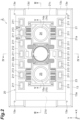
- the mirror device 20 includes a base 21, the movable mirror 22, and a drive unit 23.
- the base 21 includes a first surface 21a (surface on the one side in the Z-axis direction) and a second surface 21b opposite to the first surface 21a.
- Each of the first surface 21a and the second surface 21b is a main surface of the base 21.
- the base 21 has a rectangular plate shape, and a size of approximately 10 mm ⁇ 15 mm ⁇ 0.35 mm (thickness).
- the movable mirror 22 includes a mirror surface (optical function member) 22a, and a movable unit 22b in which the mirror surface 22a is disposed.
- the movable mirror 22 (movable unit 22b) is supported in the base 21 so that the movable mirror 22 can move in the Z-axis direction perpendicular to the first surface 21a (a predetermined direction perpendicular to the first surface).
- the drive unit 23 moves the movable mirror 22 in the Z-axis direction.
- a pair of light passage openings 24 and 25 are provided in the mirror device 20.
- the pair of light passage openings 24 and 25 are respectively disposed on both sides of the movable mirror 22 in the X-axis direction.
- the light passage opening (first light passage portion) 24 constitutes a first portion of an optical path between the beam splitter unit 3 and the fixed mirror 16.
- the light passage opening 25 does not function as a light passage opening.
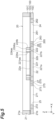
- FIG. 5 is a schematic cross-sectional view of the mirror device 20 illustrated in FIG. 3
- FIG. 5 schematically illustrates the mirror device 20, for example, in a state in which dimensions in the Z-axis direction are enlarged in comparison to actual dimensions.
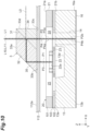
- the base 21, the movable unit 22b of the movable mirror 22, and the drive unit 23 are constituted by a silicon on insulator (SOI) substrate (semiconductor substrate) 100. That is, the mirror device 20 is constituted by the SOI substrate 100.
- the mirror device 20 is formed in a rectangular plate shape.
- the SOI substrate 100 includes a support layer 101, a device layer 102, and an intermediate layer 103.
- the support layer 101 is a first silicon layer (a first semiconductor layer).
- the device layer 102 is a second silicon layer (a second semiconductor layer).
- the intermediate layer 103 is an insulating layer that is disposed between the support layer 101 and the device layer 102.
- the SOI substrate 100 includes the support layer 101, the intermediate layer 103, and the device layer 102 in this order from the one side in the Z-axis direction.
- the base 21 is constituted by a part of the support layer 101, the device layer 102, and the intermediate layer 103.
- the first surface 21a of the base 21 is a surface of the support layer 101 which is opposite to the intermediate layer 103.
- the second surface 21b of the base 21 is a surface of the device layer 102 which is opposite to the intermediate layer 103.
- the support layer 101 that constitutes the base 21 is thicker than the device layer 102 that constitutes the base 21.
- the thickness of the support layer 101 that constitutes the base 21 is approximately four times the thickness of the device layer 102 that constitutes the base 21.
- the second surface 21b of the base 21 and a third surface 13a of the optical function member 13 are jointed to each other (refer to FIG. 3 and FIG. 4 ).
- the movable mirror 22 is disposed in a state in which an intersection between an axial line R1 and an axial line R2 is set as the central position (gravity center position).
- the axial line R1 is a straight line that extends in the X-axis direction.
- the axial line R2 is a straight line that extends in a Y-axis direction (a second direction perpendicular to the first direction and the third direction).
- a portion other than a portion that overlaps a sixth surface 21d of the base 21 to be described later has a shape that is linearly symmetric to each of the axial line R1 and the axial line R2.
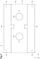
- the surface 14a of the light transmitting portion 14 and the surface 15a of the light transmitting portion 15 respectively face the light passage openings 24 and 25 of the mirror device 20. Accordingly, in the mirror unit 2, when the movable mirror 22 reciprocates in the Z-axis direction, the movable mirror 22 and the drive unit 23 are prevented from coming into contact with the optical function member 13.
- the remainder of the laser light L10 is transmitted through the first mirror surface 31, and reaches the mirror surface 16a of the fixed mirror 16 through the optical surface 33c, the light transmitting member 112, the light passage opening 24 of the mirror device 20, and the light transmitting portion 14 of the optical function member 13.
- the remainder of the laser light L10 is reflected by the mirror surface 16a of the fixed mirror 16, proceeds on the same optical path P4 in an opposite direction, and is transmitted through the first mirror surface 31.
- the part of the laser light L10 which is reflected by the first mirror surface 31, and the remainder of the laser light L10 which is transmitted through the first mirror surface 31 become interference light L11, and the interference light L11 of the laser light is emitted from the beam splitter unit 3 through the optical surface 33a along the Z-axis direction.
- the light passage opening 24 of the mirror device 20 constitutes a first portion P2a of the optical path P2 of the measurement light L0 and a first portion P4a of the optical path P4 of the laser light L10 in an optical path between the beam splitter unit 3 and the fixed mirror 16.
- the light transmitting portion 14 of the optical function member 13 constitutes a second portion P2b of the optical path P2 of the measurement light L0 and a second portion P4b of the optical path P4 of the laser light L10 in the optical path between the beam splitter unit 3 and the fixed mirror 16.
- the second portion P2b of the optical path P2 of the measurement light 1.0 is constituted by the light transmitting portion 14, thus an optical path difference between both the optical paths P1 and P2 is corrected so that a difference between an optical path length (optical path length in consideration of a refractive index of respective media through which the optical path passes) of the optical path P1 of the measurement light L0, and an optical path length of the optical path P2 of the measurement light L0 decreases.
- the second portion P4b of the optical path P4 of the laser light L10 is constituted by the light transmitting portion 14, thus an optical path difference between both the optical paths P3 and P4 is corrected so that a difference between an optical path length of the optical path P3 of the laser light L10 and an optical path length of the optical path P4 of the laser light L10 decreases.
- a refractive index of the light transmitting portion 14 is the same as a refractive index of the respective optical blocks which constitute the beam splitter unit 3, and a distance between the first mirror surface 31 and the second mirror surface 32 in the X-axis direction is the same as the thickness of the light transmitting portion 14 in the Z-axis direction (that is, a distance between the surface 14a of the light transmitting portion 14 and the fourth surface 13b of the optical function member 13 in the Z-axis direction).
- the second support structure 12 includes a connection unit 120.
- the connection unit 120 includes a main body portion 121, a frame body 122, and a fixing plate 123.
- the main body portion 121 includes a pair of side wall portions 124 and 125, and a ceiling wall portion 126.
- the pair of side wall portions 124 and 125 face each other in the X-axis direction.
- An opening 124a is formed in the side wall portion 124 on one side in the X-axis direction.
- the ceiling wall portion 126 faces the support 9 in the Z-axis direction.
- An opening 126a is formed in the ceiling wall portion 126.
- the main body portion 121 is integrally formed of a metal.
- a plurality of positioning pins 121a are provided in the main body portion 121.
- the main body portion 121 is positioned with respect to the support 9 by inserting the positioning pins 121a into the reference hole 9b and the hole 9c which are formed in the support 9, and is attached to the support 9 in this state, for example, by a bolt.
- the frame body 122 is disposed on a surface of the side wall portion 124 on a side opposite to the beam splitter unit 3. An opening of the frame body 122 faces the beam splitter unit 3 through the opening 124a of the side wall portion 124.
- the light incident unit 4 is disposed in the frame body 122.
- the fixing plate 123 is a member that fixes the light incident unit 4 disposed in the frame body 122 to the main body portion 121 (details will be described later).
- the second support structure 12 further includes a holding unit 130.
- the holding unit 130 includes a main body portion 131, a frame body 132 and a fixing plate 133.
- the main body portion 131 is attached to a surface of the ceiling wall portion 126 which is opposite to the support 9.
- the main body portion 131 is positioned with respect to the main body portion 121 of the connection unit 120 by a plurality of positioning pins 131a, and is attached to the ceiling wall portion 126 in this state, for example, by a bolt.
- a concave portion 134 is formed in a surface of the main body portion 131 which is opposite to the support 9.
- a first light passage hole 135, a second light passage hole 136, and a third light passage hole 137 are formed in a bottom surface of the concave portion 134.
- the first light passage hole 135 is formed at a position that faces the first mirror surface 31 of the beam splitter unit 3 in the Z-axis direction.
- the second light passage hole 136 is formed on the other side of the first light passage hole 135 in the X-axis direction (that is, on a side opposite to the light incident unit 4).
- the third light passage hole 137 is formed on the other side of the second light passage hole 136 in the X-axis direction.
- the frame body 132 is disposed on the bottom surface of the concave portion 134. An opening of the frame body 132 faces the third light passage hole 137.
- the second light source 7 is disposed in the frame body 132.
- the first light detector 6 is disposed on the bottom surface of the concave portion 134 in a state of facing the first light passage hole 135.
- the second light detector 8 is disposed on the bottom surface of the concave portion 134 in a state of facing the second light passage hole 136.
- the fixing plate 133 is a member that fixes the first light detector 6 and the second light detector 8 which are disposed on the bottom surface of the concave portion 134, and the second light source 7 that is disposed in the frame body 132 to the main body portion 131 (details will be described later).
- the light incident unit 4 includes a holder 41 and a collimator lens 42.
- the holder 41 holds the collimator lens 42, and is configured so that an optical fiber (not illustrated) that guides the measurement light L0 can be connected to the holder 41.
- the collimator lens 42 collimates the measurement light L0 emitted from the optical fiber.
- an optical axis of the optical fiber matches an optical axis of the collimator lens 42.
- a flange portion 41a is provided in the holder 41.
- the flange portion 41a is disposed between the frame body 122 and the fixing plate 123.
- fixing plate 123 is attached to the side wall portion 124, for example, by a bolt, and the light incident unit 4 disposed in the frame body 122 is fixed to the main body portion 121.
- the light incident unit 4 is disposed on one side of the beam splitter unit 3 in the X-axis direction, and is supported by the second support structure 12.
- the light incident unit 4 allows measurement light L0 that is incident from the first light source through a measurement target or measurement light L0 that is generated from the measurement target (in this embodiment, the measurement light L0 guided by the optical fiber) to be incident to the beam splitter unit 3.
- a filter 54 is attached to the frame body 122.
- the filter 54 has a function of cutting off the laser light L10.
- the filter 54 is disposed in the opening 124a of the side wall portion 124 in a state of being inclined with respect to an optical axis of the light incident unit 4.
- the filter 54 closes the opening of the frame body 122 when viewed form the X-axis direction.
- the filter 54 is disposed between the light incident unit 4 and the beam splitter unit 3, and is supported by the second support structure 12 in a state of being inclined with respect to an optical axis of the light incident unit 4.
- an optical surface of the filter 54 is a surface that is parallel to the Z-axis direction and has an angle of 10° to 20° with respect to the Y-axis direction.
- the optical axis of the light incident unit 4 is parallel to the X-axis direction.
- the filter 54 is inclined with respect to the optical axis of the light incident unit 4, light in the same wavelength range as the laser light L10 is reflected to the outside of an interference optical system, and thus it is possible to reliably prevent the light from being stray light.
- the first light detector 6 includes a holder 61, a light detection element 62, and a condensing lens 63.
- the holder 61 holds the light detection element 62 and the condensing lens 63.
- the light detection element 62 detects the interference light L1 of the measurement light.
- the light detection element 62 is an InGaAs photodiode.
- the condensing lens 63 condenses the interference light L1 of the measurement light incident to the light detection element 62 to the light detection element 62.
- an optical axis of the light detection element 62 and an optical axis of the condensing lens 63 match each other.
- a flange portion 61a is provided in the holder 61.
- the flange portion 61a is disposed between the bottom surface of the concave portion 134 of the main body portion 131, and the fixing plate 133.
- the fixing plate 133 is attached to the main body portion 131, for example, by a bolt, and thus the first light detector 6 disposed on the bottom surface of the concave portion 134 is fixed to the main body portion 131.
- the first light detector 6 is disposed on one side of the beam splitter unit 3 in the Z-axis direction, and is supported by the second support structure 12.
- the first light detector 6 faces the first mirror surface 31 of the beam splitter unit 3 in the Z-axis direction.
- the first light detector 6 detects the interference light L1 of the measurement light emitted from the beam splitter unit 3.
- the second light detector 8 includes a holder 81, a light detection element 82, and a condensing lens 83.
- the holder 81 holds the light detection element 82 and the condensing lens 83.
- the light detection element 82 detects the interference light L11 of the laser light.
- the light detection element 82 is a Si photodiode.
- the condensing lens 83 condenses the interference light L11 of the laser light incident to the light detection element 82 to the light detection element 82.
- an optical axis of the light detection element 82 and an optical axis of the condensing lens 83 match each other.
- a flange portion 81a is provided in the holder 81.
- the flange portion 81a is disposed between the bottom surface of the concave portion 134 of the main body portion 131, and the fixing plate 133.
- the fixing plate 133 is attached to the main body portion 131, for example, by a bolt, and thus the second light detector 8 disposed on the bottom surface of the concave portion 134 is fixed to the main body portion 131.
- the second light detector 8 is disposed on one side of the beam splitter unit 3 in the Z-axis direction, and is supported by the second support structure 12.
- the second light detector 8 detects the interference light L11 of the laser light emitted from the beam splitter unit 3.
- the second light source 7 includes a holder 71, a light-emitting element 72, and a collimator lens 73.
- the holder 71 holds the light-emitting element 72 and the collimator lens 73.
- the light-emitting element 72 emits the laser light L10.
- the light-emitting element 72 is a semiconductor laser such as a VCSEL.
- the collimator lens 73 collimates the laser light L10 emitted from the light-emitting element 72.
- an optical axis of the light-emitting element 72 and an optical axis of the collimator lens 73 match each other.
- a flange portion 71a is provided in the holder 71.
- the flange portion 71a is disposed between the frame body 132 and the fixing plate 133.
- the fixing plate 133 is attached to the main body portion 131, for example, by a bolt, and thus the second light source 7 disposed in the frame body 132 is fixed to the main body portion 131.
- the second light source 7 is disposed on one side of the beam splitter unit 3 in the Z-axis direction, and is supported by the second support structure 12.
- the second light source 7 emits the laser light L10 that is to be incident to the beam splitter unit 3.
- the holding unit 130 holds the first light detector 6, the second light detector 8, and the second light source 7 so that the first light detector 6, the second light detector 8, and the second light source 7 are aligned in this order from one side (that is, the light incident unit 4 side) in the X-axis direction.
- a first mirror 51, a second mirror 52, and a third mirror 53 are attached to the main body portion 131 of the holding unit 130.
- the first mirror 51 is held by the holding unit 130 to be located on a side opposite to the first light detector 6 with respect to the first light passage hole 135.
- the second mirror 52 is held by the holding unit 130 to be located on a side opposite to the second light detector 8 with respect to the second light passage hole 136.
- the third mirror 53 is held by the holding unit 130 to be located on a side opposite to the second light source 7 with respect to the third light passage hole 137.
- the second mirror 52 is a mirror (for example, a half mirror) that has a function of reflecting a part of the laser light L10 and allowing the remainder of the laser light L10 to be transmitted therethrough, and is parallel to the first mirror 51.
- the second mirror 52 is disposed to overlap the first mirror 51 when viewed from the X-axis direction, and to overlap the second light detector 8 when viewed from the Z-axis direction. That is, the second mirror 52 is disposed to face the first mirror 51 and the second light detector 8.
- an optical surface of the second mirror 52 is a surface that is parallel to the Y-axis direction, and has an angle of 45° with respect to the Z-axis direction.
- the third mirror 53 is a mirror (for example, a total reflection mirror) that has a function of reflecting the laser light L10 and is parallel to the second mirror 52.
- the third mirror 53 is disposed to overlap the second mirror 52 when viewed from the X-axis direction, and overlap the second light source 7 when viewed from the Z-axis direction. That is, the third mirror 53 is disposed to face the second mirror 52 and the second light source 7.
- an optical surface of the third mirror 53 is a surface that is parallel to the Y-axis direction, and has an angle of 45° with respect to the Z-axis direction.
- the interference light L1 of the measurement light which is emitted from the beam splitter unit 3 in the Z-axis direction, is transmitted through the first mirror 51, is incident to the first light detector 6 through the aperture 55, and is detected by the first light detector 6.
- the laser light L10 emitted from the second light source 7 is reflected by the third mirror 53, is transmitted through the second mirror 52, is reflected by the first mirror 51, and is incident to the beam splitter unit 3 in the Z-axis direction.
- the interference light L11 of the laser light which is emitted from the beam splitter unit 3 in the Z-axis direction, is reflected by the first mirror 51 and the second mirror 52, is incident to the second light detector 8, and is detected by the second light detector 8.
- the first surface 21a of the base 21 (a surface on one side in the Z-axis direction) is located more to the one side than the mirror surface 22a. Accordingly, it is possible to protect the mirror surface 22a by the base 21 and it is possible to prevent the mirror surface 22a from being damaged, for example, due to direct contact in transportation or the like.
- the support layer 101 that constitutes the base 21 is thicker than the device layer 102 that constitutes the base 21. Accordingly, it is possible to secure a protrusion amount of the base 21 with respect to the mirror surface 22a, and it is possible to effectively protect the mirror surface 22a by the base 21. Accordingly, according to the mirror device 20, it is possible to enhance reliability.
- a “configuration in which the first surface 21a of the base 21 is located more to the one side than the mirror surface 22a” represents that "at least a part of the first surface 21a is located more to the one side than the mirror surface 22a".
- the entirety of the first surface 21a is located more to the one side in the Z-axis direction than the mirror surface 22a.
- the entirety of the mirror surface 22a is located more tothe other side in the Z-axis direction than the first surface 21a.
- the "surface of the base on the one side in the Z-axis direction” is an "end surface of the base on the one side in the Z-axis direction” or a "surface located on the most one side in the Z-axis direction among surfaces of the base”.
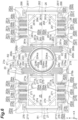
- End surfaces (end surfaces 224as, 224bs, and 224cs) of the rib portion 224 on one side in the Z-axis direction are located more to the one side than the mirror surface 22a. Accordingly, it is also possible to protect the mirror surface 22a by the rib portion 224. In addition, it is also possible to suppress deformation of the movable unit 22b during movement by the rib portion 224.
- the rib portion 224 includes the inner rib portion 224a that is disposed on a surface on one side in the arrangement portion 221 to extend along an outer edge of the arrangement portion 221 when viewed from the Z-axis direction. Accordingly, the inner rib portion 224a is disposed to be closer to the mirror surface 22a, and thus it is possible to more effectively protect the mirror surface 22a. In addition, the inner rib portion 224a is disposed on the arrangement portion 221, and thus it is possible to more appropriately suppress deformation of the arrangement portion 221.
- the rib portion 224 includes the outer rib portion 224b that is disposed on a surface on one side in the frame portion 222 to extend along the frame portion 222 when viewed from the Z-axis direction. Accordingly, it is possible to more effectively protect the mirror surface 22a due to the rib portion 224. In addition, it is possible to suppress deformation of the frame portion 222 due to the outer rib portion 224b, and it is possible to suppress deformation of the arrangement portion 221 which is caused by deformation of the frame portion 222.
- the groove 216 that reaches the device layer 102 from the surface 101a (surface on one side in the Z-axis direction) of the support layer 101 and extends to surround the opening 213 when viewed from the Z-axis direction is formed in the base 21. Accordingly, it is possible to reliably secure an electrical insulation property of the electrode pads 211 due to the groove 216, and it is possible to further enhance reliability.
- the mirror device 20 may include a hole or a notch that is formed in the base 21 as a first light passage portion instead of the light passage opening 24 or the light passage opening 25.
- the semiconductor substrate that constitutes the mirror device 20 may not be the SOI substrate, and may be a substrate including a first semiconductor layer, an insulating layer, and a second semiconductor layer in this order from one side in the Z-axis direction.
- Each of the inner rib portion 224a, the outer rib portion 224b, and the connection rib portion 224c may be formed in any shape.
- the rib portions may extend obliquely with respect to X-axis direction or the Y-axis direction, or may extend in a zigzag shape.
- the arrangement, the number, the length, the width, and the thickness of the rib portions may be arbitrarily set.
- the thicknesses of the inner rib portion 224a, the outer rib portion 224b, and the connection rib portion 224c may be different from each other. At least one of the rib portions may be omitted.
- 3 beam splitter unit, 13: optical function member, 14: light transmitting portion (second light passage portion), 16: fixed mirror, 20: mirror device (optical device), 21: base, 21a: first surface (main surface), 21b: second surface (main surface), 22a: mirror surface (optical function unit), 22b: movable unit, 221: arrangement portion, 222: frame portion, 223: connection portion, 224: rib portion, 24: light passage opening (first light passage portion), 100: SOI substrate (semiconductor substrate), 101: support layer (first semiconductor layer), 101a: surface, 102: device layer (second semiconductor layer), 102a: surface, 103: intermediate layer (insulating layer), 211: electrode pad, 213: opening, 214: bottom surface, 215: lateral surface, 216: groove.
Landscapes
- Physics & Mathematics (AREA)
- Spectroscopy & Molecular Physics (AREA)
- General Physics & Mathematics (AREA)
- Optics & Photonics (AREA)
- Engineering & Computer Science (AREA)
- Computer Hardware Design (AREA)
- Microelectronics & Electronic Packaging (AREA)
- Analytical Chemistry (AREA)
- Chemical & Material Sciences (AREA)
- Mechanical Engineering (AREA)
- Mechanical Light Control Or Optical Switches (AREA)
- Micromachines (AREA)
- Spectrometry And Color Measurement (AREA)
- Instruments For Measurement Of Length By Optical Means (AREA)
- Mounting And Adjusting Of Optical Elements (AREA)
- Optical Elements Other Than Lenses (AREA)
- Optical Couplings Of Light Guides (AREA)
- Led Device Packages (AREA)
- Glass Compositions (AREA)
Claims (9)
- Module (1) optique comprenant une partie (2) de miroir et une partie (3) de séparateur de faisceau ;
la partie (2) de miroir comprenant :
un dispositif (20) optique comprenant :une base (21) qui inclut une surface (21a, 21b) principale ;une partie (22b) mobile qui est supportée dans la base (21) pour se déplacer le long d'une direction (Z) prédéterminée qui croise la surface (21a, 21b) principale ;une partie (28) d'actionnement pour déplacer l'unité (22b) mobile le long de la direction (Z) prédéterminée ; etune partie (22a) fonctionnelle optique qui est disposée sur la partie (22b) mobile,dans lequel la base (21) et la partie (22b) mobile sont constituées d'un substrat semi-conducteur qui inclut une première couche (101) de semi-conducteur, une couche (103) isolante, et une seconde couche (102) de semi-conducteur dans cet ordre à partir d'un côté dans la direction (Z) prédéterminée,la base (21) est constituée par la première couche (101) de semi-conducteur, la couche (103) isolante, et la seconde couche (102) de semi-conducteur,la partie (22b) mobile inclut une partie de placement qui est constituée par la seconde couche (102) de semi-conducteur,la partie (22a) fonctionnelle optique est disposée sur une surface de la partie de placement sur ledit un côté,la première couche (101) de semi-conducteur qui constitue la base (21) est plus épaisse que la seconde couche (102) de semi-conducteur qui constitue la base (21), etune surface de la base (21) sur ledit un côté est située au-dessus de la partie (22a) fonctionnelle optique dans la direction (Z) prédéterminée ;la partie (2) de miroir comprenant en outre :un organe (13) fonctionnel optique qui est disposé de l'autre côté dans la direction (Z) prédéterminée par rapport au dispositif (20) optique, l'organe (13) fonctionnel optique étant transparent et présentant une forme de plaque ; etun miroir (16) fixe qui est disposé de l'autre côté, qui est le côté opposé au dispositif (20) optique, dans la direction de l'axe Z, par rapport à l'organe (13) fonctionnel optique ;dans lequel la partie (22a) fonctionnelle optique est une surface de miroir qui constitue un miroir mobile en combinaison avec la partie (22b) mobile ; etdans lequel la partie (3) de séparateur de faisceau constitue un système optique d'interférence en combinaison avec le miroir mobile et le miroir (16) fixe. - Module (1) optique selon la revendication 1,dans lequel la partie (22b) mobile inclut en outre une partie (224) de nervure qui est disposée à la périphérie de la partie fonctionnelle optique,la partie (224) de nervure est constituée par la première couche (101) de semi-conducteur et la couche isolante qui sont disposées sur la seconde couche (102) de semi-conducteur, etune surface d'extrémité de la partie (224) de nervure sur ledit un côté est située plus vers ledit un côté que la partie fonctionnelle optique.
- Module (1) optique selon la revendication 2,
dans lequel la partie (224) de nervure est disposée sur la surface de la partie de placement sur ledit un côté pour s'étendre le long d'un bord extérieur de la partie de placement lorsqu'elle est vue depuis la direction prédéterminée. - Module (1) optique selon la revendication 2 ou la revendication 3,dans lequel la partie (22b) mobile inclut en outre une partie (222) de cadre qui entoure la partie de placement lorsqu'elle est vue depuis la direction prédéterminée, et une partie (223) de connexion qui relie la partie de placement et la partie (222) de cadre,la partie (222) de cadre et la partie (223) de connexion sont constituées par la seconde couche (102) de semi-conducteur, etla partie (224) de nervure est disposée sur une surface de la partie (222) de cadre sur ledit un côté pour s'étendre le long de la partie (222) de cadre lorsqu'elle est vue à partir de la direction prédéterminée.
- Module (1) optique selon l'une quelconque des revendications 2 à 4,
dans lequel la première couche (101) de semi-conducteur qui constitue la partie (224) de nervure est plus mince que la première couche (101) de semi-conducteur qui constitue la base (21). - Module (1) optique selon l'une quelconque des revendications 1 à 5, comprenant en outre :un tampon (211) d'électrode qui est fourni à la base (21),dans lequel le tampon (211) d'électrode est disposé sur une surface de la seconde couche (102) de semi-conducteur sur ledit un côté dans une ouverture qui est formée dans une surface de la première couche (101) de semi-conducteur sur ledit un côté pour atteindre la seconde couche (102) de semi-conducteur, etla base (21) inclut une rainure (216) qui est formée dans la surface de la première couche (101) de semi-conducteur sur ledit un côté pour atteindre la seconde couche (102) de semi-conducteur, et s'étend pour entourer l'ouverture lorsqu'elle est vue depuis la direction prédéterminée.
- Module (1) optique selon la revendication 6,
dans lequel le tampon (211) d'électrode s'étend le long d'une surface inférieure et d'une surface latérale de l'ouverture. - Module (1) optique selon la revendication 6 ou la revendication 7,dans lequel chacune du tampon (211) d'électrode et de l'unité fonctionnelle optique est constituée d'une couche métallique, etla couche métallique qui constitue le tampon (211) d'électrode est plus épaisse que la couche métallique qui constitue l'unité fonctionnelle optique.
- Module (1) optique selon la revendication 1, dans lequel :le dispositif (20) optique est doté d'une première partie de passage de lumière qui constitue une première partie d'un chemin optique entre la partie (3) de séparateur de faisceau, et le miroir (16) fixe,l'organe (13) fonctionnel optique est doté d'une seconde partie de passage de lumière qui constitue une seconde partie du chemin optique entre la partie (3) de séparateur de faisceau et le miroir (16) fixe, etla seconde partie de passage de lumière corrige une différence de chemin optique qui se produit entre un chemin optique entre la partie (3) de séparateur de faisceau et le miroir mobile, et le chemin optique entre la partie (3) de séparateur de faisceau et le miroir (16) fixe.
Priority Applications (1)
| Application Number | Priority Date | Filing Date | Title |
|---|---|---|---|
| EP25163506.6A EP4546024A3 (fr) | 2017-07-06 | 2018-07-06 | Dispositif optique |
Applications Claiming Priority (2)
| Application Number | Priority Date | Filing Date | Title |
|---|---|---|---|
| JP2017133089 | 2017-07-06 | ||
| PCT/JP2018/025646 WO2019009403A1 (fr) | 2017-07-06 | 2018-07-06 | Dispositif optique |
Related Child Applications (1)
| Application Number | Title | Priority Date | Filing Date |
|---|---|---|---|
| EP25163506.6A Division EP4546024A3 (fr) | 2017-07-06 | 2018-07-06 | Dispositif optique |
Publications (3)
| Publication Number | Publication Date |
|---|---|
| EP3650908A1 EP3650908A1 (fr) | 2020-05-13 |
| EP3650908A4 EP3650908A4 (fr) | 2021-04-07 |
| EP3650908B1 true EP3650908B1 (fr) | 2025-04-02 |
Family
ID=64950093
Family Applications (9)
| Application Number | Title | Priority Date | Filing Date |
|---|---|---|---|
| EP18827624.0A Active EP3650908B1 (fr) | 2017-07-06 | 2018-07-06 | Dispositif optique |
| EP18828441.8A Active EP3650914B1 (fr) | 2017-07-06 | 2018-07-06 | Dispositif optique |
| EP18827369.2A Active EP3650907B1 (fr) | 2017-07-06 | 2018-07-06 | Unité de miroir et module optique |
| EP23209352.6A Pending EP4300058A3 (fr) | 2017-07-06 | 2018-07-06 | Module optique |
| EP25163506.6A Pending EP4546024A3 (fr) | 2017-07-06 | 2018-07-06 | Dispositif optique |
| EP18828564.7A Pending EP3650820A4 (fr) | 2017-07-06 | 2018-07-06 | Module optique |
| EP18828315.4A Active EP3650913B1 (fr) | 2017-07-06 | 2018-07-06 | Module optique |
| EP18827625.7A Active EP3650909B1 (fr) | 2017-07-06 | 2018-07-06 | Module optique |
| EP18828669.4A Active EP3650915B1 (fr) | 2017-07-06 | 2018-07-06 | Unité de miroirs et module optique |
Family Applications After (8)
| Application Number | Title | Priority Date | Filing Date |
|---|---|---|---|
| EP18828441.8A Active EP3650914B1 (fr) | 2017-07-06 | 2018-07-06 | Dispositif optique |
| EP18827369.2A Active EP3650907B1 (fr) | 2017-07-06 | 2018-07-06 | Unité de miroir et module optique |
| EP23209352.6A Pending EP4300058A3 (fr) | 2017-07-06 | 2018-07-06 | Module optique |
| EP25163506.6A Pending EP4546024A3 (fr) | 2017-07-06 | 2018-07-06 | Dispositif optique |
| EP18828564.7A Pending EP3650820A4 (fr) | 2017-07-06 | 2018-07-06 | Module optique |
| EP18828315.4A Active EP3650913B1 (fr) | 2017-07-06 | 2018-07-06 | Module optique |
| EP18827625.7A Active EP3650909B1 (fr) | 2017-07-06 | 2018-07-06 | Module optique |
| EP18828669.4A Active EP3650915B1 (fr) | 2017-07-06 | 2018-07-06 | Unité de miroirs et module optique |
Country Status (6)
| Country | Link |
|---|---|
| US (12) | US11187579B2 (fr) |
| EP (9) | EP3650908B1 (fr) |
| JP (15) | JP6496463B1 (fr) |
| CN (14) | CN113376827B (fr) |
| TW (2) | TWI853377B (fr) |
| WO (7) | WO2019009400A1 (fr) |
Families Citing this family (16)
| Publication number | Priority date | Publication date | Assignee | Title |
|---|---|---|---|---|
| US11513339B2 (en) | 2017-03-14 | 2022-11-29 | Hamamatsu Photonics K.K. | Optical module |
| JP6778134B2 (ja) * | 2017-03-14 | 2020-10-28 | 浜松ホトニクス株式会社 | 光モジュール及びその実装方法 |
| CN110392858B (zh) | 2017-03-14 | 2021-08-13 | 浜松光子学株式会社 | 光模块 |
| EP3650908B1 (fr) | 2017-07-06 | 2025-04-02 | Hamamatsu Photonics K.K. | Dispositif optique |
| US11333882B2 (en) | 2019-01-30 | 2022-05-17 | Hamamatsu Photonics K.K. | Optical unit |
| JP6688917B1 (ja) * | 2019-01-30 | 2020-04-28 | 浜松ホトニクス株式会社 | 光モジュール、信号処理システム及び信号処理方法 |
| EP3865453A1 (fr) * | 2020-02-13 | 2021-08-18 | Miraex SA | Capteur de système micro-opto-mécanique, agencement et procédé de fabrication |
| US11360294B2 (en) | 2020-05-15 | 2022-06-14 | Samsung Electronics Co., Ltd. | Optical sensor |
| DE102021203930A1 (de) * | 2021-04-20 | 2022-10-20 | Continental Automotive Technologies GmbH | Spiegel für ein Head-Up-Display |
| JP2024017359A (ja) | 2022-07-27 | 2024-02-08 | セイコーエプソン株式会社 | 光学デバイスおよび分光装置 |
| JP2024022043A (ja) | 2022-08-05 | 2024-02-16 | セイコーエプソン株式会社 | 光学デバイスおよび分光装置 |
| JP2024121186A (ja) | 2023-02-27 | 2024-09-06 | セイコーエプソン株式会社 | 光学デバイスおよび分光装置 |
| JP2024134720A (ja) | 2023-03-22 | 2024-10-04 | セイコーエプソン株式会社 | 光学デバイス、分光装置および分光方法 |
| JP2024134721A (ja) * | 2023-03-22 | 2024-10-04 | セイコーエプソン株式会社 | 分光装置および形状測定装置 |
| JP2024168496A (ja) | 2023-05-24 | 2024-12-05 | セイコーエプソン株式会社 | 干渉計 |
| CN117471633B (zh) * | 2023-10-17 | 2025-09-30 | 中国科学院合肥物质科学研究院 | 一种红外激光光学镜的调节机构 |
Citations (2)
| Publication number | Priority date | Publication date | Assignee | Title |
|---|---|---|---|---|
| DE102008019600A1 (de) * | 2008-04-18 | 2009-10-22 | Fraunhofer-Gesellschaft zur Förderung der angewandten Forschung e.V. | Optische Vorrichtung in gestapelter Bauweise und Verfahren zur Herstellung derselben |
| JP2011080854A (ja) * | 2009-10-07 | 2011-04-21 | Konica Minolta Holdings Inc | フーリエ変換分光器 |
Family Cites Families (160)
| Publication number | Priority date | Publication date | Assignee | Title |
|---|---|---|---|---|
| JPS60263801A (ja) | 1984-06-13 | 1985-12-27 | Toshiba Corp | レ−ザ干渉測長器 |
| GB2163548B (en) | 1984-08-09 | 1987-11-25 | Perkin Elmer Ltd | Interferometric apparatus particularly for use in ft spectrophotometer |
| US4962997A (en) * | 1988-04-21 | 1990-10-16 | Hewlett-Packard Company | Three color separation using subtractive dichroic beamsplitters |
| US4999498A (en) | 1989-06-05 | 1991-03-12 | Mobay Corporation | Remote sensing gas analyzer |
| DE4024299A1 (de) * | 1990-07-31 | 1992-02-06 | Fraunhofer Ges Forschung | Vorrichtung zum fokussieren eines lichtstrahles in wenigstens zwei fokuspunkten |
| GB9027480D0 (en) | 1990-12-19 | 1991-02-06 | Philips Electronic Associated | Interferometer |
| JP2979701B2 (ja) * | 1991-04-23 | 1999-11-15 | 株式会社ニコン | 干渉計 |
| JPH05172738A (ja) | 1991-12-24 | 1993-07-09 | Jasco Corp | 音響セル |
| US5585922A (en) | 1992-12-24 | 1996-12-17 | Nikon Corporation | Dual interferometer apparatus compensating for environmental turbulence or fluctuation and for quantization error |
| JPH07190712A (ja) | 1993-12-27 | 1995-07-28 | Nikon Corp | 干渉計 |
| JPH10253912A (ja) | 1997-01-13 | 1998-09-25 | Denso Corp | 光走査装置 |
| JP3405108B2 (ja) | 1997-01-24 | 2003-05-12 | 株式会社村田製作所 | 外力計測装置およびその製造方法 |
| JPH10281719A (ja) | 1997-04-08 | 1998-10-23 | Omron Corp | 境界線検出方法 |
| US5870221A (en) | 1997-07-25 | 1999-02-09 | Lucent Technologies, Inc. | Micromechanical modulator having enhanced performance |
| JPH11183116A (ja) * | 1997-12-18 | 1999-07-09 | Nikon Corp | 光波干渉測定方法および装置 |
| DE19815241A1 (de) | 1998-04-04 | 1999-10-07 | Heidenhain Gmbh Dr Johannes | Positionsmeßeinrichtung |
| JP3518376B2 (ja) | 1998-11-26 | 2004-04-12 | 安藤電気株式会社 | 光干渉計 |
| US6356689B1 (en) | 2000-03-25 | 2002-03-12 | Lucent Technologies, Inc. | Article comprising an optical cavity |
| US6411427B1 (en) * | 2000-09-28 | 2002-06-25 | Xerox Corporation | Structure for an optical switch on a glass substrate |
| US6392807B1 (en) * | 2000-12-22 | 2002-05-21 | Avanex Corporation | Tunable chromatic dispersion compensator utilizing a virtually imaged phased array and folded light paths |
| US20020135850A1 (en) | 2001-03-15 | 2002-09-26 | Hagelin Paul M. | Multistage rotatable actuator |
| GB2375184A (en) | 2001-05-02 | 2002-11-06 | Marconi Caswell Ltd | Wavelength selectable optical filter |
| US7593029B2 (en) * | 2001-08-20 | 2009-09-22 | Ricoh Company, Ltd. | Optical scanning device and image forming apparatus using the same |
| IL149016A0 (en) | 2002-04-07 | 2004-03-28 | Green Vision Systems Ltd Green | Method and device for real time high speed high resolution spectral imaging |
| JP4465949B2 (ja) * | 2002-07-16 | 2010-05-26 | セイコーエプソン株式会社 | ダイシング方法 |
| KR100451409B1 (ko) | 2002-10-15 | 2004-10-06 | 한국전자통신연구원 | 마이크로 광스위치 및 그 제조방법 |
| JP4007180B2 (ja) * | 2002-12-16 | 2007-11-14 | 株式会社デンソー | 光スイッチ及びその製造方法 |
| JP4352373B2 (ja) | 2003-01-28 | 2009-10-28 | 横河電機株式会社 | ファブリペローフィルタ |
| JP2004255487A (ja) | 2003-02-25 | 2004-09-16 | Nippon Telegr & Teleph Corp <Ntt> | Memsの製造方法 |
| JP2005024722A (ja) * | 2003-06-30 | 2005-01-27 | Ricoh Co Ltd | 振動ミラー、光走査装置および画像形成装置 |
| JP2005055670A (ja) * | 2003-08-04 | 2005-03-03 | Seiko Epson Corp | Memsデバイス及びその製造方法並びにmemsモジュール |
| KR20050043423A (ko) | 2003-11-06 | 2005-05-11 | 삼성전자주식회사 | 주파수 변조 가능한 공진형 스캐너 |
| WO2005089098A2 (fr) * | 2004-01-14 | 2005-09-29 | The Regents Of The University Of California | Miroir a bande ultra large mettant en oeuvre un reseau de sous-longueurs d'onde |
| JP2005223111A (ja) | 2004-02-05 | 2005-08-18 | Yokogawa Electric Corp | 波長可変レーザー |
| JP4314390B2 (ja) * | 2004-04-02 | 2009-08-12 | 京都電子工業株式会社 | 液体の絶対屈折率測定装置 |
| JP2005309099A (ja) | 2004-04-21 | 2005-11-04 | Seiko Epson Corp | 波長可変フィルタ及びその製造方法 |
| TWI235735B (en) | 2004-06-18 | 2005-07-11 | Walsin Lihwa Corp | Two-axis element and manufacturing method thereof |
| JP2006032716A (ja) | 2004-07-16 | 2006-02-02 | Topcon Corp | メンブレンチップ製造方法 |
| KR20060010421A (ko) * | 2004-07-28 | 2006-02-02 | 삼성전자주식회사 | 구동각도 향상을 위한 공간형 이중 콤전극 구조 및 이를이용한 마이크로 스캐너 |
| US20060238768A1 (en) * | 2005-04-26 | 2006-10-26 | Mks Instruments, Inc. | Fourier transform infrared spectrometer |
| JP4098792B2 (ja) | 2005-06-08 | 2008-06-11 | アンリツ株式会社 | ミラー装置 |
| JP4548245B2 (ja) | 2005-06-27 | 2010-09-22 | セイコーエプソン株式会社 | 波長可変フィルタ |
| JP2007021044A (ja) | 2005-07-20 | 2007-02-01 | Topcon Corp | 可変形状ミラーの変形方法、光学装置及び眼底観察装置 |
| JP2007042786A (ja) | 2005-08-02 | 2007-02-15 | Sony Corp | マイクロデバイス及びそのパッケージング方法 |
| JP2007114230A (ja) * | 2005-10-17 | 2007-05-10 | Japan Aviation Electronics Industry Ltd | 光スイッチ |
| US7453624B2 (en) | 2005-10-28 | 2008-11-18 | Miradia Inc. | Projection display system including a high fill ratio silicon spatial light modulator |
| US20070109552A1 (en) * | 2005-11-03 | 2007-05-17 | Felix Greg C | Optical interferometer |
| CN100362387C (zh) | 2005-11-18 | 2008-01-16 | 重庆大学 | 静电简支梁式干涉光调制器 |
| CN101316789B (zh) | 2005-11-25 | 2012-07-18 | 弗兰霍菲尔运输应用研究公司 | 可偏转微机械元件 |
| JP4473209B2 (ja) | 2005-12-02 | 2010-06-02 | アンリツ株式会社 | 可変波長光フィルタ |
| CN1815192A (zh) | 2006-03-14 | 2006-08-09 | 王辉 | 珠宝内部结构检测方法及其装置 |
| DE102006032667A1 (de) | 2006-07-13 | 2008-01-17 | Tesa Ag | Bahnförmiges Material mit einer Beschichtung, die ein sehr schnelles Spreiten beziehungsweise einen sehr schnellen Transport von Flüssigkeiten ermöglicht |
| US20080024767A1 (en) | 2006-07-28 | 2008-01-31 | Peter Seitz | Imaging optical coherence tomography with dynamic coherent focus |
| JP5098319B2 (ja) | 2006-12-12 | 2012-12-12 | コニカミノルタホールディングス株式会社 | 光スキャナ装置 |
| DE102006058563B3 (de) | 2006-12-12 | 2008-06-19 | Fraunhofer-Gesellschaft zur Förderung der angewandten Forschung e.V. | Mikrospiegel-Aktuator mit Kapselungsmöglichkeit sowie Verfahren zur Herstellung |
| US7630081B2 (en) | 2007-01-12 | 2009-12-08 | Sas Photonics, Llc | Interferometer maintaining optical relationship between elements |
| EP2111678B1 (fr) * | 2007-02-02 | 2015-04-08 | Finisar Corporation | Emballage stabilisant la temperature pour composants optoelectroniques dans un module d'emetteur |
| ES2525113T3 (es) | 2007-02-21 | 2014-12-18 | Agfa Healthcare N.V. | Sistema para tomografía de coherencia óptica |
| JP2008233405A (ja) | 2007-03-19 | 2008-10-02 | Yamagata Prefecture | 可変曲率ミラーデバイス及びその製造方法 |
| JP2009003429A (ja) * | 2007-05-18 | 2009-01-08 | Panasonic Corp | アクチュエータ |
| JP2008295174A (ja) | 2007-05-23 | 2008-12-04 | Panasonic Electric Works Co Ltd | 揺動装置、同装置を用いた光走査装置、映像表示装置、及び揺動装置の制御方法 |
| GB0713982D0 (en) | 2007-07-18 | 2007-08-29 | Univ Birmingham | Improved interferometer |
| US7690254B2 (en) | 2007-07-26 | 2010-04-06 | Honeywell International Inc. | Sensor with position-independent drive electrodes in multi-layer silicon on insulator substrate |
| JP2009042456A (ja) * | 2007-08-08 | 2009-02-26 | Toshiba Corp | 形状可変鏡装置およびこの形状可変鏡装置を用いた眼底観察装置 |
| US8174698B2 (en) | 2007-08-10 | 2012-05-08 | Corporation de l'Ecole Polytechnique de Montréal | MEMS tunable silicon fabry-perot cavity and applications thereof |
| JP2009093105A (ja) | 2007-10-12 | 2009-04-30 | Hoya Corp | マイクロミラー装置、およびミラー部形成方法 |
| JP5252687B2 (ja) | 2008-01-18 | 2013-07-31 | スタンレー電気株式会社 | 光偏向器 |
| GB0802290D0 (en) | 2008-02-08 | 2008-03-12 | Univ Kent Canterbury | Camera adapter based optical imaging apparatus |
| CN101285771B (zh) | 2008-06-04 | 2010-08-04 | 中国科学院长春光学精密机械与物理研究所 | 一种微型傅里叶变换光谱仪的制作方法 |
| CL2008002288A1 (es) | 2008-08-01 | 2010-06-11 | Univ Chile | Estructura nucleotidica que comprende al menos un casete de seleccion y/o expresion con un promotor, un terminador y un gen reportero de seleccion o expresion, flanqueado por un fragmento que permite su insercion; metodo de transformacion de organismos que genera organismos homocigotos, que emplea dicha estructura nucleotidica |
| KR101279441B1 (ko) | 2008-08-21 | 2013-07-05 | 삼성전자주식회사 | 멤스 미러, 미러 스캐너, 광주사 유닛 및 광주사 유닛을 채용한 화상형성장치 |
| JP5146204B2 (ja) | 2008-08-29 | 2013-02-20 | セイコーエプソン株式会社 | 光学デバイス、光スキャナ及び画像形成装置 |
| JP5098059B2 (ja) * | 2008-10-16 | 2012-12-12 | 国立大学法人東北大学 | ミラー装置及びミラー装置の製造方法 |
| RU2011122642A (ru) | 2008-11-04 | 2012-12-20 | Уилльям Марш Райз Юниверсити | Спектрометры с функцией картирования изображений |
| US8120781B2 (en) | 2008-11-26 | 2012-02-21 | Zygo Corporation | Interferometric systems and methods featuring spectral analysis of unevenly sampled data |
| JP5168659B2 (ja) | 2008-11-27 | 2013-03-21 | 株式会社リコー | 可動板構造体及び光走査装置 |
| US9285579B2 (en) | 2008-11-28 | 2016-03-15 | Hamamatsu Photonics K.K. | Light modulating device and laser processing device |
| JP5302020B2 (ja) | 2009-01-26 | 2013-10-02 | 浜松ホトニクス株式会社 | 光モジュール |
| JP5444746B2 (ja) | 2009-02-13 | 2014-03-19 | 富士通株式会社 | マイクロ可動素子および光干渉計 |
| US8736843B2 (en) | 2009-04-17 | 2014-05-27 | Si-Ware Systems | Opto-mechanical optical path retardation multiplier for optical MEMS applications |
| WO2010122879A1 (fr) | 2009-04-23 | 2010-10-28 | コニカミノルタホールディングス株式会社 | Mécanisme de réflexion de lumière, interféromètre optique et analyseur spectral |
| JP5316203B2 (ja) | 2009-04-24 | 2013-10-16 | ミツミ電機株式会社 | 圧電アクチュエータ及びその製造方法 |
| JP5590036B2 (ja) | 2009-09-28 | 2014-09-17 | コニカミノルタ株式会社 | 干渉光学系およびそれを備えた分光器 |
| WO2011037547A2 (fr) | 2009-09-28 | 2011-03-31 | Adam Bouras | Conversion de l'énergie des vagues |
| DE102009045720A1 (de) | 2009-10-15 | 2011-04-21 | Robert Bosch Gmbh | Mikromechanisches Bauteil mit einer verstellbaren Komponente |
| US8711361B2 (en) | 2009-11-05 | 2014-04-29 | Qualcomm, Incorporated | Methods and devices for detecting and measuring environmental conditions in high performance device packages |
| GB0920520D0 (en) | 2009-11-23 | 2010-01-06 | Univ Birmingham | Innovative laser interferometric angular read-out device |
| TWI416168B (zh) | 2010-02-05 | 2013-11-21 | Ind Tech Res Inst | 光學多環掃描元件 |
| JP2011170137A (ja) * | 2010-02-19 | 2011-09-01 | Seiko Epson Corp | 波長可変干渉フィルター、光センサーおよび分析機器 |
| US8873125B2 (en) | 2010-03-09 | 2014-10-28 | Si-Ware Systems | Technique to determine mirror position in optical interferometers |
| US9658107B2 (en) * | 2010-03-09 | 2017-05-23 | Si-Ware Systems | Self calibration for mirror positioning in optical MEMS interferometers |
| CN101871816B (zh) | 2010-06-03 | 2012-02-29 | 北京航空航天大学 | 模块化分体式Sagnac干涉仪 |
| JP2012026935A (ja) | 2010-07-26 | 2012-02-09 | Panasonic Electric Works Co Ltd | センサ装置 |
| JP5640549B2 (ja) | 2010-08-19 | 2014-12-17 | セイコーエプソン株式会社 | 光フィルター、光フィルターの製造方法および光機器 |
| US8582115B2 (en) | 2010-10-07 | 2013-11-12 | Omnivision Technologies, Inc. | Tunable and switchable multilayer optical devices |
| US8636911B2 (en) | 2010-10-07 | 2014-01-28 | Magic Technologies, Inc. | Process for MEMS scanning mirror with mass remove from mirror backside |
| JPWO2012056776A1 (ja) * | 2010-10-25 | 2014-03-20 | コニカミノルタ株式会社 | 分光器におけるチルト補正方法 |
| JP5640659B2 (ja) | 2010-11-02 | 2014-12-17 | セイコーエプソン株式会社 | 光フィルター、光フィルターの製造方法、及び光機器 |
| JP2012107962A (ja) * | 2010-11-16 | 2012-06-07 | Konica Minolta Holdings Inc | 干渉計およびそれを備えた分光器 |
| US8941062B2 (en) | 2010-11-16 | 2015-01-27 | 1087 Systems, Inc. | System for identifying and sorting living cells |
| JP5252235B2 (ja) * | 2010-11-26 | 2013-07-31 | ミツミ電機株式会社 | カメラモジュール |
| JP2012145675A (ja) | 2011-01-11 | 2012-08-02 | Seiko Epson Corp | 光フィルター、光フィルターの製造方法および光機器 |
| JP5703813B2 (ja) * | 2011-02-16 | 2015-04-22 | セイコーエプソン株式会社 | 波長可変干渉フィルター、光モジュール、及び光分析装置 |
| JP5817175B2 (ja) * | 2011-03-29 | 2015-11-18 | ソニー株式会社 | レンズモジュール、撮像装置、および電子機器 |
| CN202793315U (zh) | 2011-03-30 | 2013-03-13 | 迈普尔平版印刷Ip有限公司 | 差分干涉仪模块和具有差分干涉仪模块的光刻系统 |
| US9442014B2 (en) | 2011-04-05 | 2016-09-13 | Konica Minolta, Inc. | Fourier transform spectrometer and fourier transform spectroscopic method |
| US20140078509A1 (en) | 2011-05-02 | 2014-03-20 | Green Vision Systems Ltd. | Microelectromechanical system (mems) and (mem) optical interferometer for hyper-spectral imaging and analysis |
| JP5739224B2 (ja) * | 2011-05-16 | 2015-06-24 | 浜松ホトニクス株式会社 | 光学部品の製造方法及び光学部品 |
| JP5715481B2 (ja) | 2011-05-16 | 2015-05-07 | 浜松ホトニクス株式会社 | 光モジュール及びその製造方法 |
| WO2012164810A1 (fr) * | 2011-05-31 | 2012-12-06 | コニカミノルタオプティクス株式会社 | Spectromètre à transformée de fourier et procédé de spectroscopie à transformée de fourier |
| US9261405B2 (en) | 2011-07-13 | 2016-02-16 | Konica Minolta, Inc. | Interferometer and spectrometer including same |
| JP2013145356A (ja) * | 2011-12-13 | 2013-07-25 | Sumitomo Electric Ind Ltd | 光通信モジュール |
| JP5888002B2 (ja) | 2012-02-28 | 2016-03-16 | セイコーエプソン株式会社 | 波長可変干渉フィルター、光学フィルターデバイス、光学モジュール、及び電子機器 |
| CN103288034A (zh) | 2012-03-01 | 2013-09-11 | 北京大学 | 一种离面静电驱动器及其制作方法 |
| US8884725B2 (en) | 2012-04-19 | 2014-11-11 | Qualcomm Mems Technologies, Inc. | In-plane resonator structures for evanescent-mode electromagnetic-wave cavity resonators |
| US8994938B2 (en) | 2012-06-01 | 2015-03-31 | Thermo Scientific Portable Analytical Instruments Inc. | Raman spectroscopy using diffractive MEMS |
| CN102759402B (zh) | 2012-07-23 | 2014-11-26 | 北京理工大学 | 一种旋转式傅里叶变换干涉成像光谱仪 |
| JP6244616B2 (ja) * | 2012-08-30 | 2017-12-13 | セイコーエプソン株式会社 | 波長可変干渉フィルター、光学モジュール、電子機器、および波長可変干渉フィルターの製造方法 |
| JP5714648B2 (ja) * | 2012-11-16 | 2015-05-07 | 株式会社豊田中央研究所 | 力学量memsセンサ及び力学量memsセンサシステム |
| CN103885177B (zh) | 2012-12-21 | 2017-09-12 | 上海矽睿科技有限公司 | 光纤放大器动态增益斜率均衡器及其制备工艺 |
| US8922787B2 (en) | 2013-01-07 | 2014-12-30 | Si-Ware Systems | Spatial splitting-based optical MEMS interferometers |
| JP6036303B2 (ja) | 2013-01-07 | 2016-11-30 | セイコーエプソン株式会社 | パッケージ、光学モジュール、及び電子機器 |
| CN103076090B (zh) | 2013-01-22 | 2014-09-10 | 李剑平 | 一种激光干涉仪光程差定位方法及系统 |
| WO2014117158A1 (fr) | 2013-01-28 | 2014-07-31 | Si-Ware Systems | Auto-étalonnage destiné au positionnement d'un miroir dans des interféromètres optiques mems |
| DE102013203035A1 (de) * | 2013-02-25 | 2014-08-28 | Carl Zeiss Smt Gmbh | Optisches modul |
| JP6119325B2 (ja) | 2013-03-14 | 2017-04-26 | セイコーエプソン株式会社 | 干渉フィルター、干渉フィルターの製造方法、光学モジュール、電子機器、及び接合基板 |
| JP6015564B2 (ja) * | 2013-05-31 | 2016-10-26 | 株式会社デンソー | 光走査装置 |
| JP6285659B2 (ja) | 2013-08-05 | 2018-02-28 | 浜松ホトニクス株式会社 | 波長可変光源 |
| WO2015025691A1 (fr) | 2013-08-19 | 2015-02-26 | 浜松ホトニクス株式会社 | Procédé de fabrication d'un interféromètre optique |
| JP6467347B2 (ja) * | 2013-11-07 | 2019-02-13 | 住友精密工業株式会社 | 半導体装置 |
| EP4614224A3 (fr) * | 2013-12-23 | 2025-11-26 | Lg Innotek Co. Ltd | Appareil de déplacement de lentille |
| JP6347113B2 (ja) * | 2014-02-10 | 2018-06-27 | セイコーエプソン株式会社 | アクチュエーター、光スキャナー、画像表示装置およびヘッドマウントディスプレイ |
| CN103913235B (zh) | 2014-03-10 | 2016-07-06 | 中国科学院长春光学精密机械与物理研究所 | 基于moems技术的空间调制傅里叶变换红外光谱仪 |
| JP2015184592A (ja) | 2014-03-25 | 2015-10-22 | スタンレー電気株式会社 | 光偏向器 |
| KR20150130155A (ko) | 2014-05-13 | 2015-11-23 | 삼성전기주식회사 | 멤스 구조체 및 멤스 구조체의 제조 방법 |
| JP6115519B2 (ja) * | 2014-05-27 | 2017-04-19 | セイコーエプソン株式会社 | Mems駆動装置、電子機器、及びmems駆動方法 |
| CN104034422B (zh) | 2014-06-23 | 2016-04-13 | 中国科学院光电研究院 | 高稳定性转镜干涉仪 |
| CN104048759B (zh) | 2014-06-23 | 2016-04-13 | 中国科学院光电研究院 | 高稳定性转镜干涉仪 |
| JP6479354B2 (ja) | 2014-06-30 | 2019-03-06 | 浜松ホトニクス株式会社 | ミラー駆動装置及びその製造方法 |
| US9510110B2 (en) | 2014-07-07 | 2016-11-29 | Apple Inc. | Open top back plate optical microphone |
| JP2016085442A (ja) * | 2014-10-24 | 2016-05-19 | 株式会社リコー | 光偏向素子、光偏向器、2次元画像表示装置、光走査装置及び画像形成装置 |
| JP2016090250A (ja) | 2014-10-30 | 2016-05-23 | セイコーエプソン株式会社 | 分光測定装置及び保管ケース |
| WO2016080317A1 (fr) | 2014-11-20 | 2016-05-26 | 住友精密工業株式会社 | Élément optique |
| CN105890758B (zh) * | 2014-12-31 | 2018-06-15 | 南开大学 | 一种同时采用mems平动与扭转微镜的微型傅里叶红外光谱仪 |
| JP5962797B2 (ja) | 2015-02-26 | 2016-08-03 | セイコーエプソン株式会社 | 波長可変干渉フィルター、光モジュール、及び光分析装置 |
| JP3200481U (ja) * | 2015-02-26 | 2015-10-22 | 株式会社Est | レンズ駆動装置 |
| WO2016166872A1 (fr) | 2015-04-16 | 2016-10-20 | 株式会社島津製作所 | Spectrophotomètre à transformée de fourier |
| US9972971B2 (en) | 2015-07-13 | 2018-05-15 | Canon Kabushiki Kaisha | Surface emitting laser, information acquisition apparatus, and imaging apparatus |
| US9857223B2 (en) | 2015-11-20 | 2018-01-02 | Raytheon Company | Proximity focus imaging interferometer |
| JP6384676B2 (ja) | 2015-11-27 | 2018-09-05 | 京セラドキュメントソリューションズ株式会社 | 光偏向器及び該光偏向器を備えた画像形成装置 |
| CN205262613U (zh) | 2015-12-18 | 2016-05-25 | 南京信息工程大学 | 一种基于迈克尔逊干涉仪的连续激光波长测量实验仪 |
| JP6628622B2 (ja) | 2016-02-02 | 2020-01-15 | 浜松ホトニクス株式会社 | 光モジュール |
| TWI638419B (zh) | 2016-04-18 | 2018-10-11 | 村田製作所股份有限公司 | 一種掃描鏡設備與其製造方法 |
| CN105785549B (zh) * | 2016-05-19 | 2018-04-17 | 深圳市世尊科技有限公司 | 用于摄像模组的自动对焦音圈马达 |
| WO2017218778A1 (fr) | 2016-06-15 | 2017-12-21 | Si-Ware Systems | Unité spectrale intégrée |
| JP6880625B2 (ja) * | 2016-09-29 | 2021-06-02 | セイコーエプソン株式会社 | 光スキャナー、画像表示装置、ヘッドマウントディスプレイおよびヘッドアップディスプレイ |
| CN106500591B (zh) | 2016-12-26 | 2018-12-11 | 哈尔滨工程大学 | 一种集成式多波段迈克尔逊干涉仪 |
| GB2560494B (en) * | 2017-02-15 | 2021-11-10 | Gooch & Housego Torquay Ltd | Improvements in or relating to optical devices |
| EP3650908B1 (fr) * | 2017-07-06 | 2025-04-02 | Hamamatsu Photonics K.K. | Dispositif optique |
| US11668925B2 (en) | 2020-03-25 | 2023-06-06 | Compertum Microsystems Inc. | MEMS micro-mirror device with stopper and method of making same |
-
2018
- 2018-07-06 EP EP18827624.0A patent/EP3650908B1/fr active Active
- 2018-07-06 JP JP2019503582A patent/JP6496463B1/ja active Active
- 2018-07-06 TW TW111148790A patent/TWI853377B/zh active
- 2018-07-06 JP JP2018554595A patent/JP6461446B1/ja active Active
- 2018-07-06 EP EP18828441.8A patent/EP3650914B1/fr active Active
- 2018-07-06 WO PCT/JP2018/025642 patent/WO2019009400A1/fr not_active Ceased
- 2018-07-06 EP EP18827369.2A patent/EP3650907B1/fr active Active
- 2018-07-06 CN CN202110691193.XA patent/CN113376827B/zh active Active
- 2018-07-06 CN CN202210118147.5A patent/CN114509856A/zh active Pending
- 2018-07-06 EP EP23209352.6A patent/EP4300058A3/fr active Pending
- 2018-07-06 CN CN201880043077.3A patent/CN110799885B/zh active Active
- 2018-07-06 CN CN201880040988.0A patent/CN110770625B/zh active Active
- 2018-07-06 US US16/619,630 patent/US11187579B2/en active Active
- 2018-07-06 CN CN202210538583.8A patent/CN114755817B/zh active Active
- 2018-07-06 US US16/625,682 patent/US11054309B2/en active Active
- 2018-07-06 WO PCT/JP2018/025641 patent/WO2019009399A1/fr not_active Ceased
- 2018-07-06 US US16/625,693 patent/US11629947B2/en active Active
- 2018-07-06 CN CN201880040989.5A patent/CN110799881B/zh active Active
- 2018-07-06 WO PCT/JP2018/025648 patent/WO2019009404A1/fr not_active Ceased
- 2018-07-06 CN CN201880037794.5A patent/CN110720069B/zh active Active
- 2018-07-06 JP JP2019503580A patent/JP6514841B1/ja active Active
- 2018-07-06 WO PCT/JP2018/025645 patent/WO2019009402A1/fr not_active Ceased
- 2018-07-06 US US16/625,684 patent/US11629946B2/en active Active
- 2018-07-06 CN CN202210538614.XA patent/CN114895456B/zh active Active
- 2018-07-06 CN CN202210538604.6A patent/CN114815223A/zh active Pending
- 2018-07-06 JP JP2018554596A patent/JP6480091B1/ja active Active
- 2018-07-06 EP EP25163506.6A patent/EP4546024A3/fr active Pending
- 2018-07-06 US US16/625,686 patent/US11209260B2/en active Active
- 2018-07-06 JP JP2018554421A patent/JP6461445B1/ja active Active
- 2018-07-06 JP JP2019527980A patent/JP7233365B2/ja active Active
- 2018-07-06 CN CN202110691714.1A patent/CN113375797B/zh active Active
- 2018-07-06 JP JP2018556948A patent/JP6471274B1/ja active Active
- 2018-07-06 WO PCT/JP2018/025646 patent/WO2019009403A1/fr not_active Ceased
- 2018-07-06 WO PCT/JP2018/025633 patent/WO2019009391A1/fr not_active Ceased
- 2018-07-06 CN CN201880043521.1A patent/CN110799887B/zh active Active
- 2018-07-06 EP EP18828564.7A patent/EP3650820A4/fr active Pending
- 2018-07-06 CN CN202110691198.2A patent/CN113376828B/zh active Active
- 2018-07-06 TW TW107123486A patent/TWI789402B/zh active
- 2018-07-06 WO PCT/JP2018/025644 patent/WO2019009401A1/fr not_active Ceased
- 2018-07-06 EP EP18828315.4A patent/EP3650913B1/fr active Active
- 2018-07-06 US US16/625,681 patent/US11067380B2/en active Active
- 2018-07-06 EP EP18827625.7A patent/EP3650909B1/fr active Active
- 2018-07-06 CN CN201880041551.9A patent/CN110809728B/zh active Active
- 2018-07-06 US US16/625,696 patent/US11624605B2/en active Active
- 2018-07-06 CN CN201880043079.2A patent/CN110799817B/zh active Active
- 2018-07-06 EP EP18828669.4A patent/EP3650915B1/fr active Active
-
2019
- 2019-01-21 JP JP2019007834A patent/JP6691245B2/ja active Active
- 2019-02-06 JP JP2019019793A patent/JP6518850B1/ja active Active
- 2019-04-12 JP JP2019076350A patent/JP7149222B2/ja active Active
- 2019-04-17 JP JP2019078681A patent/JP7179669B2/ja active Active
- 2019-04-22 JP JP2019081262A patent/JP7112986B2/ja active Active
-
2020
- 2020-04-09 JP JP2020070299A patent/JP7153685B2/ja active Active
-
2021
- 2021-05-17 US US17/321,716 patent/US11635290B2/en active Active
-
2022
- 2022-09-13 US US17/943,474 patent/US11879731B2/en active Active
- 2022-10-03 JP JP2022159595A patent/JP7413475B2/ja active Active
-
2023
- 2023-03-14 US US18/121,164 patent/US12298132B2/en active Active
- 2023-12-11 US US18/535,364 patent/US12152878B2/en active Active
- 2023-12-27 JP JP2023221536A patent/JP7638361B2/ja active Active
-
2024
- 2024-10-18 US US18/919,844 patent/US20250044074A1/en active Pending
Patent Citations (2)
| Publication number | Priority date | Publication date | Assignee | Title |
|---|---|---|---|---|
| DE102008019600A1 (de) * | 2008-04-18 | 2009-10-22 | Fraunhofer-Gesellschaft zur Förderung der angewandten Forschung e.V. | Optische Vorrichtung in gestapelter Bauweise und Verfahren zur Herstellung derselben |
| JP2011080854A (ja) * | 2009-10-07 | 2011-04-21 | Konica Minolta Holdings Inc | フーリエ変換分光器 |
Also Published As
Similar Documents
| Publication | Publication Date | Title |
|---|---|---|
| JP7638361B2 (ja) | 光学デバイス | |
| US20200408597A1 (en) | Interferometric optical module for spectral analysis | |
| US20200409139A1 (en) | Optical module |
Legal Events
| Date | Code | Title | Description |
|---|---|---|---|
| STAA | Information on the status of an ep patent application or granted ep patent |
Free format text: STATUS: THE INTERNATIONAL PUBLICATION HAS BEEN MADE |
|
| PUAI | Public reference made under article 153(3) epc to a published international application that has entered the european phase |
Free format text: ORIGINAL CODE: 0009012 |
|
| STAA | Information on the status of an ep patent application or granted ep patent |
Free format text: STATUS: REQUEST FOR EXAMINATION WAS MADE |
|
| 17P | Request for examination filed |
Effective date: 20200108 |
|
| AK | Designated contracting states |
Kind code of ref document: A1 Designated state(s): AL AT BE BG CH CY CZ DE DK EE ES FI FR GB GR HR HU IE IS IT LI LT LU LV MC MK MT NL NO PL PT RO RS SE SI SK SM TR |
|
| AX | Request for extension of the european patent |
Extension state: BA ME |
|
| DAV | Request for validation of the european patent (deleted) | ||
| DAX | Request for extension of the european patent (deleted) | ||
| A4 | Supplementary search report drawn up and despatched |
Effective date: 20210305 |
|
| RIC1 | Information provided on ipc code assigned before grant |
Ipc: G02B 7/198 20210101ALI20210301BHEP Ipc: G01J 3/45 20060101ALI20210301BHEP Ipc: G01B 9/02 20060101ALI20210301BHEP Ipc: G02B 26/00 20060101AFI20210301BHEP Ipc: B81B 3/00 20060101ALI20210301BHEP |
|
| STAA | Information on the status of an ep patent application or granted ep patent |
Free format text: STATUS: EXAMINATION IS IN PROGRESS |
|
| 17Q | First examination report despatched |
Effective date: 20230216 |
|
| GRAP | Despatch of communication of intention to grant a patent |
Free format text: ORIGINAL CODE: EPIDOSNIGR1 |
|
| STAA | Information on the status of an ep patent application or granted ep patent |
Free format text: STATUS: GRANT OF PATENT IS INTENDED |
|
| RIC1 | Information provided on ipc code assigned before grant |
Ipc: G02B 7/198 20060101ALI20241015BHEP Ipc: G01J 3/45 20060101ALI20241015BHEP Ipc: G01B 9/02 20060101ALI20241015BHEP Ipc: B81B 3/00 20060101ALI20241015BHEP Ipc: G02B 26/00 20060101AFI20241015BHEP |
|
| INTG | Intention to grant announced |
Effective date: 20241031 |
|
| GRAS | Grant fee paid |
Free format text: ORIGINAL CODE: EPIDOSNIGR3 |
|
| GRAA | (expected) grant |
Free format text: ORIGINAL CODE: 0009210 |
|
| STAA | Information on the status of an ep patent application or granted ep patent |
Free format text: STATUS: THE PATENT HAS BEEN GRANTED |
|
| AK | Designated contracting states |
Kind code of ref document: B1 Designated state(s): AL AT BE BG CH CY CZ DE DK EE ES FI FR GB GR HR HU IE IS IT LI LT LU LV MC MK MT NL NO PL PT RO RS SE SI SK SM TR |
|
| REG | Reference to a national code |
Ref country code: GB Ref legal event code: FG4D |
|
| REG | Reference to a national code |
Ref country code: CH Ref legal event code: EP |
|
| REG | Reference to a national code |
Ref country code: IE Ref legal event code: FG4D |
|
| REG | Reference to a national code |
Ref country code: DE Ref legal event code: R096 Ref document number: 602018080768 Country of ref document: DE |
|
| P01 | Opt-out of the competence of the unified patent court (upc) registered |
Free format text: CASE NUMBER: APP_20150/2025 Effective date: 20250428 |
|
| PGFP | Annual fee paid to national office [announced via postgrant information from national office to epo] |
Ref country code: FR Payment date: 20250610 Year of fee payment: 8 |
|
| REG | Reference to a national code |
Ref country code: NL Ref legal event code: MP Effective date: 20250402 |
|
| PG25 | Lapsed in a contracting state [announced via postgrant information from national office to epo] |
Ref country code: NL Free format text: LAPSE BECAUSE OF FAILURE TO SUBMIT A TRANSLATION OF THE DESCRIPTION OR TO PAY THE FEE WITHIN THE PRESCRIBED TIME-LIMIT Effective date: 20250402 |
|
| REG | Reference to a national code |
Ref country code: AT Ref legal event code: MK05 Ref document number: 1781819 Country of ref document: AT Kind code of ref document: T Effective date: 20250402 |
|
| PG25 | Lapsed in a contracting state [announced via postgrant information from national office to epo] |
Ref country code: PT Free format text: LAPSE BECAUSE OF FAILURE TO SUBMIT A TRANSLATION OF THE DESCRIPTION OR TO PAY THE FEE WITHIN THE PRESCRIBED TIME-LIMIT Effective date: 20250804 Ref country code: FI Free format text: LAPSE BECAUSE OF FAILURE TO SUBMIT A TRANSLATION OF THE DESCRIPTION OR TO PAY THE FEE WITHIN THE PRESCRIBED TIME-LIMIT Effective date: 20250402 Ref country code: ES Free format text: LAPSE BECAUSE OF FAILURE TO SUBMIT A TRANSLATION OF THE DESCRIPTION OR TO PAY THE FEE WITHIN THE PRESCRIBED TIME-LIMIT Effective date: 20250402 |
|
| PGFP | Annual fee paid to national office [announced via postgrant information from national office to epo] |
Ref country code: DE Payment date: 20250528 Year of fee payment: 8 |
|
| REG | Reference to a national code |
Ref country code: LT Ref legal event code: MG9D |
|
| PG25 | Lapsed in a contracting state [announced via postgrant information from national office to epo] |
Ref country code: GR Free format text: LAPSE BECAUSE OF FAILURE TO SUBMIT A TRANSLATION OF THE DESCRIPTION OR TO PAY THE FEE WITHIN THE PRESCRIBED TIME-LIMIT Effective date: 20250703 Ref country code: NO Free format text: LAPSE BECAUSE OF FAILURE TO SUBMIT A TRANSLATION OF THE DESCRIPTION OR TO PAY THE FEE WITHIN THE PRESCRIBED TIME-LIMIT Effective date: 20250702 |
|
| PG25 | Lapsed in a contracting state [announced via postgrant information from national office to epo] |
Ref country code: PL Free format text: LAPSE BECAUSE OF FAILURE TO SUBMIT A TRANSLATION OF THE DESCRIPTION OR TO PAY THE FEE WITHIN THE PRESCRIBED TIME-LIMIT Effective date: 20250402 |
|
| PG25 | Lapsed in a contracting state [announced via postgrant information from national office to epo] |
Ref country code: BG Free format text: LAPSE BECAUSE OF FAILURE TO SUBMIT A TRANSLATION OF THE DESCRIPTION OR TO PAY THE FEE WITHIN THE PRESCRIBED TIME-LIMIT Effective date: 20250402 |
|
| PG25 | Lapsed in a contracting state [announced via postgrant information from national office to epo] |
Ref country code: HR Free format text: LAPSE BECAUSE OF FAILURE TO SUBMIT A TRANSLATION OF THE DESCRIPTION OR TO PAY THE FEE WITHIN THE PRESCRIBED TIME-LIMIT Effective date: 20250402 |
|
| PG25 | Lapsed in a contracting state [announced via postgrant information from national office to epo] |
Ref country code: AT Free format text: LAPSE BECAUSE OF FAILURE TO SUBMIT A TRANSLATION OF THE DESCRIPTION OR TO PAY THE FEE WITHIN THE PRESCRIBED TIME-LIMIT Effective date: 20250402 |
|
| PG25 | Lapsed in a contracting state [announced via postgrant information from national office to epo] |
Ref country code: RS Free format text: LAPSE BECAUSE OF FAILURE TO SUBMIT A TRANSLATION OF THE DESCRIPTION OR TO PAY THE FEE WITHIN THE PRESCRIBED TIME-LIMIT Effective date: 20250702 |
|
| PG25 | Lapsed in a contracting state [announced via postgrant information from national office to epo] |
Ref country code: IS Free format text: LAPSE BECAUSE OF FAILURE TO SUBMIT A TRANSLATION OF THE DESCRIPTION OR TO PAY THE FEE WITHIN THE PRESCRIBED TIME-LIMIT Effective date: 20250802 |
|
| PG25 | Lapsed in a contracting state [announced via postgrant information from national office to epo] |
Ref country code: LV Free format text: LAPSE BECAUSE OF FAILURE TO SUBMIT A TRANSLATION OF THE DESCRIPTION OR TO PAY THE FEE WITHIN THE PRESCRIBED TIME-LIMIT Effective date: 20250402 |
|
| REG | Reference to a national code |
Ref country code: DE Ref legal event code: R097 Ref document number: 602018080768 Country of ref document: DE |
|
| PG25 | Lapsed in a contracting state [announced via postgrant information from national office to epo] |
Ref country code: DK Free format text: LAPSE BECAUSE OF FAILURE TO SUBMIT A TRANSLATION OF THE DESCRIPTION OR TO PAY THE FEE WITHIN THE PRESCRIBED TIME-LIMIT Effective date: 20250402 Ref country code: SM Free format text: LAPSE BECAUSE OF FAILURE TO SUBMIT A TRANSLATION OF THE DESCRIPTION OR TO PAY THE FEE WITHIN THE PRESCRIBED TIME-LIMIT Effective date: 20250402 |
|
| PG25 | Lapsed in a contracting state [announced via postgrant information from national office to epo] |
Ref country code: CZ Free format text: LAPSE BECAUSE OF FAILURE TO SUBMIT A TRANSLATION OF THE DESCRIPTION OR TO PAY THE FEE WITHIN THE PRESCRIBED TIME-LIMIT Effective date: 20250402 |
|
| PG25 | Lapsed in a contracting state [announced via postgrant information from national office to epo] |
Ref country code: EE Free format text: LAPSE BECAUSE OF FAILURE TO SUBMIT A TRANSLATION OF THE DESCRIPTION OR TO PAY THE FEE WITHIN THE PRESCRIBED TIME-LIMIT Effective date: 20250402 |
|
| PG25 | Lapsed in a contracting state [announced via postgrant information from national office to epo] |
Ref country code: SK Free format text: LAPSE BECAUSE OF FAILURE TO SUBMIT A TRANSLATION OF THE DESCRIPTION OR TO PAY THE FEE WITHIN THE PRESCRIBED TIME-LIMIT Effective date: 20250402 Ref country code: RO Free format text: LAPSE BECAUSE OF FAILURE TO SUBMIT A TRANSLATION OF THE DESCRIPTION OR TO PAY THE FEE WITHIN THE PRESCRIBED TIME-LIMIT Effective date: 20250402 |
|
| PG25 | Lapsed in a contracting state [announced via postgrant information from national office to epo] |
Ref country code: IT Free format text: LAPSE BECAUSE OF FAILURE TO SUBMIT A TRANSLATION OF THE DESCRIPTION OR TO PAY THE FEE WITHIN THE PRESCRIBED TIME-LIMIT Effective date: 20250402 |
|
| PLBE | No opposition filed within time limit |
Free format text: ORIGINAL CODE: 0009261 |
|
| STAA | Information on the status of an ep patent application or granted ep patent |
Free format text: STATUS: NO OPPOSITION FILED WITHIN TIME LIMIT |
|
| REG | Reference to a national code |
Ref country code: CH Ref legal event code: L10 Free format text: ST27 STATUS EVENT CODE: U-0-0-L10-L00 (AS PROVIDED BY THE NATIONAL OFFICE) Effective date: 20260211 |
|
| REG | Reference to a national code |
Ref country code: CH Ref legal event code: H13 Free format text: ST27 STATUS EVENT CODE: U-0-0-H10-H13 (AS PROVIDED BY THE NATIONAL OFFICE) Effective date: 20260224 |
|
| 26N | No opposition filed |
Effective date: 20260105 |
|
| PG25 | Lapsed in a contracting state [announced via postgrant information from national office to epo] |
Ref country code: LU Free format text: LAPSE BECAUSE OF NON-PAYMENT OF DUE FEES Effective date: 20250706 |
|
| GBPC | Gb: european patent ceased through non-payment of renewal fee |
Effective date: 20250706 |
|
| REG | Reference to a national code |
Ref country code: BE Ref legal event code: MM Effective date: 20250731 |
|
| PG25 | Lapsed in a contracting state [announced via postgrant information from national office to epo] |
Ref country code: GB Free format text: LAPSE BECAUSE OF NON-PAYMENT OF DUE FEES Effective date: 20250706 |
|
| PG25 | Lapsed in a contracting state [announced via postgrant information from national office to epo] |
Ref country code: BE Free format text: LAPSE BECAUSE OF NON-PAYMENT OF DUE FEES Effective date: 20250731 |
|
| PG25 | Lapsed in a contracting state [announced via postgrant information from national office to epo] |
Ref country code: CH Free format text: LAPSE BECAUSE OF NON-PAYMENT OF DUE FEES Effective date: 20250731 |