EP4567664A2 - Kapazitive eingebettete metallkarte mit doppelschnittstelle - Google Patents
Kapazitive eingebettete metallkarte mit doppelschnittstelle Download PDFInfo
- Publication number
- EP4567664A2 EP4567664A2 EP25173390.3A EP25173390A EP4567664A2 EP 4567664 A2 EP4567664 A2 EP 4567664A2 EP 25173390 A EP25173390 A EP 25173390A EP 4567664 A2 EP4567664 A2 EP 4567664A2
- Authority
- EP
- European Patent Office
- Prior art keywords
- card
- periphery
- metal layer
- opening
- discontinuity
- Prior art date
- Legal status (The legal status is an assumption and is not a legal conclusion. Google has not performed a legal analysis and makes no representation as to the accuracy of the status listed.)
- Pending
Links
Images





























Classifications
-
- G—PHYSICS
- G06—COMPUTING OR CALCULATING; COUNTING
- G06K—GRAPHICAL DATA READING; PRESENTATION OF DATA; RECORD CARRIERS; HANDLING RECORD CARRIERS
- G06K19/00—Record carriers for use with machines and with at least a part designed to carry digital markings
- G06K19/06—Record carriers for use with machines and with at least a part designed to carry digital markings characterised by the kind of the digital marking, e.g. shape, nature, code
- G06K19/067—Record carriers with conductive marks, printed circuits or semiconductor circuit elements, e.g. credit or identity cards also with resonating or responding marks without active components
- G06K19/07—Record carriers with conductive marks, printed circuits or semiconductor circuit elements, e.g. credit or identity cards also with resonating or responding marks without active components with integrated circuit chips
- G06K19/077—Constructional details, e.g. mounting of circuits in the carrier
- G06K19/0772—Physical layout of the record carrier
- G06K19/07722—Physical layout of the record carrier the record carrier being multilayered, e.g. laminated sheets
-
- G—PHYSICS
- G06—COMPUTING OR CALCULATING; COUNTING
- G06K—GRAPHICAL DATA READING; PRESENTATION OF DATA; RECORD CARRIERS; HANDLING RECORD CARRIERS
- G06K19/00—Record carriers for use with machines and with at least a part designed to carry digital markings
- G06K19/02—Record carriers for use with machines and with at least a part designed to carry digital markings characterised by the selection of materials, e.g. to avoid wear during transport through the machine
-
- G—PHYSICS
- G06—COMPUTING OR CALCULATING; COUNTING
- G06K—GRAPHICAL DATA READING; PRESENTATION OF DATA; RECORD CARRIERS; HANDLING RECORD CARRIERS
- G06K19/00—Record carriers for use with machines and with at least a part designed to carry digital markings
- G06K19/06—Record carriers for use with machines and with at least a part designed to carry digital markings characterised by the kind of the digital marking, e.g. shape, nature, code
- G06K19/067—Record carriers with conductive marks, printed circuits or semiconductor circuit elements, e.g. credit or identity cards also with resonating or responding marks without active components
- G06K19/07—Record carriers with conductive marks, printed circuits or semiconductor circuit elements, e.g. credit or identity cards also with resonating or responding marks without active components with integrated circuit chips
- G06K19/0723—Record carriers with conductive marks, printed circuits or semiconductor circuit elements, e.g. credit or identity cards also with resonating or responding marks without active components with integrated circuit chips the record carrier comprising an arrangement for non-contact communication, e.g. wireless communication circuits on transponder cards, non-contact smart cards or RFIDs
-
- G—PHYSICS
- G06—COMPUTING OR CALCULATING; COUNTING
- G06K—GRAPHICAL DATA READING; PRESENTATION OF DATA; RECORD CARRIERS; HANDLING RECORD CARRIERS
- G06K19/00—Record carriers for use with machines and with at least a part designed to carry digital markings
- G06K19/06—Record carriers for use with machines and with at least a part designed to carry digital markings characterised by the kind of the digital marking, e.g. shape, nature, code
- G06K19/067—Record carriers with conductive marks, printed circuits or semiconductor circuit elements, e.g. credit or identity cards also with resonating or responding marks without active components
- G06K19/07—Record carriers with conductive marks, printed circuits or semiconductor circuit elements, e.g. credit or identity cards also with resonating or responding marks without active components with integrated circuit chips
- G06K19/077—Constructional details, e.g. mounting of circuits in the carrier
- G06K19/07749—Constructional details, e.g. mounting of circuits in the carrier the record carrier being capable of non-contact communication, e.g. constructional details of the antenna of a non-contact smart card
- G06K19/07766—Constructional details, e.g. mounting of circuits in the carrier the record carrier being capable of non-contact communication, e.g. constructional details of the antenna of a non-contact smart card comprising at least a second communication arrangement in addition to a first non-contact communication arrangement
- G06K19/07769—Constructional details, e.g. mounting of circuits in the carrier the record carrier being capable of non-contact communication, e.g. constructional details of the antenna of a non-contact smart card comprising at least a second communication arrangement in addition to a first non-contact communication arrangement the further communication means being a galvanic interface, e.g. hybrid or mixed smart cards having a contact and a non-contact interface
-
- G—PHYSICS
- G06—COMPUTING OR CALCULATING; COUNTING
- G06K—GRAPHICAL DATA READING; PRESENTATION OF DATA; RECORD CARRIERS; HANDLING RECORD CARRIERS
- G06K19/00—Record carriers for use with machines and with at least a part designed to carry digital markings
- G06K19/06—Record carriers for use with machines and with at least a part designed to carry digital markings characterised by the kind of the digital marking, e.g. shape, nature, code
- G06K19/067—Record carriers with conductive marks, printed circuits or semiconductor circuit elements, e.g. credit or identity cards also with resonating or responding marks without active components
- G06K19/07—Record carriers with conductive marks, printed circuits or semiconductor circuit elements, e.g. credit or identity cards also with resonating or responding marks without active components with integrated circuit chips
- G06K19/077—Constructional details, e.g. mounting of circuits in the carrier
- G06K19/07749—Constructional details, e.g. mounting of circuits in the carrier the record carrier being capable of non-contact communication, e.g. constructional details of the antenna of a non-contact smart card
- G06K19/07773—Antenna details
- G06K19/07792—Antenna details the antenna adapted for extending in three dimensions
-
- G—PHYSICS
- G06—COMPUTING OR CALCULATING; COUNTING
- G06K—GRAPHICAL DATA READING; PRESENTATION OF DATA; RECORD CARRIERS; HANDLING RECORD CARRIERS
- G06K19/00—Record carriers for use with machines and with at least a part designed to carry digital markings
- G06K19/06—Record carriers for use with machines and with at least a part designed to carry digital markings characterised by the kind of the digital marking, e.g. shape, nature, code
- G06K19/067—Record carriers with conductive marks, printed circuits or semiconductor circuit elements, e.g. credit or identity cards also with resonating or responding marks without active components
- G06K19/07—Record carriers with conductive marks, printed circuits or semiconductor circuit elements, e.g. credit or identity cards also with resonating or responding marks without active components with integrated circuit chips
- G06K19/077—Constructional details, e.g. mounting of circuits in the carrier
- G06K19/07749—Constructional details, e.g. mounting of circuits in the carrier the record carrier being capable of non-contact communication, e.g. constructional details of the antenna of a non-contact smart card
- G06K19/07773—Antenna details
- G06K19/07794—Antenna details the record carrier comprising a booster or auxiliary antenna in addition to the antenna connected directly to the integrated circuit
-
- H—ELECTRICITY
- H01—ELECTRIC ELEMENTS
- H01Q—ANTENNAS, i.e. RADIO AERIALS
- H01Q1/00—Details of, or arrangements associated with, antennas
- H01Q1/12—Supports; Mounting means
- H01Q1/22—Supports; Mounting means by structural association with other equipment or articles
-
- H—ELECTRICITY
- H01—ELECTRIC ELEMENTS
- H01Q—ANTENNAS, i.e. RADIO AERIALS
- H01Q1/00—Details of, or arrangements associated with, antennas
- H01Q1/36—Structural form of radiating elements, e.g. cone, spiral, umbrella; Particular materials used therewith
- H01Q1/38—Structural form of radiating elements, e.g. cone, spiral, umbrella; Particular materials used therewith formed by a conductive layer on an insulating support
-
- H—ELECTRICITY
- H10—SEMICONDUCTOR DEVICES; ELECTRIC SOLID-STATE DEVICES NOT OTHERWISE PROVIDED FOR
- H10W—GENERIC PACKAGES, INTERCONNECTIONS, CONNECTORS OR OTHER CONSTRUCTIONAL DETAILS OF DEVICES COVERED BY CLASS H10
- H10W70/00—Package substrates; Interposers; Redistribution layers [RDL]
- H10W70/60—Insulating or insulated package substrates; Interposers; Redistribution layers
- H10W70/699—Insulating or insulated package substrates; Interposers; Redistribution layers for flat cards, e.g. credit cards
Definitions
- Cards such as identification cards, transponder cards, and transaction cards, such as credit cards, debit cards, sometimes referred to as smart cards, are well known in the art, some embodiments of which may comprise one or more metal layers.
- An exemplary such card is shown in U.S. Pat No. 8,725,589 , incorporated herein by reference.
- Some embedded payment modules referred to as “dual interface” modules, have contacts disposed on one side of the card and configured to interface with a card reader, and a radio frequency identification (RFID) antenna for communicating inductively with a card reader.
- RFID radio frequency identification
- a metal environment such as a metal card, it may be necessary to provide a booster antenna or amplifier to improve performance of the communication interface with the card reader.
- the '082 Patent characterizes the metal frame of the card as an amplifier for amplifying the gain of the near-field communication antenna electrically connected to the microcircuit associated with the payment module, the amplifier comprising "an electrically conductive element electrically insulated from the microcircuit and from the antenna, of generally annular shape," which in some embodiments forms a ring that is broken at least once.
- the Finn patents refer to the payment module as a "transponder chip module (TCM) comprising an RFID chip (IC) and a module antenna” and describes the amplifier formed by the card body as a “coupling frame” having "an electrical discontinuity comprising a slit or non-conductive stripe.”
- metal "slit" cards may have some disadvantages.
- embodiments in which a single slit extends from a midpoint of one edge of the module pocket to the periphery of the card in a straight horizontal line that is the shortest path from the pocket to the periphery provides little resistance to flexure of the card at the discontinuity.
- Metal cards may still have one or more layers over the metal layer.
- the plastic may start to wear or whiten because of such flexure.
- Finn proposes some alternative constructions, there is still a need in the art for constructions that provide improved functionality and aesthetics.
- One aspect of the invention comprises a transaction card comprising a metal layer, an opening in the metal layer to receive a transponder chip module, and at least one discontinuity.
- the discontinuity comprises a gap extending from a front surface of to a back surface of the metal layer and having a width.
- the discontinuity extends from an origin on the card periphery to a terminus in the opening for the transponder chip.
- the card has a greater resistance to flexure than a card having a discontinuity of the same gap width in which the terminus and the origin are the same distance from a line defined by a first long side of the card periphery in an absence of one or more strengthening features.
- One strengthening feature comprises a single discontinuity wherein one of the terminus or the origin are located relatively closer to the first long side of the periphery than the other.
- Another strengthening feature comprises a plurality of discontinuities, each having a length, wherein fewer than all of the plurality of discontinuities extend from the card periphery to the opening.
- Another strengthening feature comprises a self-supporting non-metal layer disposed on at least one surface of the card.
- Still another strengthening feature comprises one or more ceramic reinforcing tabs disposed on one or both surfaces of the card, surrounding the opening.
- the card may have one or any combination of the foregoing strengthening features.
- the opening in the metal layer has a first edge parallel and relatively closest to a first short side of the card periphery and aligned with a first portion of the card periphery.
- a second edge of the opening is parallel and relatively closest to a first long side of the periphery.
- a third edge of the opening is parallel and relatively closest to a second long side of the periphery.
- the first edge of the opening is relatively closer to the short side of the periphery than the second edge is to the long side of the periphery.
- the second edge of the opening is relatively closer to the first long side of the periphery than the third edge is to the second long side of the card periphery.
- the edges of the opening define corners.
- the opening may be a stepped opening having a first open area defined in the first surface of the card and a second open area defined in the second surface of the card, wherein the first open area is greater than the second open area.
- Another aspect of the invention comprises a transaction card having a metal layer, an opening in the metal layer, and a discontinuity, wherein the discontinuity defines a path from in which one of the terminus or the origin are located relatively closer to the first long side of the periphery than the other.
- the short side of the card periphery has a region aligned with the first edge of the opening, and the origin is located on the periphery outside the aligned region.
- the terminus may be located at the one corner of the opening, or relatively closer to one corner than to an adjacent corner defined by a common edge.
- the path of the discontinuity comprises at least two changes in direction of 90 degrees or more. At least a portion of the path of the discontinuity may define a stairstep geometry comprising more than two changes in direction of 90 degrees, or a portion of the path of the discontinuity may define a sawtooth geometry comprising more than two changes in direction of more than 90 degrees, or a combination thereof.
- the path of the discontinuity comprises at least one change in direction of more than 90 degrees and at least one change in direction of 90 degrees
- the path may have a micro stairstep geometry and a macro sawtooth geometry, comprising at least a first plurality of more than two changes in direction of 90 degrees leading to a first change in direction of more than 90 degrees and a second plurality of more than two changes in direction of 90 degrees leading to a second change in direction of more than 90 degrees.
- Discontinuities with a stairstep geometry may have a rise greater than the run, or vice versa.
- Discontinuities with a stairstep geometry may have a curved radius at each change of direction.
- the path of the discontinuity has at least one section of curved geometry, including embodiments in which the path of the discontinuity has one or more changes in direction greater than or equal to 90 degrees, wherein at least one change in direction has a curved geometry.
- the discontinuity may have, for example, a sinusoidal shape comprising at least two changes in direction of more than 90 degrees.
- the discontinuity may extend from the first short side of the periphery to the second edge of the opening or from the first or second long side of the periphery to the opening.
- the first and second edges of the opening may be said to define a first corner of the opening and the first and third edges of the opening to define a second corner of the opening.
- the discontinuity extends from the first edge in a location relatively closer to the second corner than the first corner and terminates in the short side of the periphery in a location relatively closer to the first corner than the second corner.
- the discontinuity extends from the opening in a location relatively closer to the first corner than the second corner and terminates in the short side of the periphery in a location relatively closer to the first corner than the second corner.
- the card may comprise a transponder chip module disposed in the opening, in which case the metal layer comprises a booster antenna or amplifier for the transponder chip module.
- the card may have a first non-metal layer, such as a plastic or ceramic layer, disposed on a first surface of the metal layer.
- a ceramic layer may comprise a ceramic coating wherein the gap defined by the discontinuity is at least partially filled with the ceramic coating.
- the non-metal layer may comprise a decorative layer comprising one of wood or leather.
- a second non-metal layer may be disposed on a second surface of the metal layer.
- the first non-metal layer comprises a ceramic layer and the second non-metal layer comprises a plastic layer.
- the discontinuity may be optically visible from one or both surfaces of the card, or may not be optically visible from at least one surface of the card.
- Another aspect of the invention comprises a transaction card comprising a metal layer having an front surface and a back surface; and a plurality of discontinuities in the metal layer wherein fewer than all of the plurality of discontinuities extend from the periphery to the opening. At least one of the plurality of discontinuities may have a length equal to a shortest length from the opening to the periphery. At least two of the plurality of discontinuities may be parallel to one another.
- Another aspect of the invention is a method for making a transaction card as described herein.
- the method comprises providing the metal layer, creating the opening in the metal layer sized to accommodate the transponder chip module, and creating the discontinuity, wherein one of the terminus or the origin is located relatively closer to the long side of the periphery than the other, and disposing the transponder chip module in the opening.
- the discontinuity may be formed prior to creating the opening for the transponder chip module.
- the method may comprise creating the one or more discontinuities having an endpoint located inside the boundary of the opening.
- the method may comprise creating a stepped opening having a first portion with a first open area, and a second portion having a second open area greater than the first open area.
- the method may comprise creating the first portion of the opening from the front surface of the card, and creating the second portion of the opening from the back surface of the card.
- the discontinuity may be formed using a laser.
- the method may further comprise at least partially filling the gap defined by the discontinuity with a non-metal material.
- At least one non-metal layer may be disposed on the front surface or the back surface of the metal layer, such as by adhesive bonding, or wherein the non-metal layer comprises a ceramic layer, by spray coating the ceramic layer onto the metal layer. Spray coating the ceramic layer onto the metal layer may comprise at least partially filling the gap with the ceramic coating.
- Another aspect of the invention may comprising providing a card as described herein having a non-metal layer comprising a ceramic layer having a color, further comprising creating with a laser one or more permanent markings on the ceramic layer having a different color than the ceramic layer color.
- Creating the one or more permanent markings on the ceramic layer may comprise removing an overlying ceramic layer to reveal an underlying layer having a different color, which he underlying layer may be the metal layer or an underlying ceramic layer having a different color than an outermost ceramic layer.
- Another aspect of the invention comprises a card having a metal layer as described herein, having at least one non-metal layer comprising a self-supporting layer, such as a self-supporting layer comprising polyimide or a fiberglass reinforced layer comprising an epoxy, such as FR4.
- a self-supporting layer such as a self-supporting layer comprising polyimide or a fiberglass reinforced layer comprising an epoxy, such as FR4.
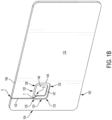
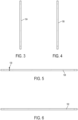
- Figs. 1A-7 show an exemplary transaction card or portion of a card 100, having a card periphery 101 defined by left side 104 (also depicted in FIG. 3 ), right side 106 (also depicted in FIG. 4 ), top side 108 (also depicted in FIG. 5 ), and bottom side 102 (also depicted in FIG. 6 ).
- Left side 104 and right side 106 are parallel to one another, and top side 108 and bottom side 102 are parallel to each other.
- Sides 104 and 106 may be referred to as the "relatively shorter" sides and sides 108 and 102 referred to as the "relatively longer" sides.
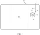
- 1C is a metal layer 100 having a front surface 112 (also depicted in FIG. 2 ) and a back surface 114 (also depicted in FIG. 7 ).
- front and back are used herein for differentiation of the opposite surfaces, and no particular significance is intended by the use of these terms.
- right and left and top and bottom are used to refer to the sides that form the periphery of the card, which terms are oriented from a view of the front surface of a card as depicted in, e.g., Fig. 2 , but again, this terminology is for ease of description only.
- side is used herein to refer to the sides that form periphery of the card
- edge is used to refer to the edges of the boundary of the opening, but the use of these terms is intended only for differentiation, without specific significance to the terminology used.
- an opening 120 in the metal layer 100 is sized to accommodate a transponder chip module 121 having a front surface 127 and a back surface 126 (as shown in FIG. 3 ).
- the details of the transponder chip module are not a claimed feature of the invention and are shown for illustrative purposes only. Although an 8-pin module is shown, the transponder may have fewer or more contacts, such as for example, a 6-pin module. Those of skill in the art will recognize that any number of different transponder chip designs are available and may be used in an exemplary card.
- the opening has a left edge 124 parallel and relatively closest to the left short side 104 of the card periphery 101, a second edge 128 parallel and relatively closest to the top side 108 of the card periphery, a third edge 122 parallel and relatively closest to the bottom side 102 of the card periphery.
- Left edge 124 is relatively closer to the left side 104 of the card periphery than the top edge 128 is to the top side 108 of the periphery
- the top edge 128 is relatively closer to the top side 108 of the periphery than the bottom edge 122 is to the bottom side 102 of the card periphery.
- the edges of the opening 120 define corners (e.g. a top left corner 125 formed by edge 124 and edge 128 and a bottom left corner 123 formed by edge 124 and edge 122).
- a discontinuity or slit 130 in metal layer 100 comprises a gap in the metal layer extending from the front surface 112 to the back surface 114 of the metal layer 100.
- the terms “discontinuity” and “slit” may be used interchangeably herein.
- the discontinuity defines a path from an origin (O) at the card periphery and terminating at a terminus (T) in the periphery of the opening.
- the terminus is located relatively closer to corner 125 than to the adjacent corner 123 defined by common edge 124.
- Most if not all of the other inventive embodiments depicted herein show the terminus located relatively closer to one corner than the other corner defined by the common edge. This is in contrast to prior art designs that depict the slit terminating in a location at a midpoint between adjacent corners 123 and 125.
- Opening 120 is a stepped pocket opening that defines an overall area having an outer boundary 144 and an inner boundary 146.
- An upper portion (open to the front surface of the card) of the stepped pocket opening has an open area defined by the outer boundary 144.
- a lower portion of the pocket (open to the back surface of the card) has an area defined by inner boundary 146, wherein the area of the lower portion of the pocket is less than the area of the upper portion of the pocket.
- the wall between the inner boundary and the outer boundary along the direction of the thickness of the card defines a ledge 147 between the inner boundary and wall of the upper pocket and having a surface parallel to the upper and lower surfaces of the card.
- parallel as used in connection with any and all comparative features is intended to mean parallel within a desired tolerance, but may include features that are not precisely parallel.
- the discontinuity is depicted as having an endpoint E located on the inner boundary 146.
- Fig. 1A depicts a "tool path and milling boundary view" of the card of FIGS. 1B and 1C .
- Fig. 1A schematically reflects discontinuity 130 as a line showing a tool path for the cutter (e.g. laser) for generating the discontinuity.
- the line 130 in FIG. 1A extends past the origin O on the periphery of the card and past the endpoint E on the inner boundary of the opening.
- the manufacturing boundary lines corresponding to the opening depict the locations of the inner boundary 146 and outer boundary 144 of the upper and lower pockets generated by the pocket-making process, which may be performed by milling tools, etching tools, lasers, and the like.
- the discontinuity may first be cut in the metal layer, such as with a laser, along a line including origin O and endpoint E and which may extend past both origin O and endpoint E to ensure a complete cut through the metal layer. Then the upper and lower pockets are milled.
- the discontinuity actually ends at the inner boundary 146 at point E, but from the front of the card as depicted in FIG. 1C , the discontinuity is only visible to the edge of the outer boundary 144 at point T, because of the payment module inserted in the opening.
- the discontinuity 130 extends to the endpoint E on the back of the card. It should be understood that the design of the transponder chip depicted herein only illustrates an exemplary contact pattern, and the invention is not limited to any particular pattern. It should also be understood that although the discontinuity 130, the inner boundary 146, and the back surface of the module 126 are depicted on the back of the metal layer in FIG. 7 , layers over the back surface of the card may fully or partially obscure visibility of the discontinuity, the transponder chip, and the opening, depending upon the nature and opacity of the back layer.
- the opening and transponder chip are typically obscured from view by an opaque member or portion of a layer, but some portion of the discontinuity may be detectible from the back side, if viewed closely and if an optional back layer of the card is not fully opaque.
- the contacts on the top surface 127 of the transponder module are preferably flush with the outermost front surface of the card. If the metal layer is the top layer, the contacts will be flush with the front surface of the metal layer. If another layer, such as a clear plastic layer or a ceramic layer, are disposed on top of the metal layer, however, such as depicted in FIG. 32 , the contacts will be mounted flush with the top layer 1200.
- the opening may be cut by first milling the lower portion and then milling the upper portion, or vice versa.
- the lower portion may be milled from the back surface of the card, and the upper portion from the front surface of the card (although both portions may be milled from the front surface).
- a non-conductive material may be provided in the opening by any of the methods described in U.S. Pat. No. 9.390,366 , incorporated herein by reference.
- acceptable ranges of performance may have X and Y dimensions preferably in the range of 7 mm to 10 mm, and more preferably in the range of 7.5 mm to 9.5 mm.
- the size of the gap in the discontinuity may also impact performance, with the gap size preferably less than 1 mm, more preferably less than 0.5 mm, and most preferably about 0.1 mm, plus or minus 0.05 mm.
- the invention is not limited to any particular discontinuity gap size or dimensions of the lower portion of the pocket, however.
- the left side 104 of the card has a region 150 (shown in FIG. 2 only, to reduce clutter) that is aligned with (e.g.
- the terminus is located at corner 125.
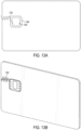
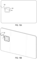
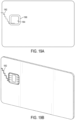
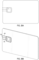
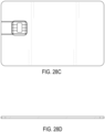
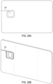
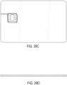
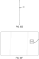
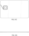
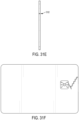
- FIGS. 8A-31A Depicted in FIGS. 8A-31A are various other slit configurations, each of which can be characterized in numerous ways and may have certain features.
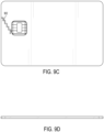
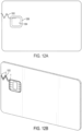
- Each Fig. 8A , 9A , etc. depicts the manufacturing path or boundary lines associated with each slit design.
- the line 802, 902, etc. corresponding to the slit as depicted corresponds to the tool path for the cutter (e.g. laser) for generating the discontinuity.
- the manufacturing boundary lines corresponding for the opening depicts the inner (e.g. 804, 904) and outer (e.g. 806, 906) boundaries of the upper and lower pockets generated by the pocket-making tools, which may be milling tools, etching tools, lasers, and the link.
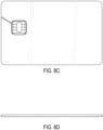
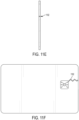
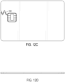
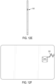
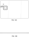
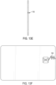
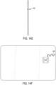
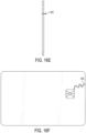
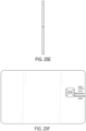
- FIGS. 8B-8F, 9B-9F , etc. depict the designs as shown in FIGS. 8B-8F, 9B-9F , etc., in which, for example, FIGS. 8B , 9B , etc. depict the front view perspective views of the metal layer of the respective cards, FIGS. 8C , 9C , etc. depict front surface views, FIGS. 8D , 9D , etc. depict top (or bottom) side views, FIGS. 8E , 9E , etc. depict left side views, and FIGS. 8F , 9F , etc. depict back surface views.
- the one of the top side view or bottom side view depicted is selected to show the side of the card on which the origin (O) of each discontinuity is located, whereas the one of the top or bottom side view not depicted is essentially identical to FIG. 6 .
- the right side view for all of the aforementioned embodiments is essentially identical to the side view depicted in FIG. 4 .
- FIGS. 8A-F to 31A-F depict only the metal layer of the exemplary cards.
- the metal layer may have one or more layers disposed over the front surface or the back surface of the card, and each additional layer may cover the entire surface or only a portion of the surface.
- the metal layer itself may comprise a composite of multiple metal layers, including embodiments in which at least one layer comprises a different metal than another.
- the additional layers may comprise, for example, any of the layers described in U.S. Published Pat. App. No. US20150339564A1 and/or US20170316300A1 , incorporated herein by reference in their entireties.
- a preferred embodiment may comprise a ceramic coating on the front surface of the metal card and a plastic layer on the back surface of the card.
- the origin (O) is located relatively closer to the line defined by the top side 108 than the terminus (T). This characterization is also true of the slit configuration depicted in FIG. 1 , in which the origin (O) is located on the top side 108.
- the location of the origin relatively closer to the line defined by the top side of the periphery than the terminus is also true of at least the designs depicted in FIGS. 9A , 10A , 12A , 14A-17A , 19A-21A , 30A , and 31A .
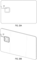
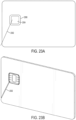
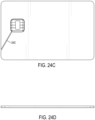
- the location of the terminus is located relatively closer to the line defined by the top side 108, such as in the slit designs depicted in FIGS. 22A-24A .
- the term "line defined by the top side” refers to the imaginary line in space along which the top side 108 lies. Because the cards have rounded corners, the distance from the origin to the line defined by top side 108 is measured from intersection of the line defined by the top side 108 and the line defined by the left side 104, which point is not actually physically present as part of a metal layer having standard rounded corners.
- one of the terminus or the origin are located relatively closer to one long side of the periphery than the other.
- the terminus and the origin may be located approximately the same distance from the top or bottom sides.
- the contacts may be located in a mirror image position on the lower back right of the card and provide equivalent functionality, with the discontinuity similarly located relative to the back surface of the card as depicted herein relative to the front surface.
- the "front” and “back” surfaces of the card are relative to the disposition of the transponder module and do not necessarily reflect a traditional "front” or “back” as those terms might be used by a consumer in receipt of the final card.
- the location of the contacts is dictated by the arrangement of card readers that read the cards via a physical connection, and it should be understood that the location of the transponder chip relative to the periphery of the card is not limited by the invention.
- the discontinuity path comprises at least two changes in direction of 90 degrees or more.
- Figs. 9A , 19A , and 31A illustrate stairstep designs in which the discontinuity path makes multiple 90 degree changes in direction.
- the stairstep geometry has a rise (vertical distance covered between adjacent horizontal sections) and a run (horizontal distance covered between adjacent vertical sections), in which the rise is greater than the run.
- the rise and run may be equal or the run may be greater than the rise.
- the rise and run are roughly equal for each step, but in other embodiments, the rise and run may be different in at least one step relative to others in the series of steps.
- FIG. 11A and 13A illustrate sawtooth geometries in which the path of the discontinuity makes multiple changes in direction of more than 90 degrees.
- FIG. 12A illustrates a discontinuity path that has a micro stairstep geometry and a macro sawtooth geometry, comprising at least a first plurality of more than two changes in direction of 90 degrees leading to a first change in direction of more than 90 degrees and a second plurality of more than two changes in direction of 90 degrees leading to a second change in direction of more than 90 degrees.
- each "tooth" in the sawtooth geometry of roughly equal dimension the invention is not limited to such geometries.
- the discontinuity path may also have at least one section of curved geometry.
- a basic curved geometry is illustrated in FIG. 10A , but the curved design may also have one or more changes in direction greater than or equal to 90 degrees, wherein at least one of the changes in direction has a curved geometry.
- the embodiments illustrated in FIGS. 14A-18A depict such features, with the discontinuity paths illustrated in FIG. 14A-16A each having a sinusoidal shape for at least a portion of the path comprising at least two changes in direction of more than 90 degrees.
- a curved path with multiple changes in direction may also have portions that complete a change in direction of more than 180 degrees before making a subsequent change in direction of more than 180 degrees, as depicted in FIGS. 17A-C .
- the size of each section encompassing a 180 degree change in direction may vary over the length of the path from a relatively smaller section 1712 to a relatively larger section 1714.
- the path in FIG. 31A depicts sections of curved geometry within a stairstep architecture, comprising a radius or fillet instead of a right angle for each change of direction of 90 degrees. Such a path may enable faster operation of the cutting tool and/or may be aesthetically more pleasing than the embodiment with sharp direction changes.
- the terminus of the discontinuity may be located on the top edge opening with the origin located on the left side of the card.
- the discontinuity may be located on the top or bottom side of the card periphery and the terminus may be on the top or bottom edge or a top or bottom corner of the opening.
- the discontinuity has a terminus located on the left edge of the opening at a location relatively closer to the bottom left corner 125 than the upper left corner 123 and has an origin in the left side of the card periphery in a location relatively closer to the upper left corner 123 than the bottom left corner 125.
- the terminus location is relatively closer to upper left corner 123 than the bottom left corner 125 and the origin is located in the left side of the card periphery relatively closer to the upper left corner 123 than the bottom left corner 125.
- the paths of the discontinuities for both of the foregoing types of embodiments are generally diagonal and downward from the origin to the terminus, but the first group terminates on the left edge of the opening closer to the bottom corner than the top corner.
- a transponder chip module 121 is disposed in the opening, and the metal layer serves as an amplifying antenna for the transponder chip module.
- the card may comprise at least one non-metal layer 1200, 1300 disposed on at least one surface of the metal layer 1100, such as but not limited to a plastic layer, a ceramic layer, a decorative layer comprising one of wood or leather, or a combination thereof.
- disposed does not denote a direct connection to the respective surface, but also an indirect connection (i.e. on top of one or more other layers that are directly connected to the surface).
- the card may have a front surface coated with ceramic layer 1200 and a back surface on which a plastic layer 1300 is attached, preferably by an adhesive.
- attachment of a plastic layer with an adhesive may comprise employing a carrier substrate (e.g. polyester) having adhesive (e.g. an ethylene copolymer adhesive, such as ethylene acrylic acid (EEA)) on both sides.
- a carrier substrate e.g. polyester
- adhesive e.g. an ethylene copolymer adhesive, such as ethylene acrylic acid (EEA)
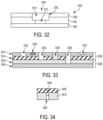
- the gap 3402 defined by the discontinuity may at least partially filled with the ceramic coating, leaving a surface imperfection 3404 still visible from the top surface of the ceramic coating.
- the discontinuity as described herein may be optically visible from one or both surfaces of the card.
- the discontinuity may not be visible from the back surface.
- the discontinuity may also be hidden from the front.
- the ceramic coating may only partially fill the gap caused by the discontinuity, thereby making the discontinuity still visibly perceptible, at least as a surface imperfection 3404 as depicted in Fig. 34 , which imperfection may be in the form of at least a perceptible line, if not a perceptible gap.
- that metal layer may be a top layer, or it may be a layer that is covered with another layer but still visibly perceptible in some way.
- the card may comprise a plurality of discontinuities, such as in the embodiments depicted in FIGS. 25A-28A .
- at least one of the plurality of discontinuities e.g. 2502, 2602, 2702, 2802
- at least two of the plurality of discontinuities e.g. 2502 and 2504, 2602 and 2604, etc.
- fewer than all of the plurality of discontinuities may extend from the periphery to the opening, meaning that one or more discontinuities (e.g.
- the presence of multiple discontinuities spreads the stress associated with flexure across multiple locations, minimizing the stress whitening attributable to any one discontinuity.
- metal areas disposed between such slits are held in place by the overlying and underlying non-metal layers of the card.
- a method for making a transaction card as described herein comprising the steps of (a) providing a metal layer having an front surface and a back surface; (b) creating an opening in the metal layer sized to accommodate a transponder chip module, having the features described herein, (c) creating a discontinuity in the metal layer as described herein, and (d) disposing the transponder chip module in the opening.
- the step of creating the discontinuity may precede the step of creating the opening for the transponder chip module.
- the method may comprise at least partially filling the gap defined by the discontinuity with a non-metal material, such as ceramic.
- the method may also further comprise disposing at least one non-metal layer on the front surface or the back surface of the metal layer, such as by adhesively bonding the non-metal layer to the metal layer, or by spray coating a ceramic layer onto the metal layer.
- the non-metal layer comprises a ceramic layer having a color, in which the method further comprises using a laser to create one or more permanent markings on the ceramic layer having a different color than the ceramic layer color, as described in more detail with respect to FIG. 33 later herein.
- the permanent markings in the ceramic may arise from a chemical change of a pigment within the ceramic composition, or the permanent markings may arise from removing an overlying ceramic layer to reveal an underlying layer having a different color.
- the underlying layer with the different color may comprise an underlying ceramic layer, if multiple layers of ceramic are provided.
- a white colored base ceramic layer having a white pigment therein may have better adhesion than a layer having a colored pigment, and therefore a first, white layer may be disposed underneath a second, non-white layer of ceramic.
- multiple ceramic layers may be used for aesthetic purposes.
- the exposed underlying layer having the different color may be the metal layer.
- a composite metal core may facilitate the appearance of different colors depending upon the depth of the engravings.
- the engraving may be performed by any method, such as a chemical or mechanical method, and is not limited to laser marking.
- grooves in the ceramic may be filled with another substance, such as metal.
- a ceramic-coated steel card may have laser engraved grooves in the ceramic coating that penetrate to the metal, and then a noble or precious metal, such as gold, silver, platinum, or the like, may be electroplated into the groove as a filler.
- the various configurations comprising the ceramic layers as described herein are not limited to card embodiments having a discontinuity in the metal layer as described herein.
- the ceramic layer may comprise one or more layers of a ceramic coating applied directly to the metal and cured, other methods of providing the ceramic layer may include adhering a freestanding monolithic ceramic layer to the metal layer or disposing a ceramic coating on a substrate, and then adhering the ceramic-coated substrate to the metal layer.
- a ceramic layer may be created by tapecasting and adhered to the body.
- Cards with slit geometries as shown and claimed herein have functional advantages over cards with straight slit geometries or other geometries of the prior art, per the examples noted herein. While all of the discontinuity designs may have functional advantages over prior art designs, some more than others, and all or most may have relatively similar production costs, some may be considered more aesthetically pleasing than others and thus may be favored purely for aesthetic reasons. Thus, certain features of the discontinuities in the metal layers disclosed herein may be selected for ornamental design and are not dictated by practical function. Accordingly, design elements of each may be varied and selected while maintaining functionality, such that a variety of ornamental configurations are available with substantially the same function or performance.
- the exact contours of the discontinuity may be varied to provide different ornamental appearances while maintaining substantially the same functionality.
- the ornamental design of the metal layer may be protected separately in one or more U.S. design patent applications.
- slit designs enable a traditional metal or ceramic-coated metal card to overcome potential weaknesses at the slit, which allow the card to maintain the traditional metal feel and sound.
- a self-supporting layer on the back of the card such as an FR4 material (a thermoset laminate made with epoxy resin and woven fiberglass) or polyimide.
- Printed layers such as for the various indicia, magnetic stripe, etc., may be assembled with the FR4 layer or printed directly on the FR4 layer.
- a relatively thin (e.g. 0.009 inches thick) stainless steel substrate 1100 may be used with an FR4 backing layer 1300.
- an 18 mil stainless steel layer may have on its back side a 4 mil FR4 layer (attached to the steel layer with a 2 mil adhesive layer), a 5 mil printed sheet on the back of the FR4 layer (attached via another 2 mil adhesive layer), and a 2 mil overlay layer comprising the magnetic stripe laminated to the back side of the print sheet layer.
- the print sheet and mag stripe overlay layers are the layers vulnerable to stress whitening, which the reinforcing layer helps to prevent.
- While reinforced backing may enable the weakness of the slit to be overcome sufficiently without a need to use one of the other slit designs described herein, embodiments combining both an FR4 (or other self-supporting) layer and one of the slit geometries depicted herein may also be provided.
- Preferable self-supporting layers have a rigidity of 80MPa ⁇ m 3 to 40 GPa ⁇ m 3 .
- FIG. 32 there is shown a cross-sectional illustration of an exemplary card embodiment 1000, showing the metal layer 1100, which may be any metal layer as described herein, with or without a slit, and having a stepped opening 1005 therein, including an opening upper portion 1010, the opening lower portion 1012. Also illustrated in FIG. 32 are a front layer 1200 and a back layer 1300. Layer 1200 has an opening 1205 that matches (i.e. is coextensive with) opening upper portion 1010, so that the contacts of a transponder module disposed in the opening in the metal card will sit relatively flush with the upper surface of layer 1200.
- the thicknesses of the layers depicted in any of the drawings herein are not to scale.
- the front layer as depicted in FIG. 32 may represent a plurality of layers
- the back layer as depicted may represent a plurality of layers
- the metal layer as depicted may represent a plurality of layers, or any combination thereof.
- Layers 1200 and 1300 are both optional.
- layer 1200 may comprise a 9 mil PVC or PVC/PEEK composite layer on the front of a 10 mil metal layer and a 10 mil PVC layer on the back of the metal layer.
- the front and back layers may each be adhered to the metal layer with 2 mil adhesive layers, such as a polyester substrate having EEA adhesive on both sides, as is well known in the art.
- the card may comprise a printable metal such as printable stainless steel having a coating at least on its front face that improves acceptance of printing inks on the stainless steel surface.
- the coating may comprise, for example, a polyester based coating receptive to UV curable screen and inkjet inks or solvent or oxidation printing.
- front layer 1200 comprises a ceramic layer (applied to the metal layer by any of the methods described herein) and back layer comprises a plastic layer.
- back layer 1200 may be a self-supporting layer, such as a layer made from FR4.
- a ceramic layer 3300 on a metal layer 3302 may comprise at least two ceramic layers 3312 and 3314, each layer having a different color.
- metal layer 3302 may comprise at least two metal layers 3322, 3324, and the two metal layers may be different metals having different colors.
- Creating a design in the ceramic layer may comprise making laser markings 3330 that change a color in the ceramic layer by permanently chemically changing a pigment in the ceramic layer, or by removing a portion of the ceramic to make a groove.
- Such a groove may be a superficial groove, such as groove 3331 that does not penetrate the upper layer to reveal underlying layers, or may be a groove that reveals an underlying layers.
- Grooves may be created with laser, mechanical, or chemical methods known in the art. Grooves that reveal an underlying layer may include grooves 3332 that remove one ceramic layer 3312 to reveal another ceramic layer 3314, grooves 3334 that remove all ceramic layers 3312 and 3314 to reveal an upper metal layer 3322, and grooves 3336 that remove all the ceramic layers 3312, 3314 and the upper metal layer 3322 to expose an underlying metal layer 3324. Still another design technique may include creating a groove (such as any of the groove embodiments described above) and then filling that groove in the ceramic with another material, such as an electroplated metal 3338, which may be a different metal than one or both of the other metal layer or layers.
- the initial groove is preferably a groove 3334 or 3336 that removes the ceramic down to a metal layer.
- each of the various grooves and marking techniques may be practiced alone or in any combination with others described herein.
- the various techniques for creating decorations in a ceramic card are not limited to such embodiments.
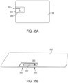
- Yet another embodiment of strengthening a section of a card having a discontinuity comprises providing a supporting tab overlying and/or underlying the discontinuity, such as for card 3500 depicted in FIGS. 35A-E .
- a supporting tab overlying and/or underlying the discontinuity, such as for card 3500 depicted in FIGS. 35A-E .
- pockets 3510, 3512 around the opening 3520 for the module are recessed in the Z axis on both sides of the card.
- Pockets 3510, 3512 on opposite sides of the card, both of which of which have an area that is less than the area of the metal layer, are depicted as the same size as one another in the figures, but can be different sizes.
- Non-metal inserts 3540, 3550 are placed into the pockets 3510, 3512.
- a pocket and corresponding insert may be provided only in the front.
- Front insert 3540 has a hole 3545 to accommodate the module and expose the contact portion of the module on the top surface of the card.
- an insert construction such as is disclosed herein, may avoid the need to provide a stepped pocket for the transponder module in the metal layer, as the thicknesses of the pockets on either side may be selected so that the "lip" (larger periphery portion) of the module (not shown) rests on the shelf created by the card body and the portion on the back of the module protrudes through the hole 3520 in card body and stops short of the inner surface of the rear insert 3550.
- Artwork may be applied to the inserts by laser or any means known in the art.
- any of the methods disclosed herein for strengthening an area around a discontinuity of a card may be practiced alone or in combination with one another, and that, for example, the use of additional .
- Any other methods of creating designs or providing indicia on card as are well known in the art may also be provided, including providing a signature block, a magnetic stripe, a hologram, branding indicia, personalization information, and the like.
- Exemplary slit design embodiments as depicted herein showed less ink cracking substrate stress whitening after short dimension bending (bending parallel to the long edges) than other cards, when subjected to a Dynamic Bending Stress Test (ref ISO/IEC 10373-1:2006).
- Various embodiments were tested up to 500 Flex Test Cycles at a rate of 30 cycles/minute per axis. Design (by reference to Fig. # where depicted) Bend Cycles Across Short Axis Before Stress Whitening Induced Linear near center of chip cavity Immediate Fig 29 ⁇ 50 Fig. 1 >50 Fig. 23 >250 Fig 19 >250 Fig. 9 >500 Fig. 15 >500
- discontinuity geometries shown herein have functional advantages over prior art geometries, it should be understood that there are potentially an infinite variety of geometries available, and that those depicted herein are merely a small subset of the myriad geometries available that conform to the claims.
- myriad geometries available including the myriad variations of a particular geometry, which may exhibit suitable performance and function, there may be certain designs that are preferred for purely aesthetic reasons. Accordingly, inclusion of any specific design herein representative of a particular geometry is not an indication that the specific design is functionally better than an alternative design of a similar or even a different geometry, except as specifically noted.
- the number of directional changes after a threshold number may be selected primarily for aesthetic reasons. Accordingly, the description herein is provided without prejudice to any number of design patent applications relating to the specific designs presented herein. Features shown in solid lines in the utility patent drawings herein are without prejudice to showing the same in dashed lines to signify their non-inclusion within the scope of the design patent claims. In particular, one or more features visible on the back surfaces of the metal layer embodiments depicted herein may or may not be visible in a completed card, because of one or more overlying layers and thus may be depicted in dashed lines when depicting claimed design attributes, to show that such features are not claimed. Similarly, the details of the transponder module contacts are not a claimed aspect of the invention, and may be depicted in dashed lines in any drawing depicting claimed design attributes.
Landscapes
- Engineering & Computer Science (AREA)
- Physics & Mathematics (AREA)
- General Physics & Mathematics (AREA)
- Theoretical Computer Science (AREA)
- Microelectronics & Electronic Packaging (AREA)
- Computer Hardware Design (AREA)
- Computer Networks & Wireless Communication (AREA)
- Credit Cards Or The Like (AREA)
- Laminated Bodies (AREA)
- Fixed Capacitors And Capacitor Manufacturing Machines (AREA)
- Electrochromic Elements, Electrophoresis, Or Variable Reflection Or Absorption Elements (AREA)
- Burglar Alarm Systems (AREA)
- Semiconductor Integrated Circuits (AREA)
Applications Claiming Priority (5)
| Application Number | Priority Date | Filing Date | Title |
|---|---|---|---|
| US201862623936P | 2018-01-30 | 2018-01-30 | |
| US15/928,813 US10762412B2 (en) | 2018-01-30 | 2018-03-22 | DI capacitive embedded metal card |
| EP23162791.0A EP4220483B1 (de) | 2018-01-30 | 2019-01-23 | Kapazitive eingebettete metallkarte mit doppelschnittstelle |
| EP19747736.7A EP3746943B1 (de) | 2018-01-30 | 2019-01-23 | Kapazitive eingebettete doppelschnittstellen-metallkarte |
| PCT/US2019/014656 WO2019152235A1 (en) | 2018-01-30 | 2019-01-23 | Dual interface capacitive embedded metal card |
Related Parent Applications (2)
| Application Number | Title | Priority Date | Filing Date |
|---|---|---|---|
| EP19747736.7A Division EP3746943B1 (de) | 2018-01-30 | 2019-01-23 | Kapazitive eingebettete doppelschnittstellen-metallkarte |
| EP23162791.0A Division EP4220483B1 (de) | 2018-01-30 | 2019-01-23 | Kapazitive eingebettete metallkarte mit doppelschnittstelle |
Publications (2)
| Publication Number | Publication Date |
|---|---|
| EP4567664A2 true EP4567664A2 (de) | 2025-06-11 |
| EP4567664A3 EP4567664A3 (de) | 2026-02-11 |
Family
ID=67392231
Family Applications (3)
| Application Number | Title | Priority Date | Filing Date |
|---|---|---|---|
| EP23162791.0A Active EP4220483B1 (de) | 2018-01-30 | 2019-01-23 | Kapazitive eingebettete metallkarte mit doppelschnittstelle |
| EP25173390.3A Pending EP4567664A3 (de) | 2018-01-30 | 2019-01-23 | Kapazitive eingebettete metallkarte mit doppelschnittstelle |
| EP19747736.7A Active EP3746943B1 (de) | 2018-01-30 | 2019-01-23 | Kapazitive eingebettete doppelschnittstellen-metallkarte |
Family Applications Before (1)
| Application Number | Title | Priority Date | Filing Date |
|---|---|---|---|
| EP23162791.0A Active EP4220483B1 (de) | 2018-01-30 | 2019-01-23 | Kapazitive eingebettete metallkarte mit doppelschnittstelle |
Family Applications After (1)
| Application Number | Title | Priority Date | Filing Date |
|---|---|---|---|
| EP19747736.7A Active EP3746943B1 (de) | 2018-01-30 | 2019-01-23 | Kapazitive eingebettete doppelschnittstellen-metallkarte |
Country Status (18)
| Country | Link |
|---|---|
| US (12) | US10762412B2 (de) |
| EP (3) | EP4220483B1 (de) |
| JP (1) | JP6974621B2 (de) |
| KR (1) | KR102355471B1 (de) |
| CN (2) | CN111684466B (de) |
| AU (1) | AU2019213838B2 (de) |
| CA (6) | CA3088900C (de) |
| CO (1) | CO2020009063A2 (de) |
| DK (2) | DK3746943T3 (de) |
| ES (2) | ES3037302T3 (de) |
| FI (2) | FI4220483T3 (de) |
| HU (2) | HUE072144T2 (de) |
| MX (1) | MX385703B (de) |
| PL (2) | PL3746943T3 (de) |
| PT (2) | PT3746943T (de) |
| SG (1) | SG11202006484SA (de) |
| WO (1) | WO2019152235A1 (de) |
| ZA (1) | ZA202004153B (de) |
Families Citing this family (45)
| Publication number | Priority date | Publication date | Assignee | Title |
|---|---|---|---|---|
| US11551051B2 (en) * | 2013-01-18 | 2023-01-10 | Amatech Group Limiied | Coupling frames for smartcards with various module opening shapes |
| US11341389B2 (en) | 2013-01-18 | 2022-05-24 | Amatech Group Limited | Manufacturing metal inlays for dual interface metal cards |
| US11354558B2 (en) * | 2013-01-18 | 2022-06-07 | Amatech Group Limited | Contactless smartcards with coupling frames |
| US11354560B2 (en) | 2013-01-18 | 2022-06-07 | Amatech Group Limited | Smartcards with multiple coupling frames |
| US11928537B2 (en) | 2013-01-18 | 2024-03-12 | Amatech Group Limited | Manufacturing metal inlays for dual interface metal cards |
| US10977540B2 (en) | 2016-07-27 | 2021-04-13 | Composecure, Llc | RFID device |
| US11618191B2 (en) | 2016-07-27 | 2023-04-04 | Composecure, Llc | DI metal transaction devices and processes for the manufacture thereof |
| US10762412B2 (en) | 2018-01-30 | 2020-09-01 | Composecure, Llc | DI capacitive embedded metal card |
| US11267172B2 (en) | 2016-07-27 | 2022-03-08 | Composecure, Llc | Overmolded electronic components for transaction cards and methods of making thereof |
| SG11202002064SA (en) | 2017-09-07 | 2020-04-29 | Composecure Llc | Transaction card with embedded electronic components and process for manufacture |
| US11151437B2 (en) | 2017-09-07 | 2021-10-19 | Composecure, Llc | Metal, ceramic, or ceramic-coated transaction card with window or window pattern and optional backlighting |
| HUE060022T2 (hu) | 2017-10-18 | 2023-01-28 | Composecure Llc | Fém, kerámia vagy kerámiabevonatos tranzakciókártya ablakkal vagy ablakmintával és opcionális háttévilágítással |
| US11361204B2 (en) | 2018-03-07 | 2022-06-14 | X-Card Holdings, Llc | Metal card |
| USD971211S1 (en) * | 2018-07-23 | 2022-11-29 | Samsung Display Co., Ltd. | Display module |
| USD956760S1 (en) * | 2018-07-30 | 2022-07-05 | Lion Credit Card Inc. | Multi EMV chip card |
| USD880584S1 (en) | 2018-09-17 | 2020-04-07 | Apple Inc. | Label |
| US11347993B2 (en) | 2019-08-12 | 2022-05-31 | Federal Card Services, LLC | Dual interface metal cards and methods of manufacturing |
| US12277462B2 (en) | 2019-08-14 | 2025-04-15 | Federal Card Services, LLC | Metal-containing dual interface smartcards |
| US11113593B2 (en) | 2019-08-15 | 2021-09-07 | Federal Card Services; LLC | Contactless metal cards with fingerprint sensor and display |
| US11416728B2 (en) | 2019-08-15 | 2022-08-16 | Federal Card Services, LLC | Durable dual interface metal transaction cards |
| USD937929S1 (en) * | 2019-08-19 | 2021-12-07 | Visa International Service Association | Transaction card |
| US11455507B2 (en) | 2019-10-13 | 2022-09-27 | Federal Card Services, LLC | Metal transaction cards containing ceramic having selected coloring and texture |
| TWI856170B (zh) | 2019-10-25 | 2024-09-21 | 美商坎柏斯庫爾有限責任公司 | 具生物特徵之金屬卡片 |
| WO2021097208A1 (en) * | 2019-11-16 | 2021-05-20 | Federal Card Services, LLC | Rfid enabled metal transaction card with shaped opening and shaped slit |
| EP4028947A4 (de) * | 2019-11-16 | 2024-01-24 | Federal Card Services, LLC | Rfid-aktivierte metalltransaktionskarte mit geformter öffnung und geformtem schlitz |
| US11341385B2 (en) | 2019-11-16 | 2022-05-24 | Federal Card Services, LLC | RFID enabled metal transaction card with shaped opening and shaped slit |
| USD1032613S1 (en) * | 2020-02-02 | 2024-06-25 | Federal Card Services, LLC | Smart card |
| TWI804805B (zh) * | 2020-02-07 | 2023-06-11 | 美商坎柏斯庫爾有限責任公司 | 雙接口金屬交易裝置及其製程 |
| EP3889837A1 (de) * | 2020-04-01 | 2021-10-06 | Thales Dis France Sa | Radiofrequenz-chipkarte und verfahren zu ihrer herstellung |
| USD948613S1 (en) | 2020-04-27 | 2022-04-12 | Composecure, Llc | Layer of a transaction card |
| AU2021283041B2 (en) | 2020-06-01 | 2024-03-07 | Composecure, Llc | Transaction cards with discontinuous metal strata |
| TWI810690B (zh) | 2020-10-30 | 2023-08-01 | 美商坎柏斯庫爾有限責任公司 | 具有部分玻璃層之交易卡 |
| AU2022205660B2 (en) | 2021-01-08 | 2024-07-25 | Arculus Holdings, Llc | Devices, systems, and methods for public/private key authentication |
| DE102021000335A1 (de) * | 2021-01-22 | 2022-07-28 | Giesecke+Devrient Mobile Security Gmbh | Kartenkörper für eine Chipkarte und Chipkarte |
| US12321801B2 (en) * | 2021-09-06 | 2025-06-03 | Metaland Llc | Encapsulating a metal inlay with thermosetting resin and method for making a metal transaction card |
| US12427735B1 (en) * | 2021-09-06 | 2025-09-30 | Metaland Llc | Plating and coating of RFID enabled metal transaction cards with mechanically engraved and laser etched features |
| WO2023034642A1 (en) | 2021-09-06 | 2023-03-09 | Metaland Llc | Encapsulating a metal inlay with thermosetting resin and method for making a metal transaction card |
| US12481843B1 (en) * | 2021-09-06 | 2025-11-25 | Metaland Llc | Encapsulating a metal inlay with thermosetting resin and method for making a metal transaction card |
| JP7757665B2 (ja) * | 2021-09-08 | 2025-10-22 | Toppanホールディングス株式会社 | メタルカード |
| US12159180B1 (en) | 2021-11-29 | 2024-12-03 | Metaland Llc | RFID enabled metal transaction cards with coupler coil couplings and related methods |
| US12124905B1 (en) * | 2021-12-17 | 2024-10-22 | Wells Fargo Bank, N.A. | Transaction instrument with features for destruction and disposal |
| CN116666947A (zh) * | 2022-02-28 | 2023-08-29 | 深圳富泰宏精密工业有限公司 | 天线结构及具有该天线结构的穿戴式装置 |
| DE102022001595A1 (de) * | 2022-05-06 | 2023-11-09 | Giesecke+Devrient ePayments GmbH | Kartenförmiger Datenträger umfassend Keramik |
| AR134306A1 (es) | 2023-10-23 | 2026-01-07 | Arculus Holdings Llc | Sistemas, métodos y dispositivos para realizar transacciones de moneda fiduciaria y criptomoneda |
| EP4592892A1 (de) | 2024-01-23 | 2025-07-30 | Giesecke+Devrient ePayments America, Inc. | Metallisches kernelement, chipkartenkörper und verfahren zur herstellung einer chipkarte |
Citations (6)
| Publication number | Priority date | Publication date | Assignee | Title |
|---|---|---|---|---|
| US8608082B2 (en) | 2010-07-20 | 2013-12-17 | Oberthur Technologies | Microcircuit device including means for amplifying the gain of an antenna |
| US8725589B1 (en) | 2009-07-30 | 2014-05-13 | Jpmorgan Chase Bank, N.A. | Methods for personalizing multi-layer transaction cards |
| US20150339564A1 (en) | 2014-05-22 | 2015-11-26 | John Herslow | Transaction and id cards having selected texture and coloring |
| US9390366B1 (en) | 2015-07-08 | 2016-07-12 | Composecure, Llc | Metal smart card with dual interface capability |
| US20170316300A1 (en) | 2014-11-03 | 2017-11-02 | Composecure Llc | Ceramic-containing and ceramic composite transaction cards |
| US9812782B2 (en) | 2011-08-08 | 2017-11-07 | Féinics Amatech Teoranta | Coupling frames for RFID devices |
Family Cites Families (232)
| Publication number | Priority date | Publication date | Assignee | Title |
|---|---|---|---|---|
| US82A (en) | 1836-11-17 | Spiral bit with countersink for setting screws | ||
| US3802101A (en) | 1972-02-03 | 1974-04-09 | Transaction Technology Inc | Coded identification card |
| JPS54116043U (de) | 1978-02-01 | 1979-08-14 | ||
| CA1137641A (en) | 1979-06-22 | 1982-12-14 | Merle E. Homan | Single chip microcomputer selectively operable in response to instructions stored on the computer chip or in response to instructions stored external to the chip |
| DE3248385A1 (de) | 1982-12-28 | 1984-06-28 | GAO Gesellschaft für Automation und Organisation mbH, 8000 München | Ausweiskarte mit integriertem schaltkreis |
| JPS59228743A (ja) | 1983-06-10 | 1984-12-22 | Kyodo Printing Co Ltd | Icカ−ド用icモジユ−ル |
| JPS61222715A (ja) | 1985-03-28 | 1986-10-03 | Mitsubishi Electric Corp | 樹脂成形体の製造方法 |
| FR2579799B1 (fr) | 1985-03-28 | 1990-06-22 | Flonic Sa | Procede de fabrication de cartes a memoire electronique et cartes obtenues suivant ledit procede |
| JPS6244499A (ja) | 1985-08-22 | 1987-02-26 | 日本タングステン株式会社 | 識別カ−ド |
| JPS6399995A (ja) | 1986-05-23 | 1988-05-02 | 株式会社リコー | Icカ−ド及びその製造方法 |
| FR2599893B1 (fr) | 1986-05-23 | 1996-08-02 | Ricoh Kk | Procede de montage d'un module electronique sur un substrat et carte a circuit integre |
| JPS6372596A (ja) | 1986-09-17 | 1988-04-02 | 大日本印刷株式会社 | Icカ−ドの製造方法 |
| FR2609821B1 (fr) | 1987-01-16 | 1989-03-31 | Flonic Sa | Procede de realisation de cartes a memoire et cartes obtenues par la mise en oeuvre dudit procede |
| JPS63185688A (ja) | 1987-01-29 | 1988-08-01 | 大日本印刷株式会社 | Icカ−ドの製造方法 |
| US4808467A (en) | 1987-09-15 | 1989-02-28 | James River Corporation Of Virginia | High strength hydroentangled nonwoven fabric |
| JPH0633020B2 (ja) | 1988-03-04 | 1994-05-02 | シチズン時計株式会社 | 樹脂封止方法 |
| JPH0255198A (ja) | 1988-08-19 | 1990-02-23 | Mitsubishi Electric Corp | Icカード |
| JPH0289698A (ja) | 1988-09-27 | 1990-03-29 | Tdk Corp | 薄型電子機器 |
| CA2027823C (en) | 1989-10-31 | 1994-11-08 | Tomoshige Oka | Ic card having an integrated circuit module and air discharge opening |
| DE4038126C2 (de) | 1990-11-27 | 1993-12-16 | Mannesmann Ag | Verfahren und Vorrichtung zur Herstellung einer dekorierten Chip-Karte |
| DE59205116D1 (de) | 1991-05-10 | 1996-02-29 | Gao Ges Automation Org | Verfahren und vorrichtung zum herstellen von kunststoff-formstücken mit bereichsweise reduzierter wandstärke |
| JP3024838B2 (ja) | 1991-09-06 | 2000-03-27 | 大日本印刷株式会社 | 貴金属封入カード |
| FR2684235B1 (fr) | 1991-11-25 | 1999-12-10 | Gemplus Card Int | Carte a circuit integre comprenant des moyens de protection du circuit integre. |
| DE4142409A1 (de) | 1991-12-20 | 1993-07-01 | Gao Ges Automation Org | Verfahren zum bedrucken von karten mit sacklochfoermiger aussparung und vorrichtung zur ausfuehrung des verfahrens |
| US6817532B2 (en) | 1992-02-12 | 2004-11-16 | Lenscard U.S., Llc | Wallet card with built-in light |
| FR2716281B1 (fr) | 1994-02-14 | 1996-05-03 | Gemplus Card Int | Procédé de fabrication d'une carte sans contact. |
| JPH08123928A (ja) | 1994-10-26 | 1996-05-17 | Dainippon Printing Co Ltd | Ic付き光カード |
| JPH08123926A (ja) | 1994-10-26 | 1996-05-17 | Hitachi Maxell Ltd | 情報記憶担体及びその製造方法 |
| DE4446369A1 (de) | 1994-12-23 | 1996-06-27 | Giesecke & Devrient Gmbh | Datenträger mit einem elektronischen Modul |
| JPH08276459A (ja) | 1995-04-06 | 1996-10-22 | Dainippon Printing Co Ltd | 非接触icカード及びその製造方法 |
| FR2735714B1 (fr) | 1995-06-21 | 1997-07-25 | Schlumberger Ind Sa | Procede pour imprimer un graphisme sur une carte a memoire |
| USD405450S (en) | 1995-12-11 | 1999-02-09 | Sony Corporation | Speaker box |
| JPH09311921A (ja) | 1996-05-21 | 1997-12-02 | Oki Electric Ind Co Ltd | 回路基板及びそれを用いたicカード |
| JPH09315058A (ja) | 1996-05-30 | 1997-12-09 | Mitsubishi Electric Corp | Icカード |
| JPH09315053A (ja) | 1996-05-31 | 1997-12-09 | Yushi Seihin Kk | 識別体及びその製造方法 |
| DE19632113C1 (de) | 1996-08-08 | 1998-02-19 | Siemens Ag | Chipkarte, Verfahren zur Herstellung einer Chipkarte und Halbleiterchip zur Verwendung in einer Chipkarte |
| WO1998009252A1 (de) | 1996-08-26 | 1998-03-05 | Tomas Meinen | Verfahren zur herstellung von chipkarten |
| BE1010587A6 (nl) | 1996-08-28 | 1998-11-03 | Laureyssens Dirk | Electronisch sleutel-systeem. |
| ATE210864T1 (de) | 1996-10-09 | 2001-12-15 | Pav Card Gmbh | Verfahren und verbindungsanordnung zum herstellen einer chipkarte |
| JPH10162111A (ja) | 1996-11-29 | 1998-06-19 | Stanley Electric Co Ltd | Icカード |
| DE19703122C1 (de) | 1997-01-29 | 1998-05-20 | Orga Kartensysteme Gmbh | Verfahren zur Herstellung von Datenträgern |
| JPH10291392A (ja) | 1997-04-18 | 1998-11-04 | Dainippon Printing Co Ltd | Icカード |
| JPH1111056A (ja) | 1997-06-23 | 1999-01-19 | Nec Yamagata Ltd | Icカード |
| JPH11144014A (ja) | 1997-11-10 | 1999-05-28 | Hitachi Ltd | 非接触icカード |
| FR2783948B1 (fr) | 1998-09-24 | 2000-11-10 | Gemplus Card Int | Carte a puce grand format comprenant une mini-carte detachable et procede de fabrication |
| DE19848193C1 (de) | 1998-10-20 | 1999-11-11 | Orga Kartensysteme Gmbh | Trägerkarte für Miniaturchipkarte |
| DE19848712A1 (de) | 1998-10-22 | 2000-04-27 | Henkel Kgaa | Komponentenschicht für Smart Cards aus Schmelzklebstoffen |
| DE19934434B4 (de) | 1999-07-22 | 2006-10-05 | Bundesdruckerei Gmbh | Wert- und Sicherheitserzeugnis mit Mikrokanälen |
| US6492717B1 (en) | 1999-08-03 | 2002-12-10 | Motorola, Inc. | Smart card module and method of assembling the same |
| TW431033B (en) * | 1999-09-03 | 2001-04-21 | Ind Tech Res Inst | Twin-notch loaded type microstrip antenna |
| JP2001155275A (ja) | 1999-11-29 | 2001-06-08 | Nippon Signal Co Ltd:The | 外出設定方式 |
| JP2001216486A (ja) | 2000-02-04 | 2001-08-10 | Hitachi Ltd | Icカード表示装置 |
| FR2811109B1 (fr) | 2000-06-29 | 2002-12-27 | A S K | Objet portable sans contact comportant un ou plusieurs dispositifs peripheriques sans contact |
| US6759743B2 (en) | 2000-09-11 | 2004-07-06 | Xytrans, Inc. | Thick film millimeter wave transceiver module |
| US6923378B2 (en) | 2000-12-22 | 2005-08-02 | Digimarc Id Systems | Identification card |
| JP2002203215A (ja) | 2000-12-28 | 2002-07-19 | Dainippon Printing Co Ltd | 光コンピュータを有する表示カード |
| FR2826154B1 (fr) | 2001-06-14 | 2004-07-23 | A S K | Carte a puce sans contact avec un support d'antenne et un support de puce en materiau fibreux |
| DE10132893B4 (de) | 2001-07-06 | 2014-02-27 | Giesecke & Devrient Gmbh | Verfahren zum Einbau eines Displayelements |
| US6629969B2 (en) | 2001-07-26 | 2003-10-07 | Durect Corporation | Catheter for modification of agent formulation |
| US20030046555A1 (en) | 2001-08-31 | 2003-03-06 | Bradley Shawn J. | Identity verification using biometrics |
| JP2003087044A (ja) | 2001-09-12 | 2003-03-20 | Mitsubishi Materials Corp | Rfid用アンテナ及び該アンテナを備えたrfidシステム |
| JP2003234615A (ja) * | 2002-02-06 | 2003-08-22 | Nec Corp | スロットアンテナ及び無線lanカード |
| US20050087609A1 (en) | 2002-04-30 | 2005-04-28 | Tagsys, A Corporation Of France | Contactless label and method for its manufacture |
| JP2004094561A (ja) | 2002-08-30 | 2004-03-25 | Toppan Printing Co Ltd | Icカード |
| EP1437683B1 (de) | 2002-12-27 | 2017-03-08 | Semiconductor Energy Laboratory Co., Ltd. | Chipkarte und Buchhaltungssystem unter Verwendung der Chipkarte |
| US7823777B2 (en) | 2003-01-03 | 2010-11-02 | American Express Travel Related Services Company, Inc. | Metal-containing transaction card and method of making same |
| US7588184B2 (en) | 2003-01-03 | 2009-09-15 | American Express Travel Related Services Company, Inc. | Metal-containing transaction card and method of making the same |
| JP2004252802A (ja) | 2003-02-21 | 2004-09-09 | Konica Minolta Holdings Inc | 電子情報記録カード及びその製造方法 |
| US7566001B2 (en) | 2003-08-29 | 2009-07-28 | Semiconductor Energy Laboratory Co., Ltd. | IC card |
| US7762470B2 (en) | 2003-11-17 | 2010-07-27 | Dpd Patent Trust Ltd. | RFID token with multiple interface controller |
| US7597250B2 (en) | 2003-11-17 | 2009-10-06 | Dpd Patent Trust Ltd. | RFID reader with multiple interfaces |
| US7721956B2 (en) | 2003-12-10 | 2010-05-25 | American Express Travel Related Services Company, Inc. | Foldable transaction card systems |
| JP4939757B2 (ja) | 2004-02-04 | 2012-05-30 | 株式会社半導体エネルギー研究所 | Idラベル、idタグ及びidカード |
| USD507298S1 (en) | 2004-06-03 | 2005-07-12 | American Express Travel Related Services Company, Inc. | Card with an antenna and a rectangle |
| CN100352406C (zh) | 2004-08-17 | 2007-12-05 | 微创医疗器械(上海)有限公司 | 组合式可任意方向弯曲的覆膜支架 |
| US7237724B2 (en) | 2005-04-06 | 2007-07-03 | Robert Singleton | Smart card and method for manufacturing a smart card |
| CN101401492A (zh) | 2005-04-11 | 2009-04-01 | 艾维索股份有限公司 | 带定时器的分层标签结构 |
| EP1882229B1 (de) | 2005-04-27 | 2014-07-23 | Privasys, Inc. | Elektronische karten und herstellungsverfahren dafür |
| JP4715348B2 (ja) | 2005-07-14 | 2011-07-06 | 凸版印刷株式会社 | カード |
| DE102005039320A1 (de) | 2005-08-19 | 2007-02-22 | Giesecke & Devrient Gmbh | Kartenförmiger Datenträger |
| EP1760828A1 (de) | 2005-08-31 | 2007-03-07 | Incard SA | Kontaktlose Vorrichtung mit integriertem Schaltkreis |
| TWI283549B (en) | 2005-09-30 | 2007-07-01 | Univision Technology Inc | Organic electroluminescent display device with improved color saturation and method of fabricating the same |
| US7309007B2 (en) | 2005-10-04 | 2007-12-18 | First Data Corporation | Systems and methods for personalizing transaction cards |
| US20070080360A1 (en) | 2005-10-06 | 2007-04-12 | Url Mirsky | Microelectronic interconnect substrate and packaging techniques |
| US8786510B2 (en) | 2006-01-24 | 2014-07-22 | Avery Dennison Corporation | Radio frequency (RF) antenna containing element and methods of making the same |
| WO2007091638A1 (ja) | 2006-02-09 | 2007-08-16 | Sumco Techxiv Corporation | サセプタおよびエピタキシャルウェハの製造装置 |
| JP5034371B2 (ja) | 2006-02-10 | 2012-09-26 | 富士通株式会社 | Rfidタグの製造方法およびrfidタグ |
| CN101473338B (zh) | 2006-06-19 | 2012-06-06 | 纳格雷德股份有限公司 | 制造每一个均包括电子模块的卡和中间产品的方法 |
| US20070290048A1 (en) | 2006-06-20 | 2007-12-20 | Innovatier, Inc. | Embedded electronic device and method for manufacturing an embedded electronic device |
| JP2008009881A (ja) | 2006-06-30 | 2008-01-17 | Fujitsu Ltd | Rfidタグ製造方法およびrfidタグ |
| JP4855849B2 (ja) | 2006-06-30 | 2012-01-18 | 富士通株式会社 | Rfidタグの製造方法、およびrfidタグ |
| JP5078478B2 (ja) | 2006-07-28 | 2012-11-21 | 株式会社半導体エネルギー研究所 | 半導体装置 |
| US7838976B2 (en) | 2006-07-28 | 2010-11-23 | Semiconductor Energy Laboratory Co., Ltd. | Semiconductor device having a semiconductor chip enclosed by a body structure and a base |
| JP5027481B2 (ja) * | 2006-11-06 | 2012-09-19 | 株式会社日立製作所 | Icタグ |
| US9107336B2 (en) | 2007-02-09 | 2015-08-11 | Nagraid S.A. | Method of fabricating electronic cards including at least one printed pattern |
| WO2008105582A1 (en) | 2007-02-27 | 2008-09-04 | Gk Power Co., Ltd. | Credit card combined with decorations |
| KR101117921B1 (ko) | 2007-03-19 | 2012-06-20 | 나그라아이디 에스.에이. | 디지털 디스플레이를 포함하는 카드 |
| DE102007016777B4 (de) | 2007-04-04 | 2018-11-22 | Bundesdruckerei Gmbh | Sicherheits- oder Wertdokument |
| US8174454B2 (en) | 2007-05-07 | 2012-05-08 | Infineon Technologies Ag | Dual-band antenna |
| KR101237107B1 (ko) | 2007-09-14 | 2013-02-25 | 도판 인사츠 가부시키가이샤 | 안테나 시트, 트랜스폰더 및 책자체 |
| JP5037286B2 (ja) | 2007-09-28 | 2012-09-26 | 富士通株式会社 | Rfidタグおよびrfidタグの製造方法 |
| JP2009098871A (ja) | 2007-10-16 | 2009-05-07 | Seiko Epson Corp | Icカード |
| US8226013B2 (en) | 2007-10-26 | 2012-07-24 | Mastercard International, Inc. | Method and apparatus for use in providing an identification token |
| JP2009125995A (ja) | 2007-11-21 | 2009-06-11 | Konica Minolta Medical & Graphic Inc | カード及びicカード |
| USD573182S1 (en) | 2008-01-02 | 2008-07-15 | Target Brands, Inc. | Financial transaction card |
| US8141786B2 (en) | 2008-01-18 | 2012-03-27 | Texas Instruments Incorporated | Thin smart card module having strap on carrier |
| CN100576244C (zh) | 2008-05-27 | 2009-12-30 | 北京海升天达科技有限公司 | 智能卡及其制造方法 |
| DE102008027771A1 (de) | 2008-06-11 | 2009-12-17 | Giesecke & Devrient Gmbh | Verfahren zum Einbauen eines Chipmoduls in einen Chipkartenkörper |
| DE102008053582B3 (de) | 2008-10-28 | 2010-04-22 | Giesecke & Devrient Gmbh | Datenträger und Verfahren zu dessen Herstellung |
| DE102009015579A1 (de) | 2009-03-30 | 2010-10-07 | Soheil Hamedani | Münze mit integrierter RFID-Identifiziervorrichtung und Verfahren zu dessen Herstellung |
| EP2424041B1 (de) | 2009-04-21 | 2018-11-21 | Murata Manufacturing Co., Ltd. | Antennenvorrichtung und resonanzfrequenz-einstellverfahren dafür |
| USD632735S1 (en) | 2009-06-30 | 2011-02-15 | Cpi Card Group, Inc. | Clear single laminate transaction or access card with wood veneer layer |
| FR2948796A1 (fr) | 2009-07-28 | 2011-02-04 | Ask Sa | Support de dispositif d'identification radiofrequence pour carte hybride et son procede de fabrication |
| US8393547B2 (en) | 2009-08-05 | 2013-03-12 | Perfect Plastic Printing Corporation | RF proximity financial transaction card having metallic foil layer(s) |
| US20110031311A1 (en) | 2009-08-10 | 2011-02-10 | Outsite Networks, Inc. | Keyfob and in store device based promotion generation system and method |
| EP2302567B1 (de) | 2009-09-17 | 2015-11-11 | Nxp B.V. | Oberflächentolerante RFID-Transpondervorrichtung |
| US8128000B2 (en) | 2009-09-25 | 2012-03-06 | Avery Dennison Corporation | Method, system and apparatus for manufacturing a radio frequency identification device |
| DE102009043587A1 (de) | 2009-09-30 | 2011-05-19 | Smartrac Ip B.V. | Funktionelles Laminat |
| TWI449003B (zh) | 2009-12-22 | 2014-08-11 | Anica Corp | 可撓式顯示型卡片 |
| FR2959581B1 (fr) | 2010-04-28 | 2012-08-17 | Arjowiggins Security | Insert fibreux constitue en une seule couche et equipe d'un dispositif electronique a communication sans contact. |
| US8544755B2 (en) | 2010-06-28 | 2013-10-01 | United Test And Assembly Center Ltd. | Subscriber identity module (SIM) card |
| US8789762B2 (en) | 2010-08-12 | 2014-07-29 | Feinics Amatech Teoranta | RFID antenna modules and methods of making |
| US9633304B2 (en) | 2010-08-12 | 2017-04-25 | Féinics Amatech Teoranta | Booster antenna configurations and methods |
| US20150235122A1 (en) | 2012-08-30 | 2015-08-20 | David Finn | Dual interface card with metallized layer |
| JP4831587B1 (ja) | 2010-08-23 | 2011-12-07 | パナソニック株式会社 | レーザ光源装置 |
| KR101275983B1 (ko) | 2010-09-01 | 2013-06-14 | 현대카드 주식회사 | 메탈 결제카드 및 그 제작 방법 |
| JP2012067467A (ja) | 2010-09-21 | 2012-04-05 | Hitachi Kokusai Denki Engineering:Kk | 鍵管理システム |
| CA2813538C (en) | 2010-10-14 | 2019-05-07 | Juha Maijala | Method and arrangement for attaching a chip to a printed conductive surface |
| WO2012071078A1 (en) | 2010-11-23 | 2012-05-31 | X-Card Holdings, Llc | One-time password card for secure transactions |
| CN102203927B (zh) | 2011-06-22 | 2013-04-24 | 华为终端有限公司 | 一种器件塑封的方法及其封装结构 |
| JP5777096B2 (ja) | 2011-07-21 | 2015-09-09 | 株式会社スマート | 万能icタグとその製造法、及び通信管理システム |
| US9836684B2 (en) | 2014-08-10 | 2017-12-05 | Féinics Amatech Teoranta | Smart cards, payment objects and methods |
| US9798968B2 (en) | 2013-01-18 | 2017-10-24 | Féinics Amatech Teoranta | Smartcard with coupling frame and method of increasing activation distance of a transponder chip module |
| US10518518B2 (en) | 2013-01-18 | 2019-12-31 | Féinics Amatech Teoranta | Smart cards with metal layer(s) and methods of manufacture |
| US20150269474A1 (en) | 2011-08-08 | 2015-09-24 | David Finn | Rfid transponder chip modules |
| US20150129665A1 (en) | 2013-11-13 | 2015-05-14 | David Finn | Connection bridges for dual interface transponder chip modules |
| US9251458B2 (en) | 2011-09-11 | 2016-02-02 | Féinics Amatech Teoranta | Selective deposition of magnetic particles and using magnetic material as a carrier medium to deposit nanoparticles |
| US9634391B2 (en) | 2011-08-08 | 2017-04-25 | Féinics Amatech Teoranta | RFID transponder chip modules |
| US9475086B2 (en) | 2013-01-18 | 2016-10-25 | Féinics Amatech Teoranta | Smartcard with coupling frame and method of increasing activation distance of a transponder chip module |
| US9622359B2 (en) | 2011-08-08 | 2017-04-11 | Féinics Amatech Teoranta | RFID transponder chip modules |
| US9390364B2 (en) | 2011-08-08 | 2016-07-12 | Féinics Amatech Teoranta | Transponder chip module with coupling frame on a common substrate for secure and non-secure smartcards and tags |
| US9960476B2 (en) | 2014-08-10 | 2018-05-01 | Féinics Amatech Teoranta | Smart card constructions |
| US9697459B2 (en) | 2014-08-10 | 2017-07-04 | Féinics Amatech Teoranta | Passive smart cards, metal cards, payment objects and smart jewelry |
| US10733494B2 (en) | 2014-08-10 | 2020-08-04 | Féinics Amatech Teoranta | Contactless metal card constructions |
| US9489613B2 (en) | 2011-08-08 | 2016-11-08 | Féinics Amatech Teoranta | RFID transponder chip modules with a band of the antenna extending inward |
| BR112014018042A8 (pt) | 2012-01-23 | 2017-07-11 | Feinics Amatech Teoranta | Deslocando blindagem e aprimorando acoplamento em cartões inteligentes metalizados |
| CN103620868B (zh) | 2012-02-01 | 2016-06-08 | 株式会社村田制作所 | 天线装置及通信终端装置 |
| JP5924006B2 (ja) * | 2012-02-02 | 2016-05-25 | 株式会社村田製作所 | アンテナ装置 |
| US9725427B2 (en) | 2012-03-16 | 2017-08-08 | Biohaven Pharmaceutical Holding Company Limited | Prodrugs of riluzole and their method of use |
| EP2644376B1 (de) | 2012-03-26 | 2015-03-04 | Nagravision S.A. | Karte mit eingebautem sichtbaren Wertgegenstand und Verfahren zu deren Herstellung |
| US9594999B2 (en) | 2012-04-03 | 2017-03-14 | X-Card Holdings, Llc | Information carrying card comprising crosslinked polymer composition, and method of making the same |
| US9122968B2 (en) | 2012-04-03 | 2015-09-01 | X-Card Holdings, Llc | Information carrying card comprising a cross-linked polymer composition, and method of making the same |
| USD684293S1 (en) | 2012-04-03 | 2013-06-11 | Quoizel, Inc. | Light fixture |
| US20130299593A1 (en) | 2012-05-14 | 2013-11-14 | Robert Mason Glidden III | Parallel stage power output rectifier for radio-frequency identification (rfid) devices, and related components and methods |
| US10032099B2 (en) | 2012-07-20 | 2018-07-24 | CPI Card Group—Colorado, Inc. | Weighted transaction card |
| EP2891111A1 (de) | 2012-08-28 | 2015-07-08 | Tagsys SAS | Objektidentifikationsvorrichtung mit kleinem rfid-etikett |
| US10552722B2 (en) | 2014-08-10 | 2020-02-04 | Féinics Amatech Teoranta | Smartcard with coupling frame antenna |
| US20150269477A1 (en) | 2012-08-30 | 2015-09-24 | David Finn | Dual-interface hybrid metal smartcard with a booster antenna or coupling frame |
| US9099789B1 (en) * | 2012-09-05 | 2015-08-04 | Amazon Technologies, Inc. | Dual-band inverted slot antenna |
| EP2722193A1 (de) | 2012-10-19 | 2014-04-23 | Gemalto SA | Sicherer Datenträger und Verfahren zur Herstellung dieses sicheren Datenträgers |
| US9020191B2 (en) | 2012-11-30 | 2015-04-28 | Qualcomm Incorporated | Image-based indoor position determination |
| US20140158773A1 (en) | 2012-12-06 | 2014-06-12 | Black Card Llc | Transaction cards and associated methods |
| US20190156073A1 (en) | 2017-11-21 | 2019-05-23 | David Finn | Smartcard constuctions |
| US10193211B2 (en) | 2014-08-10 | 2019-01-29 | Féinics Amatech Teoranta | Smartcards, RFID devices, wearables and methods |
| US10599972B2 (en) | 2013-01-18 | 2020-03-24 | Féinics Amatech Teoranta | Smartcard constructions and methods |
| TWI506790B (zh) | 2013-02-07 | 2015-11-01 | 世界先進積體電路股份有限公司 | 高電壓半導體元件及其製造方法 |
| US20140229399A1 (en) | 2013-02-11 | 2014-08-14 | Honeywell International, Inc. | System and method for managing cargo transfer operations at a cargo distribution terminal |
| US20140279555A1 (en) | 2013-03-14 | 2014-09-18 | Nagraid Security, Inc. | Dynamically allocated security code system for smart debt and credit cards |
| WO2014159026A1 (en) | 2013-03-14 | 2014-10-02 | X-Card Holdings, Llc | Information carrying card for displaying one time passcodes, and method of making the same |
| CN105190651B (zh) | 2013-03-15 | 2019-06-04 | X卡控股有限公司 | 用于制作信息携带卡的芯层的方法以及结果产品 |
| DE102013105575A1 (de) | 2013-05-30 | 2014-12-04 | Infineon Technologies Ag | Chipkartenmodul, Chipkarte, und Verfahren zum Herstellen eines Chipkartenmoduls |
| US9147295B2 (en) | 2013-06-21 | 2015-09-29 | X-Card Holdings, Llc | Inductive coupling activation systems and methods |
| WO2015026612A2 (en) | 2013-08-21 | 2015-02-26 | X-Card Holdings, Llc | Apparatus and method for making information carrying cards through radiation curing, and resulting products |
| USD731589S1 (en) | 2013-08-30 | 2015-06-09 | Homer Tlc, Inc. | Financial transaction card |
| US20150097040A1 (en) | 2013-10-09 | 2015-04-09 | Infineon Technologies Ag | Booster antenna structure |
| WO2015071086A1 (en) | 2013-11-13 | 2015-05-21 | Féinics Amatech Teoranta | Connection bridges for dual interface transponder chip modules |
| ES3007784T3 (en) | 2013-11-13 | 2025-03-20 | Feinics Amatech Teoranta | Smartcard with coupling frame and method of increasing activation distance of a transponder chip module |
| US9721200B2 (en) | 2013-11-18 | 2017-08-01 | Composecure, L.L.C. | Card with metal layer and an antenna |
| US9569718B2 (en) | 2013-12-19 | 2017-02-14 | Composecure, Llc | Card with metal layer and electrostatic protection |
| WO2015101213A1 (en) | 2013-12-31 | 2015-07-09 | Byd Company Limited | Nfc antenna assembly |
| US20150206047A1 (en) | 2014-01-20 | 2015-07-23 | John Herslow | Metal card with radio frequency (rf) transmission capability |
| WO2015144261A1 (en) | 2014-03-26 | 2015-10-01 | Féinics Amatech Teoranta | Transponder chip module with coupling frame on a common substrate for secure and non-secure smartcards and tags |
| FR3021145B1 (fr) | 2014-05-14 | 2018-08-31 | Linxens Holding | Procede de fabrication d'un circuit pour module de carte a puce et circuit pour module de carte a puce |
| WO2016020067A1 (en) | 2014-08-04 | 2016-02-11 | Fabrizio Alieri | Social network and apps card |
| WO2016046184A1 (en) | 2014-09-22 | 2016-03-31 | Féinics Amatech Teoranta | Passive smart cards, metal cards, payment objects and smart jewelry |
| JP2016071683A (ja) | 2014-09-30 | 2016-05-09 | 凸版印刷株式会社 | 非接触型情報記録媒体、及び非接触ic冊子 |
| DE102014015277A1 (de) | 2014-10-16 | 2016-04-21 | Giesecke & Devrient Gmbh | Datenträger mit einer Lichtquelle und einem graphischen Element |
| DE102014015275A1 (de) | 2014-10-16 | 2016-04-21 | Giesecke & Devrient Gmbh | Datenträger mit flächiger Lichtquelle |
| AU2015343255B2 (en) | 2014-11-03 | 2020-09-17 | Composecure Llc | Ceramic-containing and ceramic composite transaction cards |
| WO2016106251A2 (en) | 2014-12-23 | 2016-06-30 | Composecure, Llc | Smart metal card with radio frequency (rf) transmission capability |
| US20160232438A1 (en) | 2015-02-06 | 2016-08-11 | American Express Travel Related Services Company, Inc. | Ceramic-containing transaction cards |
| CN204463191U (zh) | 2015-02-12 | 2015-07-08 | 上海卡美循环技术有限公司 | 金属类智能卡 |
| US9390363B1 (en) | 2015-03-05 | 2016-07-12 | Composecure, Llc | Cards with special texture and color |
| ES2982667T3 (es) | 2015-07-08 | 2024-10-17 | Composecure Llc | Tarjeta inteligente de metal con capacidad de interfaz dual |
| US10289944B2 (en) | 2015-07-08 | 2019-05-14 | Composecure, Llc | Metal smart card with dual interface capability |
| CN105024162B (zh) | 2015-07-08 | 2018-06-26 | 深圳市信维通信股份有限公司 | 一种带有金属后壳的nfc天线 |
| CA2995928C (en) | 2015-09-18 | 2021-07-06 | X-Card Holdings, Llc | Self-centered inlay and core layer for information carrying card, process and resulting products |
| EP3362248B1 (de) | 2015-10-14 | 2023-06-28 | Capital One Services, LLC | Geformte tasche in einer transaktionskartenkonstruktion |
| CN205263500U (zh) | 2015-11-12 | 2016-05-25 | 朗昇科技(苏州)有限公司 | 一种多功能手表 |
| WO2017090891A1 (ko) | 2015-11-25 | 2017-06-01 | (주)바이오스마트 | 안테나를 내장한 비접촉식 금속카드 |
| KR101798104B1 (ko) * | 2015-11-25 | 2017-12-13 | (주)바이오스마트 | 안테나를 내장한 비접촉식 금속카드 |
| JP6399995B2 (ja) | 2015-12-11 | 2018-10-03 | ユニ・チャーム株式会社 | パンツ型の吸収性物品 |
| TWI582703B (zh) | 2015-12-31 | 2017-05-11 | 太思科技股份有限公司 | 用於安裝先進智慧卡的輔助安裝結構 |
| CN205721902U (zh) | 2016-04-11 | 2016-11-23 | 深圳市高福科技有限公司 | 一种可以射频通讯与支付的金属芯片卡 |
| KR101754985B1 (ko) | 2016-04-21 | 2017-07-19 | 주식회사 아이씨케이 | 비접촉식 카드 기능을 갖는 메탈 카드 및 그 제조 방법 |
| DE102016107982A1 (de) | 2016-04-29 | 2017-11-02 | Infineon Technologies Ag | Chipkartenmodul, Chipkarte und Verfahren zum Bilden eines Chipkartenmoduls |
| GB201608070D0 (en) | 2016-05-09 | 2016-06-22 | Polar Oled Ltd | Substrate with OLED display |
| WO2017205176A1 (en) | 2016-05-23 | 2017-11-30 | X-Card Holdings, Llc | Multiple interface electronic card |
| US9760816B1 (en) | 2016-05-25 | 2017-09-12 | American Express Travel Related Services Company, Inc. | Metal-containing transaction cards and methods of making the same |
| US9836687B1 (en) | 2016-05-25 | 2017-12-05 | American Express Travel Related Services Company, Inc. | Ceramic-containing transaction cards and methods of making the same |
| JP6777437B2 (ja) | 2016-06-24 | 2020-10-28 | 積水化学工業株式会社 | 太陽電池モジュール、太陽電池モジュール巻回体及び太陽電池装着物 |
| CN109311208A (zh) | 2016-07-21 | 2019-02-05 | 沙特基础工业全球技术有限公司 | 多层身份制品和制造其的方法 |
| US11267172B2 (en) | 2016-07-27 | 2022-03-08 | Composecure, Llc | Overmolded electronic components for transaction cards and methods of making thereof |
| US10762412B2 (en) * | 2018-01-30 | 2020-09-01 | Composecure, Llc | DI capacitive embedded metal card |
| USD812137S1 (en) | 2016-11-04 | 2018-03-06 | Isaac S. Daniel | Electronic card |
| USD797188S1 (en) | 2016-12-14 | 2017-09-12 | Chaya Coleena Hendrick | Smart card with a chip and finger-print sensor |
| CN106599977A (zh) | 2016-12-29 | 2017-04-26 | 郑州单点科技软件有限公司 | 一种芯片卡 |
| AU2018208477B2 (en) | 2017-01-11 | 2022-09-15 | Composecure, Llc | Metal dual interface card |
| FR3062503B1 (fr) | 2017-01-27 | 2019-04-05 | Oberthur Technologies | Dispositif rfid et procede de fabrication |
| US10583683B1 (en) | 2017-02-03 | 2020-03-10 | Federal Card Services, LLC | Embedded metal card and related methods |
| WO2018178314A1 (en) | 2017-03-29 | 2018-10-04 | Féinics Amatech Teoranta | Contactless metal card constructions |
| CA3058293A1 (en) | 2017-05-03 | 2018-11-08 | David Finn | Smart cards with metal layer(s) and methods of manufacture |
| KR20170120524A (ko) * | 2017-05-08 | 2017-10-31 | 주식회사 아이씨케이 | 비접촉식 카드 기능을 갖는 메탈 카드 및 그 제조 방법 |
| CA3072425C (en) | 2017-08-07 | 2023-11-28 | X-Card Holdings, Llc | Card having metallic core layer and systems and methods for card manufacturing |
| US11151437B2 (en) | 2017-09-07 | 2021-10-19 | Composecure, Llc | Metal, ceramic, or ceramic-coated transaction card with window or window pattern and optional backlighting |
| SG11202002064SA (en) | 2017-09-07 | 2020-04-29 | Composecure Llc | Transaction card with embedded electronic components and process for manufacture |
| JP2017222715A (ja) | 2017-09-19 | 2017-12-21 | サンスター株式会社 | 経口組成物、脂肪細胞分化抑制剤および飲食品 |
| US10839274B2 (en) | 2018-04-09 | 2020-11-17 | Giesecke+Devrient Mobile Security Gmbh | Portable dual-interface data carrier with metal frame |
| US11663433B2 (en) | 2018-09-12 | 2023-05-30 | Composecure, Llc | Metal-doped epoxy resin transaction card and process for manufacture |
| US10483771B1 (en) | 2018-10-25 | 2019-11-19 | Capital One Services, Llc | Systems and methods for hybrid energy harvesting for transaction cards |
| GB2588659A (en) | 2019-10-31 | 2021-05-05 | Nchain Holdings Ltd | Communication protocol using blockchain transactions |
| JP7694165B2 (ja) | 2021-06-03 | 2025-06-18 | 日産自動車株式会社 | 燃料組成推定方法、及び燃料電池システム |
-
2018
- 2018-03-22 US US15/928,813 patent/US10762412B2/en active Active
- 2018-05-18 US US29/648,137 patent/USD864293S1/en active Active
- 2018-09-13 US US29/663,230 patent/USD879196S1/en active Active
-
2019
- 2019-01-23 PT PT197477367T patent/PT3746943T/pt unknown
- 2019-01-23 DK DK19747736.7T patent/DK3746943T3/da active
- 2019-01-23 EP EP23162791.0A patent/EP4220483B1/de active Active
- 2019-01-23 ES ES23162791T patent/ES3037302T3/es active Active
- 2019-01-23 EP EP25173390.3A patent/EP4567664A3/de active Pending
- 2019-01-23 KR KR1020207022724A patent/KR102355471B1/ko active Active
- 2019-01-23 FI FIEP23162791.0T patent/FI4220483T3/fi active
- 2019-01-23 FI FIEP19747736.7T patent/FI3746943T3/fi active
- 2019-01-23 CN CN201980010545.1A patent/CN111684466B/zh active Active
- 2019-01-23 DK DK23162791.0T patent/DK4220483T3/da active
- 2019-01-23 PL PL19747736.7T patent/PL3746943T3/pl unknown
- 2019-01-23 CN CN202210390128.8A patent/CN114912560B/zh active Active
- 2019-01-23 PT PT231627910T patent/PT4220483T/pt unknown
- 2019-01-23 JP JP2020541522A patent/JP6974621B2/ja active Active
- 2019-01-23 HU HUE23162791A patent/HUE072144T2/hu unknown
- 2019-01-23 MX MX2020007612A patent/MX385703B/es unknown
- 2019-01-23 CA CA3088900A patent/CA3088900C/en active Active
- 2019-01-23 WO PCT/US2019/014656 patent/WO2019152235A1/en not_active Ceased
- 2019-01-23 PL PL23162791.0T patent/PL4220483T3/pl unknown
- 2019-01-23 SG SG11202006484SA patent/SG11202006484SA/en unknown
- 2019-01-23 HU HUE19747736A patent/HUE062590T2/hu unknown
- 2019-01-23 AU AU2019213838A patent/AU2019213838B2/en active Active
- 2019-01-23 ES ES19747736T patent/ES2951993T3/es active Active
- 2019-01-23 EP EP19747736.7A patent/EP3746943B1/de active Active
-
2020
- 2020-04-27 US US29/732,680 patent/USD944322S1/en active Active
- 2020-04-27 US US29/732,683 patent/USD943670S1/en active Active
- 2020-04-27 US US29/732,684 patent/USD944323S1/en active Active
- 2020-04-27 US US29/732,682 patent/USD943669S1/en active Active
- 2020-07-07 ZA ZA2020/04153A patent/ZA202004153B/en unknown
- 2020-07-23 CO CONC2020/0009063A patent/CO2020009063A2/es unknown
- 2020-08-03 US US16/983,395 patent/US11301743B2/en active Active
- 2020-09-02 CA CA212997F patent/CA212997S/en active Active
- 2020-09-02 CA CA197965F patent/CA197965S/en active Active
- 2020-09-02 CA CA212998F patent/CA212998S/en active Active
- 2020-10-22 CA CA198902F patent/CA198902S/en active Active
- 2020-10-22 CA CA198903F patent/CA198903S/en active Active
-
2022
- 2022-04-07 US US17/715,506 patent/US11710024B2/en active Active
-
2023
- 2023-06-08 US US18/207,402 patent/US12093772B2/en active Active
-
2024
- 2024-07-30 US US18/788,259 patent/US12481860B2/en active Active
-
2025
- 2025-11-24 US US19/398,748 patent/US20260080206A1/en active Pending
Patent Citations (6)
| Publication number | Priority date | Publication date | Assignee | Title |
|---|---|---|---|---|
| US8725589B1 (en) | 2009-07-30 | 2014-05-13 | Jpmorgan Chase Bank, N.A. | Methods for personalizing multi-layer transaction cards |
| US8608082B2 (en) | 2010-07-20 | 2013-12-17 | Oberthur Technologies | Microcircuit device including means for amplifying the gain of an antenna |
| US9812782B2 (en) | 2011-08-08 | 2017-11-07 | Féinics Amatech Teoranta | Coupling frames for RFID devices |
| US20150339564A1 (en) | 2014-05-22 | 2015-11-26 | John Herslow | Transaction and id cards having selected texture and coloring |
| US20170316300A1 (en) | 2014-11-03 | 2017-11-02 | Composecure Llc | Ceramic-containing and ceramic composite transaction cards |
| US9390366B1 (en) | 2015-07-08 | 2016-07-12 | Composecure, Llc | Metal smart card with dual interface capability |
Non-Patent Citations (1)
| Title |
|---|
| "A Metallic RFID Tag Design for Steel-Bar and Wire-Rod Management Application in the Steel Industry", PROGRESS IN ELECTROMAGNETICS RESEARCH (PIER, vol. 91, 2009 |
Also Published As
Similar Documents
| Publication | Publication Date | Title |
|---|---|---|
| US12481860B2 (en) | Transaction card having a metal layer and a method for making the transaction card | |
| JP7485731B2 (ja) | 窓または窓パターンおよび任意の背面照明を伴う、金属製、セラミック製またはセラミックコーティングされたトランザクションカード | |
| HK40039223B (en) | Dual interface capacitive embedded metal card | |
| HK40039223A (en) | Dual interface capacitive embedded metal card | |
| HK40085592B (en) | Metal, ceramic, or ceramic-coated transaction card with window or window pattern and backlighting | |
| CA3079539C (en) | Metal, ceramic, or ceramic-coated transaction card with window or window pattern and optional backlighting | |
| HK40085592A (en) | Metal, ceramic, or ceramic-coated transaction card with window or window pattern and backlighting | |
| HK40032860B (en) | Metal, ceramic, or ceramic-coated transaction card with window or window pattern and optional backlighting | |
| HK40032860A (en) | Metal, ceramic, or ceramic-coated transaction card with window or window pattern and optional backlighting |
Legal Events
| Date | Code | Title | Description |
|---|---|---|---|
| PUAI | Public reference made under article 153(3) epc to a published international application that has entered the european phase |
Free format text: ORIGINAL CODE: 0009012 |
|
| STAA | Information on the status of an ep patent application or granted ep patent |
Free format text: STATUS: THE APPLICATION HAS BEEN PUBLISHED |
|
| AC | Divisional application: reference to earlier application |
Ref document number: 3746943 Country of ref document: EP Kind code of ref document: P Ref document number: 4220483 Country of ref document: EP Kind code of ref document: P |
|
| AK | Designated contracting states |
Kind code of ref document: A2 Designated state(s): AL AT BE BG CH CY CZ DE DK EE ES FI FR GB GR HR HU IE IS IT LI LT LU LV MC MK MT NL NO PL PT RO RS SE SI SK SM TR |
|
| REG | Reference to a national code |
Ref country code: HK Ref legal event code: DE Ref document number: 40125453 Country of ref document: HK |
|
| PUAL | Search report despatched |
Free format text: ORIGINAL CODE: 0009013 |
|
| AK | Designated contracting states |
Kind code of ref document: A3 Designated state(s): AL AT BE BG CH CY CZ DE DK EE ES FI FR GB GR HR HU IE IS IT LI LT LU LV MC MK MT NL NO PL PT RO RS SE SI SK SM TR |