JP2009102749A - 多層3次元構造を製造するための方法 - Google Patents
多層3次元構造を製造するための方法 Download PDFInfo
- Publication number
- JP2009102749A JP2009102749A JP2009029268A JP2009029268A JP2009102749A JP 2009102749 A JP2009102749 A JP 2009102749A JP 2009029268 A JP2009029268 A JP 2009029268A JP 2009029268 A JP2009029268 A JP 2009029268A JP 2009102749 A JP2009102749 A JP 2009102749A
- Authority
- JP
- Japan
- Prior art keywords
- sacrificial material
- layer
- constituent
- substrate
- forming
- Prior art date
- Legal status (The legal status is an assumption and is not a legal conclusion. Google has not performed a legal analysis and makes no representation as to the accuracy of the status listed.)
- Pending
Links
Images


Classifications
-
- C—CHEMISTRY; METALLURGY
- C25—ELECTROLYTIC OR ELECTROPHORETIC PROCESSES; APPARATUS THEREFOR
- C25D—PROCESSES FOR THE ELECTROLYTIC OR ELECTROPHORETIC PRODUCTION OF COATINGS; ELECTROFORMING; APPARATUS THEREFOR
- C25D5/00—Electroplating characterised by the process; Pretreatment or after-treatment of workpieces
- C25D5/02—Electroplating of selected surface areas
-
- B—PERFORMING OPERATIONS; TRANSPORTING
- B81—MICROSTRUCTURAL TECHNOLOGY
- B81C—PROCESSES OR APPARATUS SPECIALLY ADAPTED FOR THE MANUFACTURE OR TREATMENT OF MICROSTRUCTURAL DEVICES OR SYSTEMS
- B81C1/00—Manufacture or treatment of devices or systems in or on a substrate
- B81C1/00015—Manufacture or treatment of devices or systems in or on a substrate for manufacturing microsystems
- B81C1/00023—Manufacture or treatment of devices or systems in or on a substrate for manufacturing microsystems without movable or flexible elements
- B81C1/00126—Static structures not provided for in groups B81C1/00031 - B81C1/00119
-
- C—CHEMISTRY; METALLURGY
- C25—ELECTROLYTIC OR ELECTROPHORETIC PROCESSES; APPARATUS THEREFOR
- C25D—PROCESSES FOR THE ELECTROLYTIC OR ELECTROPHORETIC PRODUCTION OF COATINGS; ELECTROFORMING; APPARATUS THEREFOR
- C25D5/00—Electroplating characterised by the process; Pretreatment or after-treatment of workpieces
- C25D5/02—Electroplating of selected surface areas
- C25D5/022—Electroplating of selected surface areas using masking means
-
- B—PERFORMING OPERATIONS; TRANSPORTING
- B33—ADDITIVE MANUFACTURING TECHNOLOGY
- B33Y—ADDITIVE MANUFACTURING, i.e. MANUFACTURING OF THREE-DIMENSIONAL [3D] OBJECTS BY ADDITIVE DEPOSITION, ADDITIVE AGGLOMERATION OR ADDITIVE LAYERING, e.g. BY 3D PRINTING, STEREOLITHOGRAPHY OR SELECTIVE LASER SINTERING
- B33Y10/00—Processes of additive manufacturing
-
- C—CHEMISTRY; METALLURGY
- C25—ELECTROLYTIC OR ELECTROPHORETIC PROCESSES; APPARATUS THEREFOR
- C25D—PROCESSES FOR THE ELECTROLYTIC OR ELECTROPHORETIC PRODUCTION OF COATINGS; ELECTROFORMING; APPARATUS THEREFOR
- C25D1/00—Electroforming
-
- C—CHEMISTRY; METALLURGY
- C25—ELECTROLYTIC OR ELECTROPHORETIC PROCESSES; APPARATUS THEREFOR
- C25D—PROCESSES FOR THE ELECTROLYTIC OR ELECTROPHORETIC PRODUCTION OF COATINGS; ELECTROFORMING; APPARATUS THEREFOR
- C25D1/00—Electroforming
- C25D1/003—3D structures, e.g. superposed patterned layers
-
- C—CHEMISTRY; METALLURGY
- C25—ELECTROLYTIC OR ELECTROPHORETIC PROCESSES; APPARATUS THEREFOR
- C25D—PROCESSES FOR THE ELECTROLYTIC OR ELECTROPHORETIC PRODUCTION OF COATINGS; ELECTROFORMING; APPARATUS THEREFOR
- C25D17/00—Constructional parts, or assemblies thereof, of cells for electrolytic coating
- C25D17/06—Suspending or supporting devices for articles to be coated
-
- C—CHEMISTRY; METALLURGY
- C25—ELECTROLYTIC OR ELECTROPHORETIC PROCESSES; APPARATUS THEREFOR
- C25D—PROCESSES FOR THE ELECTROLYTIC OR ELECTROPHORETIC PRODUCTION OF COATINGS; ELECTROFORMING; APPARATUS THEREFOR
- C25D5/00—Electroplating characterised by the process; Pretreatment or after-treatment of workpieces
- C25D5/10—Electroplating with more than one layer of the same or of different metals
- C25D5/12—Electroplating with more than one layer of the same or of different metals at least one layer being of nickel or chromium
-
- C—CHEMISTRY; METALLURGY
- C25—ELECTROLYTIC OR ELECTROPHORETIC PROCESSES; APPARATUS THEREFOR
- C25D—PROCESSES FOR THE ELECTROLYTIC OR ELECTROPHORETIC PRODUCTION OF COATINGS; ELECTROFORMING; APPARATUS THEREFOR
- C25D5/00—Electroplating characterised by the process; Pretreatment or after-treatment of workpieces
- C25D5/22—Electroplating combined with mechanical treatment during the deposition
-
- C—CHEMISTRY; METALLURGY
- C25—ELECTROLYTIC OR ELECTROPHORETIC PROCESSES; APPARATUS THEREFOR
- C25D—PROCESSES FOR THE ELECTROLYTIC OR ELECTROPHORETIC PRODUCTION OF COATINGS; ELECTROFORMING; APPARATUS THEREFOR
- C25D5/00—Electroplating characterised by the process; Pretreatment or after-treatment of workpieces
- C25D5/60—Electroplating characterised by the structure or texture of the layers
- C25D5/605—Surface topography of the layers, e.g. rough, dendritic or nodular layers
- C25D5/611—Smooth layers
-
- H—ELECTRICITY
- H05—ELECTRIC TECHNIQUES NOT OTHERWISE PROVIDED FOR
- H05K—PRINTED CIRCUITS; CASINGS OR CONSTRUCTIONAL DETAILS OF ELECTRIC APPARATUS; MANUFACTURE OF ASSEMBLAGES OF ELECTRICAL COMPONENTS
- H05K3/00—Apparatus or processes for manufacturing printed circuits
- H05K3/22—Secondary treatment of printed circuits
- H05K3/24—Reinforcing of the conductive pattern
- H05K3/241—Reinforcing of the conductive pattern characterised by the electroplating method; means therefor, e.g. baths or apparatus
-
- H—ELECTRICITY
- H10—SEMICONDUCTOR DEVICES; ELECTRIC SOLID-STATE DEVICES NOT OTHERWISE PROVIDED FOR
- H10P—GENERIC PROCESSES OR APPARATUS FOR THE MANUFACTURE OR TREATMENT OF DEVICES COVERED BY CLASS H10
- H10P14/00—Formation of materials, e.g. in the shape of layers or pillars
- H10P14/40—Formation of materials, e.g. in the shape of layers or pillars of conductive or resistive materials
- H10P14/46—Formation of materials, e.g. in the shape of layers or pillars of conductive or resistive materials using a liquid
- H10P14/47—Electrolytic deposition, i.e. electroplating; Electroless plating
-
- B—PERFORMING OPERATIONS; TRANSPORTING
- B81—MICROSTRUCTURAL TECHNOLOGY
- B81C—PROCESSES OR APPARATUS SPECIALLY ADAPTED FOR THE MANUFACTURE OR TREATMENT OF MICROSTRUCTURAL DEVICES OR SYSTEMS
- B81C2201/00—Manufacture or treatment of microstructural devices or systems
- B81C2201/01—Manufacture or treatment of microstructural devices or systems in or on a substrate
- B81C2201/0174—Manufacture or treatment of microstructural devices or systems in or on a substrate for making multi-layered devices, film deposition or growing
- B81C2201/0181—Physical Vapour Deposition [PVD], i.e. evaporation, sputtering, ion plating or plasma assisted deposition, ion cluster beam technology
-
- B—PERFORMING OPERATIONS; TRANSPORTING
- B81—MICROSTRUCTURAL TECHNOLOGY
- B81C—PROCESSES OR APPARATUS SPECIALLY ADAPTED FOR THE MANUFACTURE OR TREATMENT OF MICROSTRUCTURAL DEVICES OR SYSTEMS
- B81C2201/00—Manufacture or treatment of microstructural devices or systems
- B81C2201/01—Manufacture or treatment of microstructural devices or systems in or on a substrate
- B81C2201/0174—Manufacture or treatment of microstructural devices or systems in or on a substrate for making multi-layered devices, film deposition or growing
- B81C2201/0197—Processes for making multi-layered devices not provided for in groups B81C2201/0176 - B81C2201/0192
-
- B—PERFORMING OPERATIONS; TRANSPORTING
- B81—MICROSTRUCTURAL TECHNOLOGY
- B81C—PROCESSES OR APPARATUS SPECIALLY ADAPTED FOR THE MANUFACTURE OR TREATMENT OF MICROSTRUCTURAL DEVICES OR SYSTEMS
- B81C2201/00—Manufacture or treatment of microstructural devices or systems
- B81C2201/03—Processes for manufacturing substrate-free structures
- B81C2201/032—LIGA process
-
- Y—GENERAL TAGGING OF NEW TECHNOLOGICAL DEVELOPMENTS; GENERAL TAGGING OF CROSS-SECTIONAL TECHNOLOGIES SPANNING OVER SEVERAL SECTIONS OF THE IPC; TECHNICAL SUBJECTS COVERED BY FORMER USPC CROSS-REFERENCE ART COLLECTIONS [XRACs] AND DIGESTS
- Y10—TECHNICAL SUBJECTS COVERED BY FORMER USPC
- Y10T—TECHNICAL SUBJECTS COVERED BY FORMER US CLASSIFICATION
- Y10T428/00—Stock material or miscellaneous articles
- Y10T428/12—All metal or with adjacent metals
- Y10T428/12486—Laterally noncoextensive components [e.g., embedded, etc.]
-
- Y—GENERAL TAGGING OF NEW TECHNOLOGICAL DEVELOPMENTS; GENERAL TAGGING OF CROSS-SECTIONAL TECHNOLOGIES SPANNING OVER SEVERAL SECTIONS OF THE IPC; TECHNICAL SUBJECTS COVERED BY FORMER USPC CROSS-REFERENCE ART COLLECTIONS [XRACs] AND DIGESTS
- Y10—TECHNICAL SUBJECTS COVERED BY FORMER USPC
- Y10T—TECHNICAL SUBJECTS COVERED BY FORMER US CLASSIFICATION
- Y10T428/00—Stock material or miscellaneous articles
- Y10T428/23—Sheet including cover or casing
- Y10T428/239—Complete cover or casing
Landscapes
- Chemical & Material Sciences (AREA)
- Engineering & Computer Science (AREA)
- Materials Engineering (AREA)
- Chemical Kinetics & Catalysis (AREA)
- Electrochemistry (AREA)
- Metallurgy (AREA)
- Organic Chemistry (AREA)
- Manufacturing & Machinery (AREA)
- Microelectronics & Electronic Packaging (AREA)
- Mechanical Engineering (AREA)
- Crystallography & Structural Chemistry (AREA)
- Analytical Chemistry (AREA)
- Electroplating Methods And Accessories (AREA)
- Micromachines (AREA)
- Ceramic Capacitors (AREA)
- Fixed Capacitors And Capacitor Manufacturing Machines (AREA)
- ing And Chemical Polishing (AREA)
Abstract
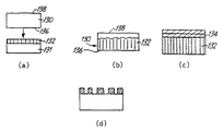
【解決手段】めっきされる基板2に、マスク6および支持体8を含む第1の物品4aを接触させ、第1の金属イオン源が存在している状態で、第1の金属(例えば犠牲金属)12を堆積し、マスク16および支持体18を含む第2の物品14を基板2に接触させ、第2の金属イオン源が存在している状態で、第2の金属(例えば構成金属)20を堆積し、層を平坦化する。そして、異なるパターンの電気めっき物品4a、4b、14a、14bを用いて上記した方法を繰り返し、多層構造24を生成する。犠牲金属12の全てをエッチングすることによって、エレメント26を得る。
【選択図】図11
Description
[電気めっき物品]
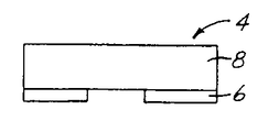
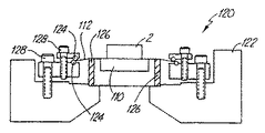
図1を参照して、本発明にかかる電気めっき物品4は、支持体8に付着された、パターン化された適合マスク6を有する。電気めっき物品は、また、パターン化された適合マスクであってもよい。支持体は、ポーラス材(例えばフィルタ)、アノード、およびその結合体であってもよい。物品は、単一の支持体上の複数の異なるマスクパターンを含むことができる。異なるマスクパターンは、連続的に複数の金属層をめっきするために、所定の順序で基板に接触される。各々の金属層は、多層エレメントを形成するために、接触されるマスクパターンに相補的なパターンを有する。図2を参照して、電気めっき物品4は、めっきされる金属を限るために、物品の外表面上の1つ以上のエッジマスク13を含むことができる。
[パターン化された適合マスク]
パターン化された適合マスクは、めっきされる基板の表面に適合するように十分に変形可能(例えば、弾性力をもって変形可能)であり、マスクと基板間の接触を最大にし、マスクと基板間のギャップを最小にする(できれば排除する)。マスクと基板間の接触を最大にすることは、フラッシュ形成のためのポテンシャルを最小にする。マスクは、また、繰り返し使用(すなわち基板と接触し、基板から除去すること)ができるように十分に耐久力のあるものである。マスクは、マスキング圧力によってマスクの形(すなわちマスクパターンのクローズドとオープンの形を構成しているポジティブおよびネガティブの形)の歪みを防ぐように、十分に堅くかつ薄くなっている。マスクは、好ましくは、めっきされる基板のピークと谷の粗さおよび曲率と比較して、相対的に厚くなっている。
[ポーラス材]
ポーラス材は、相互接続された孔を有し、イオンおよび電解液構成物の添加剤に浸透され得る。ポーラス材は、有孔率が変化する1つ以上の層を有することができる。ポーラス材は、好ましくは、マスクの最小のネガティブな形よりかなり細かい小孔寸法を有する。小孔は、好ましくは、開口領域(open area)において一様である。例えば、ポーラス材のいかなる20μm2の開口領域においても、1%である。特に有効なポーラス材は、フィルタとして使われるときに、0.3〜3μmの微少な保有率を有する。複数のポーラス層を含むポーラス材のために、各ポーラス層は、上記の特性を示す、めっきされる基板に最近接のポーラス材でもって、有孔率および小孔寸法が変化し得る。マスクに接触するポーラス材の表面は、めっきされる基板に接触する、付着されたマスク表面も、平らでスムーズであるようにするために、十分に平らでスムーズでなければならない。
[アノード]
電気めっき物品は、アノード上のパターン化されたマスクから構成され得る。アノードは、可溶性もしくは非可溶性であり、堅いもしくはフレキシブルであり、ポーラスかポーラスでないかである。アノードは、腐食しない導電材料(例えば、白金めっきされたチタン)によって支持された腐食可能な層(例えば金属層)を含む。アノードは、金属の薄いフレキシブルな板を含む、任意の大きさのものである。
[電気めっき物品の形成]
一般に、電気めっき物品を形成する方法は、固体のマスクまたは液体のマスキング材を、支持体すなわちアノード、ポーラス材およびその結合体に与えることを含む。固体のマスクは、支持体への取り付けの前、またはそれに続いてパターン化され得る。液体のマスキング材は、ポーラスでない基板(例えば、不活性部材、溶解あるいは溶融(例えば、プラスチックの基板、ラッカーまたは低い融点合金)の上にパターン化され、硬化(cure)され(すなわち、クロスリンクされ、重合され(polymerized)、焼入れされ、固められ、ゲル化され、およびそのコンビネーション)、そして、支持体に取り付けられるかパターン化され、支持体の上で直接固められる。
[支持体の準備]
マスクを受けるスムーズな平らな表面とするために、マスクをうけるであろう支持体の表面を平坦化することが好ましい。マスクをアノードに与えるときに、マスクへの粘着(adhession)を最大にするように、最初にアノードの表面を用意しておくことが好ましい。有効なアノード表面の準備方法の例としては、表面上のパウダーの薄い層を、化学的なマイクロエッチング(microetching)、ラッピング、サンドブラスティング、および焼結(sintering)することを含む。化学薬品の粘着プロモータ(例えば、Sylgard Prime Coat)を使うこともできる。
[電気めっき物品をパターニングし製造すること]
電気めっき物品をパターン化するのに様々な方法を用いることができる。
[電気めっき方法]
本発明は、めっきされる基板を電気めっき物品に接触させることを含む電気めっき方法を特徴とする。その方法は、第1の金属(例えば支持体または犠牲金属(sacrifical metal))に選択的に電気めっきすること、および第2の金属(例えば構成金属(stractural metal))に電気めっきすること、を含む。第2の金属に電気めっきするステップは、本発明の電気めっき物品または第2の金属を一括堆積を用いて、第2の金属に選択的に電気めっきすることを含むことができる。電気めっき方法は、金属の単一の層のめっきに使用する方法、あるいは先に金属層にめっきされて多層構造となっているものの上に付加的に金属をめっきすることを繰り返し行う方法とすることができる。所定層数めっきされた後、少なくとも支持体金属の一部が例えばエッチングによって除去される。残っている構成金属は、微細なあるいはメゾスコピックなデバイスを形成する。
[電気めっき装置]
電気めっき方法は、様々な電気めっき装置において実施することができる。電気めっき方法を実施するための1つの特に有効な装置が、図17に示される。装置56は、2つの槽58、60(例えば、ニッケルめっき漕および銅めっき漕)および検査ステーション62を含む。各槽58、60は、異なる金属に電気めっきをすることができるように構成されている。各槽58、60は、電解液、アノード59、61および電気めっき物品4、14を含む。図示するように、装置56は、めっきされる単一の基板2を収容する。装置は、めっきされる複数のおよび複数の電気めっき物品を収容するように構成することができる。それぞれの物品4、14は、少なくともパターン化されたマスク6、16を含み、金属のパターンを堆積することができる。
[自動化された処理(Automated Processing)]
本発明は、3次元構造のための非常に薄い断面のマスクパターンを生成する方法および3次元構造を形成するための予め定められたシーケンスで生成されたマスクパターンを有する電気めっき物品に接触することを含む自動電気めっきのための方法を特徴とする。
Claims (10)
- 多層3次元構造を製造するための方法において、この方法は、
(i)少なくとも1つの犠牲材料および少なくとも1つの構成材料からなる第1層を基板上に形成し、前記犠牲材料および前記構成材料は平坦化処理によって共通の高さを有しており、
(ii)先に形成された複数の層に隣接し、且つ、接着するように複数の追加の層を形成し、各層は少なくとも1つの犠牲材料および少なくとも1つの構成材料からなり、前記犠牲材料および前記構成材料は平坦化処理によって共通の高さを有しており、
(iii)前記複数の追加の層を形成した後、複数の層において、前記少なくとも1つの構成材料から前記少なくとも1つの犠牲材料をエッチングにより除去することを含み、
前記構造は、前もって整列されたアッセンブルする前の複数の部品を含み、前記少なくとも1つの犠牲材料の少なくとも一部分にエッチングが施された後、前記前もって整列された部品によって形成された通路に沿った相対的な動きによって前記前もって整列された部品が組み立てられる。 - 多層3次元構造を製造するための方法において、この方法は、
(i)少なくとも1つの犠牲材料および少なくとも1つの構成材料からなる第1層を基板上に形成し、前記犠牲材料および前記構成材料は平坦化処理によって共通の高さを有しており、
(ii)先に形成された複数の層に隣接し、且つ、接着するように複数の追加の層を形成し、各層は少なくとも1つの犠牲材料および少なくとも1つの構成材料からなり、前記犠牲材料および前記構成材料は平坦化処理によって共通の高さを有しており、
(iii)前記複数の追加の層を形成した後、複数の層において、前記少なくとも1つの構成材料から前記少なくとも1つの犠牲材料をエッチングにより除去することを含み、
前記構造は、前記複数の層の製造中にアッセンブルされない複数の部品を含み、前記複数の部品の中で少なくとも1つの部品は、アッセンブル後に前記少なくとも1つの部品を他の部品に保持するための1つ以上の保持クリップを含み、前記複数の部品は、前記複数の層の形成後、且つ前記犠牲材料の部分的な除去後に組み立てられる。 - 多層3次元構造を製造するための方法において、この方法は、
(i)少なくとも1つの犠牲材料および少なくとも1つの構成材料からなる第1層を基板上に形成し、前記犠牲材料および前記構成材料は平坦化処理によって共通の高さを有しており、
(ii)先に形成された複数の層に隣接し、且つ、接着するように複数の追加の層を形成し、各層は少なくとも1つの犠牲材料および少なくとも1つの構成材料からなり、前記犠牲材料および前記構成材料は平坦化処理によって共通の高さを有しており、
(iii)前記複数の追加の層を形成した後、複数の層において、前記少なくとも1つの構成材料から前記少なくとも1つの犠牲材料をエッチングにより除去することを含み、
前記複数の層から形成された前記構造は、複数の部品と少なくとも1つの取り付け具を含み、前記取り付け具は、前記複数の追加の層の形成後、且つ前記複数の層から前記少なくとも1つの犠牲材料の少なくとも部分的な除去後に、前記複数の部品をアッセンブルするために用いられる。 - 多層3次元構造を製造するための方法において、この方法は、
(i)少なくとも1つの犠牲材料および少なくとも1つの構成材料からなる第1層を基板上に形成し、前記犠牲材料および前記構成材料は平坦化処理によって共通の高さを有しており、
(ii)先に形成された複数の層に隣接し、且つ、接着するように複数の追加の層を形成し、各層は少なくとも1つの犠牲材料および少なくとも1つの構成材料からなり、前記犠牲材料および前記構成材料は平坦化処理によって共通の高さを有しており、
(iii)前記複数の追加の層を形成した後、複数の層において、前記少なくとも1つの構成材料から前記少なくとも1つの犠牲材料をエッチングにより除去することを含み、
前記複数の追加層の少なくとも一部の形成中に、少なくとも1つの犠牲材料の一部は、少なくとも1つの構成材料もしくは構成材料と前記基板との組み合わせによって十分に保護され、その保護された犠牲材料は、除去されずに前記構造の一部となる。 - 多層3次元構造を製造するための方法において、この方法は、
(i)少なくとも1つの犠牲材料および少なくとも1つの構成材料からなる第1層を基板上に形成し、前記犠牲材料および前記構成材料は平坦化処理によって共通の高さを有しており、
(ii)先に形成された複数の層に隣接し、且つ、接着するように複数の追加の層を形成し、各層は少なくとも1つの犠牲材料および少なくとも1つの構成材料からなり、前記犠牲材料および前記構成材料は平坦化処理によって共通の高さを有しており、
(iii)前記複数の追加の層を形成した後、複数の層において、前記少なくとも1つの構成材料から前記少なくとも1つの犠牲材料をエッチングにより除去することを含み、
前記少なくとも1つの犠牲材料は、選択的に除去可能な少なくとも2つの犠牲材料からなる。 - 多層3次元構造を製造するための方法において、この方法は、
(i)少なくとも1つの犠牲材料および少なくとも1つの構成材料からなる第1層を基板上に形成し、前記犠牲材料および前記構成材料は平坦化処理によって共通の高さを有しており、
(ii)先に形成された複数の層に隣接し、且つ、接着するように複数の追加の層を形成し、各層は少なくとも1つの犠牲材料および少なくとも1つの構成材料からなり、前記犠牲材料および前記構成材料は平坦化処理によって共通の高さを有しており、
(iii)前記複数の追加の層を形成した後、複数の層において、前記少なくとも1つの構成材料から前記少なくとも1つの犠牲材料をエッチングにより除去し、前記構成材料中に多層の空隙を残すようにエッチングバリヤーが形成され、
(iv)前記空隙を異なった構成材料で埋めることを含む。 - 多層3次元構造を製造するための方法において、この方法は、
(i)少なくとも1つの犠牲材料および少なくとも1つの構成材料からなる第1層を基板上に形成し、前記犠牲材料および前記構成材料は平坦化処理によって共通の高さを有しており、
(ii)先に形成された複数の層に隣接し、且つ、接着するように複数の追加の層を形成し、各層は少なくとも1つの犠牲材料および少なくとも1つの構成材料からなり、前記犠牲材料および前記構成材料は平坦化処理によって共通の高さを有しており、
(iii)前記複数の追加の層を形成した後、複数の層において、前記少なくとも1つの構成材料から前記少なくとも1つの犠牲材料をエッチングにより除去することを含み、
前記多層の材料の層の少なくとも一部のそれぞれの形成中に、多数の表面が平坦化される。 - 多層3次元構造を製造するための方法において、この方法は、
(i)少なくとも1つの犠牲材料および少なくとも1つの構成材料からなる第1層を基板上に形成し、前記犠牲材料および前記構成材料は平坦化処理によって共通の高さを有しており、
(ii)先に形成された複数の層に隣接し、且つ、接着するように複数の追加の層を形成し、各層は少なくとも1つの犠牲材料および少なくとも1つの構成材料からなり、前記犠牲材料および前記構成材料は平坦化処理によって共通の高さを有しており、
(iii)前記複数の追加の層を形成した後、複数の層において、前記少なくとも1つの構成材料から前記少なくとも1つの犠牲材料をエッチングにより除去することを含み、
前記多層の材料の少なくとも一部のそれぞれの形成中に、複数のマスクが使用される。 - 多層3次元構造を製造するための方法において、この方法は、
(i)少なくとも1つの犠牲材料および少なくとも1つの構成材料からなる第1層を基板上に形成し、前記犠牲材料および前記構成材料は平坦化処理によって共通の高さを有しており、
(ii)先に形成された複数の層に隣接し、且つ、接着するように複数の追加の層を形成し、各層は少なくとも1つの犠牲材料および少なくとも1つの構成材料からなり、前記犠牲材料および前記構成材料は平坦化処理によって共通の高さを有しており、
(iii)前記複数の追加の層を形成した後、複数の層において、前記少なくとも1つの構成材料から前記少なくとも1つの犠牲材料を超音波振動の存在下でエッチングにより除去することを含む。 - 多層3次元構造を製造するための方法において、この方法は、
(i)少なくとも1つの犠牲材料および少なくとも1つの構成材料からなる第1層を基板上に形成し、前記犠牲材料および前記構成材料は平坦化処理によって共通の高さを有しており、
(ii)先に形成された複数の層に隣接し、且つ、接着するように複数の追加の層を形成し、各層は少なくとも1つの犠牲材料および少なくとも1つの構成材料からなり、前記犠牲材料および前記構成材料は平坦化処理によって共通の高さを有しており、
(iii)前記複数の追加の層を形成した後、複数の層において、前記少なくとも1つの構成材料から前記少なくとも1つの犠牲材料をエッチングにより除去することを含み、前記エッチングを施すエチャントは、前記エチャントを前記少なくとも1つの犠牲材料の方向へ向かわせる複数の噴流によって供給される。
Applications Claiming Priority (1)
| Application Number | Priority Date | Filing Date | Title |
|---|---|---|---|
| US4374297P | 1997-04-04 | 1997-04-04 |
Related Parent Applications (1)
| Application Number | Title | Priority Date | Filing Date |
|---|---|---|---|
| JP2001142210A Division JP2001355095A (ja) | 1997-04-04 | 2001-05-11 | 電気化学製造のための物品、方法、および装置 |
Related Child Applications (1)
| Application Number | Title | Priority Date | Filing Date |
|---|---|---|---|
| JP2011260617A Division JP5449299B2 (ja) | 1997-04-04 | 2011-11-29 | 多層3次元構造を製造するための方法 |
Publications (1)
| Publication Number | Publication Date |
|---|---|
| JP2009102749A true JP2009102749A (ja) | 2009-05-14 |
Family
ID=21928664
Family Applications (8)
| Application Number | Title | Priority Date | Filing Date |
|---|---|---|---|
| JP54291798A Expired - Fee Related JP3269827B2 (ja) | 1997-04-04 | 1998-04-03 | 電気化学製造のための物品、方法、および装置 |
| JP2001142210A Pending JP2001355095A (ja) | 1997-04-04 | 2001-05-11 | 電気化学製造のための物品、方法、および装置 |
| JP2001142211A Pending JP2002011700A (ja) | 1997-04-04 | 2001-05-11 | 電気化学製造のための物品、方法、および装置 |
| JP2009007288A Pending JP2009102743A (ja) | 1997-04-04 | 2009-01-16 | 多層3次元構造を製造するための方法 |
| JP2009029268A Pending JP2009102749A (ja) | 1997-04-04 | 2009-02-12 | 多層3次元構造を製造するための方法 |
| JP2011260617A Expired - Fee Related JP5449299B2 (ja) | 1997-04-04 | 2011-11-29 | 多層3次元構造を製造するための方法 |
| JP2013232987A Expired - Fee Related JP5668124B2 (ja) | 1997-04-04 | 2013-11-11 | 多層3次元構造を製造するための方法 |
| JP2014232626A Expired - Lifetime JP5971312B2 (ja) | 1997-04-04 | 2014-11-17 | 多層3次元構造を製造するための方法 |
Family Applications Before (4)
| Application Number | Title | Priority Date | Filing Date |
|---|---|---|---|
| JP54291798A Expired - Fee Related JP3269827B2 (ja) | 1997-04-04 | 1998-04-03 | 電気化学製造のための物品、方法、および装置 |
| JP2001142210A Pending JP2001355095A (ja) | 1997-04-04 | 2001-05-11 | 電気化学製造のための物品、方法、および装置 |
| JP2001142211A Pending JP2002011700A (ja) | 1997-04-04 | 2001-05-11 | 電気化学製造のための物品、方法、および装置 |
| JP2009007288A Pending JP2009102743A (ja) | 1997-04-04 | 2009-01-16 | 多層3次元構造を製造するための方法 |
Family Applications After (3)
| Application Number | Title | Priority Date | Filing Date |
|---|---|---|---|
| JP2011260617A Expired - Fee Related JP5449299B2 (ja) | 1997-04-04 | 2011-11-29 | 多層3次元構造を製造するための方法 |
| JP2013232987A Expired - Fee Related JP5668124B2 (ja) | 1997-04-04 | 2013-11-11 | 多層3次元構造を製造するための方法 |
| JP2014232626A Expired - Lifetime JP5971312B2 (ja) | 1997-04-04 | 2014-11-17 | 多層3次元構造を製造するための方法 |
Country Status (10)
| Country | Link |
|---|---|
| US (21) | US6027630A (ja) |
| EP (1) | EP1015669B1 (ja) |
| JP (8) | JP3269827B2 (ja) |
| KR (1) | KR100397227B1 (ja) |
| AT (1) | ATE488621T1 (ja) |
| AU (1) | AU743394B2 (ja) |
| CA (4) | CA2572786A1 (ja) |
| DE (1) | DE69842001D1 (ja) |
| IL (1) | IL132165A (ja) |
| WO (1) | WO1998045504A1 (ja) |
Families Citing this family (358)
| Publication number | Priority date | Publication date | Assignee | Title |
|---|---|---|---|---|
| US5599638A (en) * | 1993-10-12 | 1997-02-04 | California Institute Of Technology | Aqueous liquid feed organic fuel cell using solid polymer electrolyte membrane |
| US6703150B2 (en) * | 1993-10-12 | 2004-03-09 | California Institute Of Technology | Direct methanol feed fuel cell and system |
| JP3269827B2 (ja) * | 1997-04-04 | 2002-04-02 | ユニバーシティ・オブ・サザン・カリフォルニア | 電気化学製造のための物品、方法、および装置 |
| JP3780700B2 (ja) * | 1998-05-26 | 2006-05-31 | セイコーエプソン株式会社 | パターン形成方法、パターン形成装置、パターン形成用版、パターン形成用版の製造方法、カラーフィルタの製造方法、導電膜の製造方法及び液晶パネルの製造方法 |
| US6258220B1 (en) | 1998-11-30 | 2001-07-10 | Applied Materials, Inc. | Electro-chemical deposition system |
| US6555408B1 (en) * | 1999-02-05 | 2003-04-29 | Alien Technology Corporation | Methods for transferring elements from a template to a substrate |
| US6436265B1 (en) * | 1999-03-29 | 2002-08-20 | Canon Kabushiki Kaisha | Microstructure array, and apparatus and method for forming the microstructure array, and a mold for fabricating a microstructure array |
| TW408417B (en) * | 1999-05-03 | 2000-10-11 | Ind Tech Res Inst | Planar-shape thin probe having electrostatic actuator manufactured by using sacrificed layer technology and its manufacturing method |
| JP2000331975A (ja) * | 1999-05-19 | 2000-11-30 | Ebara Corp | ウエハ洗浄装置 |
| IT1311361B1 (it) * | 1999-11-15 | 2002-03-12 | Olivetti Lexikon Spa | Testina di stampa monilitica con rete equipotenziale integrata erelativo metodo di fabbricazione. |
| US6294398B1 (en) * | 1999-11-23 | 2001-09-25 | The Trustees Of Princeton University | Method for patterning devices |
| US6299741B1 (en) | 1999-11-29 | 2001-10-09 | Applied Materials, Inc. | Advanced electrolytic polish (AEP) assisted metal wafer planarization method and apparatus |
| US6379223B1 (en) | 1999-11-29 | 2002-04-30 | Applied Materials, Inc. | Method and apparatus for electrochemical-mechanical planarization |
| US6454916B1 (en) * | 2000-01-05 | 2002-09-24 | Advanced Micro Devices, Inc. | Selective electroplating with direct contact chemical polishing |
| US6352935B1 (en) * | 2000-01-18 | 2002-03-05 | Analog Devices, Inc. | Method of forming a cover cap for semiconductor wafer devices |
| AU2001280434A1 (en) * | 2000-05-12 | 2001-11-20 | University Of Southern California | Reflector for laser interrogation of three-dimensional objects |
| US6780353B2 (en) * | 2000-09-26 | 2004-08-24 | Romain L. Billiet | Method for making micromolds |
| US7511675B2 (en) * | 2000-10-26 | 2009-03-31 | Advanced Automotive Antennas, S.L. | Antenna system for a motor vehicle |
| US6422528B1 (en) * | 2001-01-17 | 2002-07-23 | Sandia National Laboratories | Sacrificial plastic mold with electroplatable base |
| GB0102896D0 (en) * | 2001-02-06 | 2001-03-21 | Univ Greenwich | Improved electrophoretic deposition |
| US6762124B2 (en) | 2001-02-14 | 2004-07-13 | Avery Dennison Corporation | Method for patterning a multilayered conductor/substrate structure |
| US20020110673A1 (en) * | 2001-02-14 | 2002-08-15 | Ramin Heydarpour | Multilayered electrode/substrate structures and display devices incorporating the same |
| US6864589B2 (en) * | 2001-03-30 | 2005-03-08 | Sharp Laboratories Of America, Inc. | X/Y alignment vernier formed on a substrate |
| US20040222304A1 (en) * | 2001-04-11 | 2004-11-11 | Matthew Adams | Method and apparatus for on-demand marking or etching of metal |
| US6895667B2 (en) * | 2001-04-13 | 2005-05-24 | The Trustees Of Princeton University | Transfer of patterned metal by cold-welding |
| SE523309E (sv) * | 2001-06-15 | 2010-03-02 | Replisaurus Technologies Ab | Metod, elektrod och apparat för att skapa mikro- och nanostrukturer i ledande material genom mönstring med masterelektrod och elektrolyt |
| US7240420B1 (en) * | 2001-06-19 | 2007-07-10 | Zyvex Labs, Llc | System and method for post-fabrication reduction of minimum feature size spacing of microcomponents |
| US7070687B2 (en) * | 2001-08-14 | 2006-07-04 | Intel Corporation | Apparatus and method of surface treatment for electrolytic and electroless plating of metals in integrated circuit manufacturing |
| US20030071016A1 (en) * | 2001-10-11 | 2003-04-17 | Wu-Sheng Shih | Patterned structure reproduction using nonsticking mold |
| TWI227285B (en) * | 2001-10-15 | 2005-02-01 | Univ Southern California | Methods of and apparatus for producing a three-dimensional structure |
| US6815354B2 (en) * | 2001-10-27 | 2004-11-09 | Nutool, Inc. | Method and structure for thru-mask contact electrodeposition |
| US20040026366A1 (en) * | 2001-11-28 | 2004-02-12 | Andre Sharon | Method of manufacturing ultra-precise, self-assembled micro systems |
| US8382423B1 (en) | 2001-12-03 | 2013-02-26 | Microfabrica Inc. | Micro-scale and meso-scale hydraulically or pneumatically powered devices capable of rotational motion |
| US7501328B2 (en) * | 2003-05-07 | 2009-03-10 | Microfabrica Inc. | Methods for electrochemically fabricating structures using adhered masks, incorporating dielectric sheets, and/or seed layers that are partially removed via planarization |
| US20060282065A1 (en) * | 2002-10-29 | 2006-12-14 | Microfabrica, Inc. | Microtools and methods for fabricating such tools |
| US20070198038A1 (en) * | 2001-12-03 | 2007-08-23 | Cohen Adam L | Microdevices for Tissue Approximation and Retention, Methods for Using, and Methods for Making |
| US20070158200A1 (en) * | 2002-10-29 | 2007-07-12 | Microfabrica Inc. | Electrochemical fabrication processes incorporating non-platable metals and/or metals that are difficult to plate on |
| US20050194348A1 (en) * | 2001-12-03 | 2005-09-08 | University Of Southern California | Electrochemical fabrication methods incorporating dielectric materials and/or using dielectric substrates |
| US20070112338A1 (en) * | 2005-11-01 | 2007-05-17 | Microfabrica Inc. | Microdevices for tissue approximation and retention, methods for using, and methods for making |
| AU2002360464A1 (en) | 2001-12-03 | 2003-06-17 | Memgen Corporation | Miniature rf and microwave components and methods for fabricating such components |
| US20050230261A1 (en) * | 2003-06-27 | 2005-10-20 | Cohen Adam L | Electrochemical fabrication methods incorporating dielectric materials and/or using dielectric substrates |
| US7498714B2 (en) * | 2003-09-24 | 2009-03-03 | Microfabrica Inc. | Multi-layer three-dimensional structures having features smaller than a minimum feature size associated with the formation of individual layers |
| US7686770B2 (en) | 2005-10-14 | 2010-03-30 | Microfabrica Inc. | Discrete or continuous tissue capture device and method for making |
| US20050072681A1 (en) * | 2001-12-03 | 2005-04-07 | Microfabrica Inc. | Multi-step release method for electrochemically fabricated structures |
| US7239219B2 (en) * | 2001-12-03 | 2007-07-03 | Microfabrica Inc. | Miniature RF and microwave components and methods for fabricating such components |
| US7252861B2 (en) | 2002-05-07 | 2007-08-07 | Microfabrica Inc. | Methods of and apparatus for electrochemically fabricating structures via interlaced layers or via selective etching and filling of voids |
| US20080105646A1 (en) * | 2002-05-07 | 2008-05-08 | Microfabrica Inc. | Multi-step Release Method for Electrochemically Fabricated Structures |
| US20050202667A1 (en) * | 2001-12-03 | 2005-09-15 | University Of Southern California | Electrochemical fabrication methods incorporating dielectric materials and/or using dielectric substrates |
| US20080121343A1 (en) * | 2003-12-31 | 2008-05-29 | Microfabrica Inc. | Electrochemical Fabrication Methods Incorporating Dielectric Materials and/or Using Dielectric Substrates |
| US7517462B2 (en) * | 2003-06-27 | 2009-04-14 | Microfabrica Inc. | Electrochemical fabrication methods incorporating dielectric materials and/or using dielectric substrates |
| US20050121411A1 (en) * | 2002-10-29 | 2005-06-09 | Microfabrica Inc. | Medical devices and EFAB methods and apparatus for producing them |
| US20040146650A1 (en) * | 2002-10-29 | 2004-07-29 | Microfabrica Inc. | EFAB methods and apparatus including spray metal or powder coating processes |
| US7674361B2 (en) * | 2003-09-24 | 2010-03-09 | Microfabrica Inc. | Micro-turbines, roller bearings, bushings, and design of hollow closed structures and fabrication methods for creating such structures |
| US9614266B2 (en) | 2001-12-03 | 2017-04-04 | Microfabrica Inc. | Miniature RF and microwave components and methods for fabricating such components |
| WO2003050852A2 (en) * | 2001-12-06 | 2003-06-19 | Memgem Corporation | Complex microdevices and appparatus and methods for fabricating such devices |
| US7185542B2 (en) * | 2001-12-06 | 2007-03-06 | Microfabrica Inc. | Complex microdevices and apparatus and methods for fabricating such devices |
| EP1518822A3 (en) * | 2001-12-06 | 2007-02-28 | Microfabrica Inc. | Complex microdevices and apparatus and methods for fabricating such devices |
| US7372616B2 (en) * | 2001-12-06 | 2008-05-13 | Microfabrica, Inc. | Complex microdevices and apparatus and methods for fabricating such devices |
| JP2003260142A (ja) * | 2002-03-11 | 2003-09-16 | Kanegafuchi Chem Ind Co Ltd | 頭蓋内血管治療用ステント及び製造方法 |
| US20030221968A1 (en) * | 2002-03-13 | 2003-12-04 | Memgen Corporation | Electrochemical fabrication method and apparatus for producing three-dimensional structures having improved surface finish |
| US20030201170A1 (en) * | 2002-04-24 | 2003-10-30 | Applied Materials, Inc. | Apparatus and method for electropolishing a substrate in an electroplating cell |
| US20030201185A1 (en) * | 2002-04-29 | 2003-10-30 | Applied Materials, Inc. | In-situ pre-clean for electroplating process |
| US20060006888A1 (en) * | 2003-02-04 | 2006-01-12 | Microfabrica Inc. | Electrochemically fabricated microprobes |
| AU2003228973A1 (en) * | 2002-05-07 | 2003-11-11 | Memgen Corporation | Electrochemically fabricated hermetically sealed microstructures |
| US7531077B2 (en) | 2003-02-04 | 2009-05-12 | Microfabrica Inc. | Electrochemical fabrication process for forming multilayer multimaterial microprobe structures |
| US20070045121A1 (en) * | 2002-05-07 | 2007-03-01 | Microfabrica Inc. | Electrochemically fabricated hermetically sealed microstructures and methods of and apparatus for producing such structures |
| US20050202660A1 (en) * | 2002-05-07 | 2005-09-15 | Microfabrica Inc. | Electrochemical fabrication process including process monitoring, making corrective action decisions, and taking appropriate actions |
| US20060051948A1 (en) * | 2003-02-04 | 2006-03-09 | Microfabrica Inc. | Microprobe tips and methods for making |
| US7265565B2 (en) | 2003-02-04 | 2007-09-04 | Microfabrica Inc. | Cantilever microprobes for contacting electronic components and methods for making such probes |
| US7611616B2 (en) * | 2002-05-07 | 2009-11-03 | Microfabrica Inc. | Mesoscale and microscale device fabrication methods using split structures and alignment elements |
| US7640651B2 (en) * | 2003-12-31 | 2010-01-05 | Microfabrica Inc. | Fabrication process for co-fabricating multilayer probe array and a space transformer |
| US20060238209A1 (en) * | 2002-05-07 | 2006-10-26 | Microfabrica Inc. | Vertical microprobes for contacting electronic components and method for making such probes |
| US20060053625A1 (en) * | 2002-05-07 | 2006-03-16 | Microfabrica Inc. | Microprobe tips and methods for making |
| US7384530B2 (en) * | 2002-05-07 | 2008-06-10 | Microfabrica Inc. | Methods for electrochemically fabricating multi-layer structures including regions incorporating maskless, patterned, multiple layer thickness depositions of selected materials |
| AU2003228977A1 (en) * | 2002-05-07 | 2003-11-11 | University Of Southern California | Method of and apparatus for forming three-dimensional structures integral with semiconductor based circuitry |
| EP1576207A2 (en) * | 2002-05-07 | 2005-09-21 | Microfabrica Inc. | Methods of and apparatus for molding structures |
| US8070931B1 (en) | 2002-05-07 | 2011-12-06 | Microfabrica Inc. | Electrochemical fabrication method including elastic joining of structures |
| US20050184748A1 (en) * | 2003-02-04 | 2005-08-25 | Microfabrica Inc. | Pin-type probes for contacting electronic circuits and methods for making such probes |
| US9919472B1 (en) | 2002-05-07 | 2018-03-20 | Microfabrica Inc. | Stacking and bonding methods for forming multi-layer, three-dimensional, millimeter scale and microscale structures |
| US20040065550A1 (en) * | 2002-05-07 | 2004-04-08 | University Of Southern California | Electrochemical fabrication methods with enhanced post deposition processing |
| AU2003228974A1 (en) * | 2002-05-07 | 2003-11-11 | Memgen Corporation | Method of and apparatus for forming three-dimensional structures |
| US7273812B2 (en) * | 2002-05-07 | 2007-09-25 | Microfabrica Inc. | Microprobe tips and methods for making |
| US7363705B2 (en) * | 2003-02-04 | 2008-04-29 | Microfabrica, Inc. | Method of making a contact |
| AU2003234398A1 (en) * | 2002-05-07 | 2003-11-11 | Memgen Corporation | Electrochemically fabricated structures having dielectric or active bases |
| US20040065551A1 (en) * | 2002-05-07 | 2004-04-08 | University Of Southern California | Electrochemical deposition with enhanced uniform deposition capabilities and/or enhanced longevity of contact masks |
| US20050104609A1 (en) * | 2003-02-04 | 2005-05-19 | Microfabrica Inc. | Microprobe tips and methods for making |
| US20060108678A1 (en) | 2002-05-07 | 2006-05-25 | Microfabrica Inc. | Probe arrays and method for making |
| US20050045585A1 (en) * | 2002-05-07 | 2005-03-03 | Gang Zhang | Method of electrochemically fabricating multilayer structures having improved interlayer adhesion |
| US20040007469A1 (en) * | 2002-05-07 | 2004-01-15 | Memgen Corporation | Selective electrochemical deposition methods using pyrophosphate copper plating baths containing ammonium salts, citrate salts and/or selenium oxide |
| US20050029109A1 (en) * | 2002-05-07 | 2005-02-10 | Gang Zhang | Method of electrochemically fabricating multilayer structures having improved interlayer adhesion |
| US20040000489A1 (en) * | 2002-05-07 | 2004-01-01 | University Of Southern California | Methods and apparatus for monitoring deposition quality during conformable contact mask plating operations |
| US20050029225A1 (en) * | 2002-05-07 | 2005-02-10 | University Of Southern California | Electrochemical fabrication methods with enhanced post deposition processing |
| US20050067292A1 (en) * | 2002-05-07 | 2005-03-31 | Microfabrica Inc. | Electrochemically fabricated structures having dielectric or active bases and methods of and apparatus for producing such structures |
| US7412767B2 (en) * | 2003-02-04 | 2008-08-19 | Microfabrica, Inc. | Microprobe tips and methods for making |
| US20050142739A1 (en) * | 2002-05-07 | 2005-06-30 | Microfabrica Inc. | Probe arrays and method for making |
| AU2003229023A1 (en) * | 2002-05-07 | 2003-11-11 | University Of Southern California | Conformable contact masking methods and apparatus utilizing in situ cathodic activation of a substrate |
| US20080050524A1 (en) * | 2006-04-07 | 2008-02-28 | Microfabrica Inc. | Methods of Forming Three-Dimensional Structures Having Reduced Stress and/or Curvature |
| CN100567581C (zh) * | 2002-05-07 | 2009-12-09 | 微制造公司 | 电化学制造结构的多步释放方法 |
| WO2003096123A1 (en) * | 2002-05-08 | 2003-11-20 | Agency For Science, Technology And Research | Reversal imprint technique |
| US20030209523A1 (en) * | 2002-05-09 | 2003-11-13 | Applied Materials, Inc. | Planarization by chemical polishing for ULSI applications |
| US7189313B2 (en) * | 2002-05-09 | 2007-03-13 | Applied Materials, Inc. | Substrate support with fluid retention band |
| JP2005532015A (ja) * | 2002-06-27 | 2005-10-20 | マイクロファブリカ インク | 小型のrfおよびマイクロ波の構成要素とそのような構成要素を製造するための方法 |
| US20040072445A1 (en) * | 2002-07-11 | 2004-04-15 | Applied Materials, Inc. | Effective method to improve surface finish in electrochemically assisted CMP |
| US20040118694A1 (en) * | 2002-12-19 | 2004-06-24 | Applied Materials, Inc. | Multi-chemistry electrochemical processing system |
| WO2004032210A2 (en) * | 2002-10-01 | 2004-04-15 | Microfabrica Inc. | Monolithic structures including alignment and/or retention fixtures for accepting components |
| US7235166B2 (en) * | 2002-10-01 | 2007-06-26 | Microfabrica Inc. | Multi-cell masks and methods and apparatus for using such masks to form three-dimensional structures |
| US7229544B2 (en) * | 2002-10-01 | 2007-06-12 | University Of Southern California | Multi-cell masks and methods and apparatus for using such masks to form three-dimensional structures |
| US20050167894A1 (en) * | 2002-10-08 | 2005-08-04 | Wu-Sheng Shih | Patterned structure reproduction using nonsticking mold |
| US20100094320A1 (en) * | 2002-10-29 | 2010-04-15 | Microfabrica Inc. | Atherectomy and Thrombectomy Devices, Methods for Making, and Procedures for Using |
| US8454652B1 (en) | 2002-10-29 | 2013-06-04 | Adam L. Cohen | Releasable tissue anchoring device, methods for using, and methods for making |
| US20110092988A1 (en) * | 2002-10-29 | 2011-04-21 | Microfabrica Inc. | Microdevices for Tissue Approximation and Retention, Methods for Using, and Methods for Making |
| US7368044B2 (en) * | 2002-11-26 | 2008-05-06 | Microfabrica, Inc. | Non-conformable masks and methods and apparatus for forming three-dimensional structures |
| US7291254B2 (en) * | 2002-11-26 | 2007-11-06 | Microfabrica, Inc. | Method for electrochemically forming structures including non-parallel mating of contact masks and substrates |
| JP2006517055A (ja) * | 2002-12-09 | 2006-07-13 | エーシーエム リサーチ,インコーポレイティド | ウェファチャックと研磨/鍍金の容器との整列の測定 |
| US6916409B1 (en) | 2002-12-31 | 2005-07-12 | Advanced Cardiovascular Systems, Inc. | Apparatus and process for electrolytic removal of material from a medical device |
| US6875322B1 (en) | 2003-01-15 | 2005-04-05 | Lam Research Corporation | Electrochemical assisted CMP |
| US20040239006A1 (en) * | 2003-01-22 | 2004-12-02 | Microfabrica Inc. | Silicone compositions, methods of making, and uses thereof |
| US7567089B2 (en) * | 2003-02-04 | 2009-07-28 | Microfabrica Inc. | Two-part microprobes for contacting electronic components and methods for making such probes |
| US10416192B2 (en) | 2003-02-04 | 2019-09-17 | Microfabrica Inc. | Cantilever microprobes for contacting electronic components |
| US9244101B2 (en) * | 2003-02-04 | 2016-01-26 | University Of Southern California | Electrochemical fabrication process for forming multilayer multimaterial microprobe structures |
| US8613846B2 (en) * | 2003-02-04 | 2013-12-24 | Microfabrica Inc. | Multi-layer, multi-material fabrication methods for producing micro-scale and millimeter-scale devices with enhanced electrical and/or mechanical properties |
| US20080211524A1 (en) * | 2003-02-04 | 2008-09-04 | Microfabrica Inc. | Electrochemically Fabricated Microprobes |
| US20060226015A1 (en) * | 2003-02-04 | 2006-10-12 | Microfabrica Inc. | Method of forming electrically isolated structures using thin dielectric coatings |
| US20080106280A1 (en) * | 2003-02-04 | 2008-05-08 | Microfabrica Inc. | Vertical Microprobes for Contacting Electronic Components and Method for Making Such Probes |
| WO2004079795A2 (en) * | 2003-03-04 | 2004-09-16 | Rohm And Haas Electronic Materials, L.L.C. | Coaxial waveguide microstructures and methods of formation thereof |
| JP3898137B2 (ja) * | 2003-03-06 | 2007-03-28 | 富士通株式会社 | 自動出力復帰方法および光通信システム |
| US7198704B2 (en) * | 2003-04-21 | 2007-04-03 | Microfabrica Inc. | Methods of reducing interlayer discontinuities in electrochemically fabricated three-dimensional structures |
| US7433811B2 (en) * | 2003-05-06 | 2008-10-07 | The Regents Of The University Of California | Direct patterning of silicon by photoelectrochemical etching |
| US10297421B1 (en) * | 2003-05-07 | 2019-05-21 | Microfabrica Inc. | Plasma etching of dielectric sacrificial material from reentrant multi-layer metal structures |
| US9671429B2 (en) | 2003-05-07 | 2017-06-06 | University Of Southern California | Multi-layer, multi-material micro-scale and millimeter-scale devices with enhanced electrical and/or mechanical properties |
| WO2004101856A2 (en) * | 2003-05-07 | 2004-11-25 | Microfabrica Inc. | Methods for electrochemically fabricating structures using adhered masks, incorporating dielectric sheets, and/or seed layers that are partially removed via planarization |
| TWI232843B (en) * | 2003-05-07 | 2005-05-21 | Microfabrica Inc | Electrochemical fabrication methods including use of surface treatments to reduce overplating and/or planarization during formation of multi-layer three-dimensional structures |
| TWI291500B (en) * | 2003-05-07 | 2007-12-21 | Univ Southern California | Method of electrochemically fabricating multilayer structures having improved interlayer adhesion |
| WO2004101857A2 (en) * | 2003-05-07 | 2004-11-25 | Microfabrica Inc. | Methods and apparatus for forming multi-layer structures using adhered masks |
| US7527721B2 (en) * | 2003-05-07 | 2009-05-05 | Microfabrica Inc. | Electrochemical fabrication method for producing multi-layer three-dimensional structures on a porous dielectric |
| US7244326B2 (en) * | 2003-05-16 | 2007-07-17 | Alien Technology Corporation | Transfer assembly for manufacturing electronic devices |
| US7131578B2 (en) | 2003-05-28 | 2006-11-07 | Ewi Holdings, Inc. | System and method for electronic prepaid account replenishment |
| US7465661B2 (en) * | 2003-05-28 | 2008-12-16 | The United States Of America As Represented By The Secretary Of The Navy | High aspect ratio microelectrode arrays |
| US20050194258A1 (en) * | 2003-06-27 | 2005-09-08 | Microfabrica Inc. | Electrochemical fabrication methods incorporating dielectric materials and/or using dielectric substrates |
| US20050176238A1 (en) * | 2003-06-27 | 2005-08-11 | Microfabrica Inc. | Electrochemical fabrication methods incorporating dielectric materials and/or using dielectric substrates |
| US20050215046A1 (en) * | 2003-06-27 | 2005-09-29 | Cohen Adam L | Electrochemical fabrication methods incorporating dielectric materials and/or using dielectric substrates |
| US7524427B2 (en) * | 2003-06-27 | 2009-04-28 | Microfabrica Inc. | Electrochemical fabrication methods incorporating dielectric materials and/or using dielectric substrates |
| US20050053849A1 (en) * | 2003-07-03 | 2005-03-10 | Microfabrica Inc. | Electrochemical fabrication method for producing compliant beam-like structures |
| KR101105991B1 (ko) | 2003-07-09 | 2012-01-18 | 프라이즈 메탈즈, 인크. | 침착 및 패턴 공정 |
| US20190357827A1 (en) | 2003-08-01 | 2019-11-28 | Dexcom, Inc. | Analyte sensor |
| CN1997691B (zh) * | 2003-09-23 | 2011-07-20 | 北卡罗来纳大学查珀尔希尔分校 | 光固化的全氟聚醚用作微流体器件中的新材料 |
| US20050145122A1 (en) * | 2003-09-24 | 2005-07-07 | Matthew Adams | Use of a UV-curable thermal ribbon in conjunction with a porous substrate to form a durable, on-demand electro-chemical stencil |
| US20050067286A1 (en) * | 2003-09-26 | 2005-03-31 | The University Of Cincinnati | Microfabricated structures and processes for manufacturing same |
| WO2005033798A2 (en) * | 2003-10-03 | 2005-04-14 | University Of Washington | Electrochemical micromanufacturing system and method |
| US20050205430A1 (en) * | 2003-11-26 | 2005-09-22 | Microfabrica Inc. | EFAB methods including controlled mask to substrate mating |
| EP1538482B1 (en) * | 2003-12-05 | 2016-02-17 | Obducat AB | Device and method for large area lithography |
| US8532730B2 (en) | 2006-10-04 | 2013-09-10 | Dexcom, Inc. | Analyte sensor |
| US20060127581A1 (en) * | 2003-12-11 | 2006-06-15 | Aspens Glenn D | Method for on-demand direct item marking via a screen printing process |
| US8521284B2 (en) | 2003-12-12 | 2013-08-27 | Cardiac Pacemakers, Inc. | Cardiac response classification using multisite sensing and pacing |
| US9040090B2 (en) * | 2003-12-19 | 2015-05-26 | The University Of North Carolina At Chapel Hill | Isolated and fixed micro and nano structures and methods thereof |
| DK1704585T3 (en) | 2003-12-19 | 2017-05-22 | Univ North Carolina Chapel Hill | Methods for preparing isolated micro- and nanostructures using soft lithography or printing lithography |
| US7479213B2 (en) * | 2003-12-25 | 2009-01-20 | Ebara Corporation | Plating method and plating apparatus |
| US7623935B2 (en) * | 2003-12-31 | 2009-11-24 | University Of Southern California | Method for electrochemically fabricating three-dimensional structures including pseudo-rasterization of data |
| US20080142369A1 (en) * | 2003-12-31 | 2008-06-19 | Microfabrica Inc. | Integrated Circuit Packaging Using Electrochemically Fabricated Structures |
| US10641792B2 (en) | 2003-12-31 | 2020-05-05 | University Of Southern California | Multi-layer, multi-material micro-scale and millimeter-scale devices with enhanced electrical and/or mechanical properties |
| US20080108221A1 (en) * | 2003-12-31 | 2008-05-08 | Microfabrica Inc. | Microprobe Tips and Methods for Making |
| US20090020433A1 (en) * | 2003-12-31 | 2009-01-22 | Microfabrica Inc. | Electrochemical Fabrication Methods for Producing Multilayer Structures Including the use of Diamond Machining in the Planarization of Deposits of Material |
| US20060134831A1 (en) * | 2003-12-31 | 2006-06-22 | Microfabrica Inc. | Integrated circuit packaging using electrochemically fabricated structures |
| US20160194774A1 (en) * | 2003-12-31 | 2016-07-07 | University Of Southern California | Electrochemical Fabrication Process for Forming Multilayer Multimaterial Microprobe Structures Incorporating Dielectrics |
| US7430731B2 (en) * | 2003-12-31 | 2008-09-30 | University Of Southern California | Method for electrochemically fabricating three-dimensional structures including pseudo-rasterization of data |
| US20080105355A1 (en) * | 2003-12-31 | 2008-05-08 | Microfabrica Inc. | Probe Arrays and Method for Making |
| US20050202180A1 (en) * | 2003-12-31 | 2005-09-15 | Microfabrica Inc. | Electrochemical fabrication methods for producing multilayer structures including the use of diamond machining in the planarization of deposits of material |
| US7833389B1 (en) | 2005-01-21 | 2010-11-16 | Microcontinuum, Inc. | Replication tools and related fabrication methods and apparatus |
| US9307648B2 (en) | 2004-01-21 | 2016-04-05 | Microcontinuum, Inc. | Roll-to-roll patterning of transparent and metallic layers |
| US7674103B2 (en) | 2005-01-21 | 2010-03-09 | Microcontinuum, Inc. | Replication tools and related fabrication methods and apparatus |
| JP2005223063A (ja) * | 2004-02-04 | 2005-08-18 | Seiko Epson Corp | 配線基板の製造方法及び電子デバイスの製造方法 |
| CN101189271A (zh) * | 2004-02-13 | 2008-05-28 | 北卡罗来纳大学查珀尔希尔分校 | 制造微流体设备的功能材料和新型方法 |
| US7280644B2 (en) | 2004-12-07 | 2007-10-09 | Ewi Holdings, Inc. | Transaction processing platform for faciliating electronic distribution of plural prepaid services |
| US7256107B2 (en) * | 2004-05-04 | 2007-08-14 | The Regents Of The University Of California | Damascene process for use in fabricating semiconductor structures having micro/nano gaps |
| EP1594001B1 (en) * | 2004-05-07 | 2015-12-30 | Obducat AB | Device and method for imprint lithography |
| US8988091B2 (en) * | 2004-05-21 | 2015-03-24 | Microprobe, Inc. | Multiple contact probes |
| US9097740B2 (en) * | 2004-05-21 | 2015-08-04 | Formfactor, Inc. | Layered probes with core |
| US7659739B2 (en) * | 2006-09-14 | 2010-02-09 | Micro Porbe, Inc. | Knee probe having reduced thickness section for control of scrub motion |
| US7759949B2 (en) * | 2004-05-21 | 2010-07-20 | Microprobe, Inc. | Probes with self-cleaning blunt skates for contacting conductive pads |
| US7733101B2 (en) * | 2004-05-21 | 2010-06-08 | Microprobe, Inc. | Knee probe having increased scrub motion |
| USRE43503E1 (en) | 2006-06-29 | 2012-07-10 | Microprobe, Inc. | Probe skates for electrical testing of convex pad topologies |
| US9476911B2 (en) | 2004-05-21 | 2016-10-25 | Microprobe, Inc. | Probes with high current carrying capability and laser machining methods |
| GB0416600D0 (en) * | 2004-07-24 | 2004-08-25 | Univ Newcastle | A process for manufacturing micro- and nano-devices |
| US6956389B1 (en) * | 2004-08-16 | 2005-10-18 | Jem America Corporation | Highly resilient cantilever spring probe for testing ICs |
| WO2006023696A2 (en) * | 2004-08-19 | 2006-03-02 | Microfabrica, Inc. | Integrated circuit packaging using electrochemically fabricated |
| US7169649B2 (en) * | 2004-12-16 | 2007-01-30 | Palo Alto Research Center, Inc. | Wafer scale integration of electroplated 3D structures using successive lithography, electroplated sacrificial layers, and flip-chip bonding |
| US7335463B2 (en) * | 2004-12-16 | 2008-02-26 | Palo Alto Research Center, Inc. | Electroplated three dimensional ink jet manifold and nozzle structures using successive lithography and electroplated sacrificial layers |
| KR20070119624A (ko) * | 2005-02-03 | 2007-12-20 | 유니버시티 오브 노스캐롤라이나 앳 채플 힐 | 액정 디스플레이에서 사용되는 낮은 표면 에너지 고분자물질 |
| JP4479535B2 (ja) * | 2005-02-21 | 2010-06-09 | セイコーエプソン株式会社 | 光学素子の製造方法 |
| US7696102B2 (en) * | 2005-03-31 | 2010-04-13 | Gang Zhang | Methods for fabrication of three-dimensional structures |
| US8216931B2 (en) * | 2005-03-31 | 2012-07-10 | Gang Zhang | Methods for forming multi-layer three-dimensional structures |
| JP4624873B2 (ja) * | 2005-06-28 | 2011-02-02 | 株式会社荏原製作所 | めっき方法 |
| US7419630B2 (en) * | 2005-04-22 | 2008-09-02 | Sandia Corporation | Methods and systems for rapid prototyping of high density circuits |
| WO2006125089A2 (en) * | 2005-05-18 | 2006-11-23 | Fry's Metals, Inc. | Mask and method for electrokinetic deposition and patterning process on substrates |
| FR2885913B1 (fr) * | 2005-05-18 | 2007-08-10 | Centre Nat Rech Scient | Element composite comprenant un substrat conducteur et un revetement metallique nanostructure. |
| KR101137862B1 (ko) * | 2005-06-17 | 2012-04-20 | 엘지디스플레이 주식회사 | 평판표시소자의 제조방법 |
| EP1905065B1 (en) * | 2005-06-20 | 2014-08-13 | Microcontinuum, Inc. | Roll-to-roll patterning |
| US8273117B2 (en) * | 2005-06-22 | 2012-09-25 | Integran Technologies Inc. | Low texture, quasi-isotropic metallic stent |
| US20090304992A1 (en) * | 2005-08-08 | 2009-12-10 | Desimone Joseph M | Micro and Nano-Structure Metrology |
| EP1922364A4 (en) | 2005-08-09 | 2010-04-21 | Univ North Carolina | METHOD AND MATERIALS FOR PRODUCING MICROFLUIDIC DEVICES |
| WO2007022267A2 (en) * | 2005-08-15 | 2007-02-22 | University Of Florida Research Foundation, Inc. | Micro-molded integral non-line-of sight articles and method |
| US7767126B2 (en) * | 2005-08-22 | 2010-08-03 | Sipix Imaging, Inc. | Embossing assembly and methods of preparation |
| CN101305454B (zh) * | 2005-11-07 | 2010-05-19 | 应用材料股份有限公司 | 形成光致电压接点和连线的方法 |
| US20090234417A1 (en) * | 2005-11-10 | 2009-09-17 | Electrocore, Inc. | Methods And Apparatus For The Treatment Of Metabolic Disorders |
| WO2007058605A1 (en) * | 2005-11-18 | 2007-05-24 | Replisaurus Technologies Ab | Master electrode and method of forming it |
| US7649367B2 (en) * | 2005-12-07 | 2010-01-19 | Microprobe, Inc. | Low profile probe having improved mechanical scrub and reduced contact inductance |
| US7658831B2 (en) * | 2005-12-21 | 2010-02-09 | Formfactor, Inc | Three dimensional microstructures and methods for making three dimensional microstructures |
| IL173121A (en) * | 2006-01-12 | 2011-07-31 | Dina Katsir | Electrodes, membranes, printing plate precursors and other articles including multi-strata porous coatings |
| EP1987358A4 (en) * | 2006-01-26 | 2013-12-04 | California Inst Of Techn | MECHANICALLY INTRODUCED TRAPPING OF MOLECULAR INTERACTIONS |
| CA2643510C (en) | 2006-02-27 | 2014-04-29 | Microcontinuum, Inc. | Formation of pattern replicating tools |
| EP1835339B1 (fr) * | 2006-03-15 | 2012-05-16 | Rolex S.A. | Procédé de fabrication par technologie de type liga d'une structure métallique monocouche ou multicouche, et structure obtenue |
| US7312617B2 (en) | 2006-03-20 | 2007-12-25 | Microprobe, Inc. | Space transformers employing wire bonds for interconnections with fine pitch contacts |
| US7655126B2 (en) | 2006-03-27 | 2010-02-02 | Federal Mogul World Wide, Inc. | Fabrication of topical stopper on MLS gasket by active matrix electrochemical deposition |
| US7622382B2 (en) * | 2006-03-29 | 2009-11-24 | Intel Corporation | Filling narrow and high aspect ratio openings with electroless deposition |
| US7998323B1 (en) | 2006-06-07 | 2011-08-16 | Actus Potentia, Inc. | Apparatus for focused electric-field imprinting for micron and sub-micron patterns on wavy or planar surfaces |
| WO2008011051A1 (en) * | 2006-07-17 | 2008-01-24 | Liquidia Technologies, Inc. | Nanoparticle fabrication methods, systems, and materials |
| US7876087B2 (en) * | 2006-09-12 | 2011-01-25 | Innoconnex, Inc. | Probe card repair using coupons with spring contacts and separate atachment points |
| US9615463B2 (en) * | 2006-09-22 | 2017-04-04 | Oscar Khaselev | Method for producing a high-aspect ratio conductive pattern on a substrate |
| CN101161870B (zh) * | 2006-10-11 | 2010-11-10 | 富准精密工业(深圳)有限公司 | 气密性腔体成型方法 |
| US8907689B2 (en) | 2006-10-11 | 2014-12-09 | Microprobe, Inc. | Probe retention arrangement |
| US7786740B2 (en) * | 2006-10-11 | 2010-08-31 | Astria Semiconductor Holdings, Inc. | Probe cards employing probes having retaining portions for potting in a potting region |
| US7799182B2 (en) | 2006-12-01 | 2010-09-21 | Applied Materials, Inc. | Electroplating on roll-to-roll flexible solar cell substrates |
| US7736928B2 (en) * | 2006-12-01 | 2010-06-15 | Applied Materials, Inc. | Precision printing electroplating through plating mask on a solar cell substrate |
| US7704352B2 (en) * | 2006-12-01 | 2010-04-27 | Applied Materials, Inc. | High-aspect ratio anode and apparatus for high-speed electroplating on a solar cell substrate |
| US20080127490A1 (en) * | 2006-12-01 | 2008-06-05 | Lotes Co., Ltd. | Manufacture process of connector |
| US20080128019A1 (en) * | 2006-12-01 | 2008-06-05 | Applied Materials, Inc. | Method of metallizing a solar cell substrate |
| KR101253274B1 (ko) * | 2006-12-07 | 2013-04-10 | 삼성디스플레이 주식회사 | 도광판 제조용 금형 제조 방법 및 이를 이용한 도광판 제조방법 |
| US8877074B2 (en) * | 2006-12-15 | 2014-11-04 | The Regents Of The University Of California | Methods of manufacturing microdevices in laminates, lead frames, packages, and printed circuit boards |
| US7763326B2 (en) * | 2006-12-20 | 2010-07-27 | United Technologies Corporation | Photocurable maskant composition and method of use |
| CN101274734A (zh) | 2006-12-30 | 2008-10-01 | 罗门哈斯电子材料有限公司 | 三维微结构及其形成方法 |
| US7898356B2 (en) | 2007-03-20 | 2011-03-01 | Nuvotronics, Llc | Coaxial transmission line microstructures and methods of formation thereof |
| EP3104450A3 (en) | 2007-03-20 | 2016-12-28 | Nuvotronics, LLC | Integrated electronic components and methods of formation thereof |
| US20100151031A1 (en) * | 2007-03-23 | 2010-06-17 | Desimone Joseph M | Discrete size and shape specific organic nanoparticles designed to elicit an immune response |
| US7514948B2 (en) * | 2007-04-10 | 2009-04-07 | Microprobe, Inc. | Vertical probe array arranged to provide space transformation |
| GB0715621D0 (en) * | 2007-08-10 | 2007-09-19 | Rolls Royce Plc | Support architecture |
| US20100121307A1 (en) * | 2007-08-24 | 2010-05-13 | Microfabrica Inc. | Microneedles, Microneedle Arrays, Methods for Making, and Transdermal and/or Intradermal Applications |
| US7918984B2 (en) * | 2007-09-17 | 2011-04-05 | International Business Machines Corporation | Method of electrodepositing germanium compound materials on a substrate |
| US8498464B2 (en) * | 2007-09-27 | 2013-07-30 | Siemens Medical Solutions Usa, Inc. | Intrinsic co-registration for modular multimodality medical imaging systems |
| US8723546B2 (en) * | 2007-10-19 | 2014-05-13 | Microprobe, Inc. | Vertical guided layered probe |
| US7671610B2 (en) * | 2007-10-19 | 2010-03-02 | Microprobe, Inc. | Vertical guided probe array providing sideways scrub motion |
| WO2009054175A1 (ja) * | 2007-10-24 | 2009-04-30 | Honda Motor Co., Ltd. | 板金成型用のプレス金型及びプレス金型表面の処理方法、並びに車体の生産方法 |
| FR2923078B1 (fr) * | 2007-10-26 | 2017-09-01 | Centre Nat De La Rech Scient - Cnrs | Procede de fabrication d'un element d'interconnexion mecanique conducteur d'electricite. |
| JP2009117699A (ja) * | 2007-11-08 | 2009-05-28 | Shinko Electric Ind Co Ltd | 半導体パッケージ用部品及び半導体パッケージ用部品の製造方法 |
| AU2008323666A1 (en) * | 2007-11-09 | 2009-05-14 | Firestar Engineering, Llc | Nitrous oxide fuel blend monopropellants |
| KR101689519B1 (ko) * | 2007-12-26 | 2016-12-26 | 가부시키가이샤 한도오따이 에네루기 켄큐쇼 | 증착용 기판, 증착용 기판의 제조방법, 및 발광장치의 제조방법 |
| JP4913082B2 (ja) * | 2008-03-03 | 2012-04-11 | 株式会社東芝 | 三次元構造体の製造方法および三次元構造体 |
| US8078309B1 (en) * | 2008-03-31 | 2011-12-13 | The United States Of America As Represented By The Administrator Of The National Aeronautics And Space Administration | Method to create arbitrary sidewall geometries in 3-dimensions using liga with a stochastic optimization framework |
| US8230593B2 (en) * | 2008-05-29 | 2012-07-31 | Microprobe, Inc. | Probe bonding method having improved control of bonding material |
| JP2009291293A (ja) | 2008-06-03 | 2009-12-17 | Olympus Corp | 積層構造体、光調節装置、及び積層構造体の製造方法 |
| US9814484B2 (en) | 2012-11-29 | 2017-11-14 | Microfabrica Inc. | Micro debrider devices and methods of tissue removal |
| US10939934B2 (en) | 2008-06-23 | 2021-03-09 | Microfabrica Inc. | Miniature shredding tools for use in medical applications, methods for making, and procedures for using |
| WO2010151251A1 (en) * | 2008-06-23 | 2010-12-29 | Microfabrica Inc. | Miniature shredding tool for use in medical applications and methods for making |
| US9451977B2 (en) | 2008-06-23 | 2016-09-27 | Microfabrica Inc. | MEMS micro debrider devices and methods of tissue removal |
| US8414607B1 (en) | 2008-06-23 | 2013-04-09 | Microfabrica Inc. | Miniature shredding tool for use in medical applications and methods for making |
| US8795278B2 (en) | 2008-06-23 | 2014-08-05 | Microfabrica Inc. | Selective tissue removal tool for use in medical applications and methods for making and using |
| US20100147677A1 (en) * | 2008-10-28 | 2010-06-17 | Mustafa Pinarbasi | Drum design for web processing |
| US9149220B2 (en) | 2011-04-15 | 2015-10-06 | Dexcom, Inc. | Advanced analyte sensor calibration and error detection |
| US20100126849A1 (en) * | 2008-11-24 | 2010-05-27 | Applied Materials, Inc. | Apparatus and method for forming 3d nanostructure electrode for electrochemical battery and capacitor |
| US8511960B1 (en) | 2008-12-31 | 2013-08-20 | Microfabrica Inc. | Microscale and millimeter scale devices including threaded elements, methods for designing, and methods for making |
| US9441661B2 (en) | 2008-12-31 | 2016-09-13 | Microfabrica Inc. | Microscale and millimeter scale devices including threaded elements, methods for designing, and methods for making |
| JP5319326B2 (ja) * | 2009-02-25 | 2013-10-16 | 株式会社東芝 | 凹凸パターンの形成方法および凹凸パターン形成用シート |
| US8073019B2 (en) * | 2009-03-02 | 2011-12-06 | Jian Liu | 810 nm ultra-short pulsed fiber laser |
| US8362578B2 (en) * | 2009-06-02 | 2013-01-29 | Taiwan Semiconductor Manufacturing Company, Ltd. | Triple-axis MEMS accelerometer |
| WO2010151504A1 (en) | 2009-06-24 | 2010-12-29 | Ultradent Products, Inc. | Low force orthodontic arch wire having engagement blocks for improved treatment |
| US8262916B1 (en) | 2009-06-30 | 2012-09-11 | Microfabrica Inc. | Enhanced methods for at least partial in situ release of sacrificial material from cavities or channels and/or sealing of etching holes during fabrication of multi-layer microscale or millimeter-scale complex three-dimensional structures |
| US20110027458A1 (en) | 2009-07-02 | 2011-02-03 | Dexcom, Inc. | Continuous analyte sensors and methods of making same |
| EP2452064A4 (en) * | 2009-07-07 | 2014-11-19 | Firestar Engineering Llc | HISTORIZED POROSITY FLASHBACK SUPPRESSIVE ELEMENTS FOR MONOPROPELLANT OR PRE-MIXED BIPROPELLANT SYSTEMS |
| US8041442B2 (en) * | 2009-07-27 | 2011-10-18 | Toyota Motor Engineering & Manufacturing North America, Inc. | Process for selecting surrogate part |
| US20120191121A1 (en) | 2009-08-18 | 2012-07-26 | Chen Richard T | Concentric cutting devices for use in minimally invasive medical procedures |
| US20230324436A1 (en) * | 2009-10-16 | 2023-10-12 | University Of Southern California | Multi-Layer, Multi-Material Micro-Scale and Millimeter-Scale Devices with Enhanced Electrical and/or Mechanical Properties |
| US20110123783A1 (en) | 2009-11-23 | 2011-05-26 | David Sherrer | Multilayer build processses and devices thereof |
| DE102009060937A1 (de) * | 2009-12-22 | 2011-06-30 | Siemens Aktiengesellschaft, 80333 | Verfahren zum elektrochemischen Beschichten |
| DE112009005487A5 (de) * | 2009-12-29 | 2012-10-04 | Werner Suedes | Verfahren zur Herstellung eines Verbundkörpers mit einer freitragenden Fläche |
| JP5639194B2 (ja) * | 2010-01-22 | 2014-12-10 | ヌボトロニクス,エルエルシー | 熱制御 |
| US8917150B2 (en) * | 2010-01-22 | 2014-12-23 | Nuvotronics, Llc | Waveguide balun having waveguide structures disposed over a ground plane and having probes located in channels |
| US8641883B2 (en) * | 2010-02-22 | 2014-02-04 | The Regents Of The University Of California | Polymer-based high surface area multi-layered three-dimensional structures and method of making same |
| EP2593592B1 (en) * | 2010-07-15 | 2018-05-16 | Luxembourg Institute of Science and Technology (LIST) | Separation of master electrode and substrate in ecpr |
| TW201209197A (en) * | 2010-08-24 | 2012-03-01 | Hon Hai Prec Ind Co Ltd | Method of coating |
| US8845912B2 (en) | 2010-11-22 | 2014-09-30 | Microcontinuum, Inc. | Tools and methods for forming semi-transparent patterning masks |
| TWI415730B (zh) * | 2011-02-17 | 2013-11-21 | The system of masking | |
| FR2972298B1 (fr) * | 2011-03-04 | 2015-07-31 | Commissariat Energie Atomique | Procede de metallisation de surfaces texturees |
| US8866300B1 (en) | 2011-06-05 | 2014-10-21 | Nuvotronics, Llc | Devices and methods for solder flow control in three-dimensional microstructures |
| US8814601B1 (en) * | 2011-06-06 | 2014-08-26 | Nuvotronics, Llc | Batch fabricated microconnectors |
| KR101982887B1 (ko) | 2011-07-13 | 2019-05-27 | 누보트로닉스, 인크. | 전자 및 기계 구조체들을 제조하는 방법들 |
| WO2013074702A1 (en) | 2011-11-15 | 2013-05-23 | Ashwin-Ushas Corporation, Inc. | Complimentary polymer electrochromic device |
| US8338283B1 (en) * | 2011-12-07 | 2012-12-25 | Innovative Micro Technology | Method and apparatus for applying thin liquid coatings |
| US9903033B2 (en) | 2012-07-24 | 2018-02-27 | Uchicago Argonne Llc | Nanowire and microwire fabrication technique and product |
| US20140054178A1 (en) * | 2012-08-22 | 2014-02-27 | Thomas W. Valentine | Electrode mask for electrowinning a metal |
| US20140120196A1 (en) * | 2012-10-29 | 2014-05-01 | Makerbot Industries, Llc | Quick-release extruder |
| BR102012028367B1 (pt) | 2012-11-06 | 2022-03-22 | Timpel S.A | Método e aparato para gerar e exibir uma representação simplificada de informações obtidas através de tomografia por impedância elétrica |
| SG11201504860PA (en) | 2012-12-21 | 2015-07-30 | Agency Science Tech & Res | Porous metallic membrane |
| US20180085995A1 (en) * | 2013-01-04 | 2018-03-29 | New York University | 3d manufacturing using multiple material deposition and/or fusion sources simultaneously with single or multi-flute helical build surfaces |
| WO2014113508A2 (en) | 2013-01-15 | 2014-07-24 | Microfabrica Inc. | Methods of forming parts using laser machining |
| US9878401B1 (en) | 2013-01-15 | 2018-01-30 | Microfabrica Inc. | Methods of forming parts using laser machining |
| US9325044B2 (en) | 2013-01-26 | 2016-04-26 | Nuvotronics, Inc. | Multi-layer digital elliptic filter and method |
| US9814543B2 (en) * | 2013-02-16 | 2017-11-14 | Ormco Corporation | Methods for fabrication of orthodontic appliances and orthodontic appliances made thereby |
| US9207515B2 (en) | 2013-03-15 | 2015-12-08 | Ashwin-Ushas Corporation, Inc. | Variable-emittance electrochromic devices and methods of preparing the same |
| US9306254B1 (en) | 2013-03-15 | 2016-04-05 | Nuvotronics, Inc. | Substrate-free mechanical interconnection of electronic sub-systems using a spring configuration |
| US9306255B1 (en) | 2013-03-15 | 2016-04-05 | Nuvotronics, Inc. | Microstructure including microstructural waveguide elements and/or IC chips that are mechanically interconnected to each other |
| JP2014208395A (ja) * | 2013-03-26 | 2014-11-06 | 学校法人 関西大学 | 微小構造体、電子素子、及び微小構造体の製造方法 |
| US9589797B2 (en) | 2013-05-17 | 2017-03-07 | Microcontinuum, Inc. | Tools and methods for producing nanoantenna electronic devices |
| DE202013004745U1 (de) | 2013-05-23 | 2014-08-26 | Exentis-Knowledge Ag | Anlage zur Herstellung von dreidimensionalen Siebdrucken |
| US9802360B2 (en) * | 2013-06-04 | 2017-10-31 | Stratsys, Inc. | Platen planarizing process for additive manufacturing system |
| US9290854B2 (en) | 2013-07-16 | 2016-03-22 | Microfabrica Inc. | Counterfeiting deterrent and security devices, systems and methods |
| US9134602B2 (en) | 2013-07-29 | 2015-09-15 | Taiwan Semiconductor Manufacturing Co., Ltd. | Method of manufacturing an extreme ultraviolet (EUV) mask and the mask manufactured therefrom |
| US9401337B2 (en) * | 2013-12-18 | 2016-07-26 | Taiwan Semiconductor Manufacturing Company, Ltd. | Molding structure for wafer level package |
| WO2015109208A2 (en) | 2014-01-17 | 2015-07-23 | Nuvotronics, Llc | Wafer scale test interface unit: low loss and high isolation devices and methods for high speed and high density mixed signal interconnects and contactors |
| WO2016065308A1 (en) * | 2014-10-23 | 2016-04-28 | Board Of Regents, The University Of Texas System | Nanoshape patterning techniques that allow high-speed and low-cost fabrication of nanoshape structures |
| US10847469B2 (en) | 2016-04-26 | 2020-11-24 | Cubic Corporation | CTE compensation for wafer-level and chip-scale packages and assemblies |
| EP3021412A1 (en) * | 2014-11-12 | 2016-05-18 | Toto Ltd. | Solid oxid fuel cell manufacturing method and dispenser apparatus for manufacturing same |
| US10511073B2 (en) | 2014-12-03 | 2019-12-17 | Cubic Corporation | Systems and methods for manufacturing stacked circuits and transmission lines |
| KR102282216B1 (ko) * | 2015-02-24 | 2021-07-27 | 삼성디스플레이 주식회사 | 마스크 제조방법 |
| WO2016176129A1 (en) * | 2015-04-29 | 2016-11-03 | 3M Innovative Properties Company | Swellable film forming compositions and methods of nanoimprint lithography employing same |
| EP3298416A1 (en) * | 2015-05-22 | 2018-03-28 | Ecole Polytechnique Federale de Lausanne (EPFL) | Multilayer mems cantilevers |
| US9933578B1 (en) | 2015-06-11 | 2018-04-03 | Microfabrica Inc. | Multi-layer monolithic fiber optic alignment structures, methods for making, and methods for using |
| US9632059B2 (en) | 2015-09-03 | 2017-04-25 | Ashwin-Ushas Corporation, Inc. | Potentiostat/galvanostat with digital interface |
| US9482880B1 (en) | 2015-09-15 | 2016-11-01 | Ashwin-Ushas Corporation, Inc. | Electrochromic eyewear |
| US9945045B2 (en) | 2015-12-02 | 2018-04-17 | Ashwin-Ushas Corporation, Inc. | Electrochemical deposition apparatus and methods of using the same |
| CN108473832B (zh) * | 2015-12-29 | 2024-03-08 | 3M创新有限公司 | 用于粘合剂和粘合剂制品的增材制造方法 |
| US10096537B1 (en) | 2015-12-31 | 2018-10-09 | Microfabrica Inc. | Thermal management systems, methods for making, and methods for using |
| US20170253988A1 (en) * | 2016-03-01 | 2017-09-07 | The Boeing Company | Electromodification of Conductive Surfaces |
| US10197178B2 (en) | 2016-03-07 | 2019-02-05 | Honeywell International Inc. | Electrohydraulic valve including a vibration-resistant, flexible hermetic seal |
| US10806557B1 (en) | 2016-07-11 | 2020-10-20 | Microfabrica Inc. | Tissue scaffolding devices, methods of using, and methods of making |
| US10131570B2 (en) * | 2016-10-15 | 2018-11-20 | Behzad Haghighi | Liquid-based masking layer |
| CN106903383B (zh) * | 2017-04-27 | 2019-11-05 | 广东工业大学 | 用于电解加工平面曲折群沟槽的装置及电解加工方法 |
| CN107379966A (zh) * | 2017-07-31 | 2017-11-24 | 浙江联宜电机有限公司 | 重型驱动桥 |
| US10865497B2 (en) | 2017-09-28 | 2020-12-15 | Sharp Kabushiki Kaisha | Manufacturing method of mask |
| EP3681697B1 (en) | 2017-10-25 | 2023-08-16 | Hewlett-Packard Development Company, L.P. | Thermal supports for 3d features formed from particles |
| US10927711B2 (en) | 2017-10-26 | 2021-02-23 | Unison Industries, Llc | Tunable compliant attachment structure |
| US11686012B2 (en) | 2017-10-26 | 2023-06-27 | Unison Industries, Llc | Mandrel for electroforming |
| US12297553B2 (en) | 2017-10-26 | 2025-05-13 | Unison Industries, Llc | Device and method for forming electroformed component |
| US10319654B1 (en) | 2017-12-01 | 2019-06-11 | Cubic Corporation | Integrated chip scale packages |
| US10961967B1 (en) | 2017-12-12 | 2021-03-30 | Microfabrica Inc. | Fuel injector systems, fuel injectors, fuel injector nozzles, and methods for making fuel injector nozzles |
| US20200024763A1 (en) * | 2018-07-23 | 2020-01-23 | Microsoft Technology Licensing, Llc | Electroform vapor chamber integrated thermal module into pcb layout design |
| WO2020027810A1 (en) * | 2018-07-31 | 2020-02-06 | Hewlett-Packard Development Company, L.P. | Thermal supports for formation of 3d object portions |
| US10515812B1 (en) * | 2018-08-13 | 2019-12-24 | Taiwan Semiconductor Manufacturing Co., Ltd. | Methods of reducing pattern roughness in semiconductor fabrication |
| US11383302B2 (en) * | 2018-09-21 | 2022-07-12 | Battelle Energy Alliance, Llc | Heat exchangers fabricated by additive manufacturing, related components, and related methods |
| US11262383B1 (en) | 2018-09-26 | 2022-03-01 | Microfabrica Inc. | Probes having improved mechanical and/or electrical properties for making contact between electronic circuit elements and methods for making |
| US12078657B2 (en) | 2019-12-31 | 2024-09-03 | Microfabrica Inc. | Compliant pin probes with extension springs, methods for making, and methods for using |
| IT201900013626A1 (it) | 2019-08-01 | 2021-02-01 | Fluid Metal 3D As | Procedimento e sistema di elettroformatura localizzata da getti con retroazione ad anello chiuso in tempo reale |
| JP7432887B2 (ja) * | 2019-11-05 | 2024-02-19 | ニチコン株式会社 | アルミニウム箔の表面加工方法 |
| EP3839626B1 (fr) * | 2019-12-18 | 2023-10-11 | Nivarox-FAR S.A. | Procede de fabrication d'un composant horloger |
| US11802891B1 (en) | 2019-12-31 | 2023-10-31 | Microfabrica Inc. | Compliant pin probes with multiple spring segments and compression spring deflection stabilization structures, methods for making, and methods for using |
| CN113634831A (zh) * | 2020-05-11 | 2021-11-12 | 光群雷射科技股份有限公司 | 无缝全像图图案转移方法 |
| JP7049409B2 (ja) * | 2020-07-17 | 2022-04-06 | マクセル株式会社 | 塑性加工用の金型の製造方法 |
| WO2023196427A1 (en) | 2022-04-06 | 2023-10-12 | Microfabrica Inc. | Probes with planar unbiased spring elements for electronic component contact, methods for making such probes, and methods for using such probes |
| CN119301462A (zh) | 2022-04-06 | 2025-01-10 | 微制造股份有限公司 | 用于电子器件接触的具有平面无偏压弹簧元件的探针、该探针的制造方法及该探针的使用方法 |
| EP4505190A1 (en) | 2022-04-06 | 2025-02-12 | Microfabrica Inc. | Probes with planar unbiased spring elements for electronic component contact, methods for making such probes, and methods for using such probes |
| EP4505193A1 (en) | 2022-04-07 | 2025-02-12 | Microfabrica Inc. | Probes with planar unbiased spring elements for electronic component contact, methods for making such probes, and methods for using such probes |
| KR20240169673A (ko) | 2022-04-07 | 2024-12-03 | 마이크로패브리카 인크. | 전자 부품 접촉을 위한 평면 비편향 스프링 요소를 갖는 프로브, 이러한 프로브를 제작하는 방법, 및 이러한 프로브를 사용하는 방법 |
| JP2025511926A (ja) | 2022-04-08 | 2025-04-16 | マイクロファブリカ インコーポレイテッド | 電子コンポーネント接触のための平面状非付勢ばね要素を有するプローブ、当該プローブを作成するための方法、及び、当該プローブを使用するための方法 |
| JP2025514040A (ja) | 2022-04-28 | 2025-05-02 | マイクロファブリカ インコーポレイテッド | 電子コンポーネント接触のための平面状非付勢ばね要素を有するプローブ、当該プローブを作成するための方法、及び、当該プローブを使用するための方法 |
| WO2024006446A1 (en) | 2022-06-30 | 2024-01-04 | Microfabrica Inc. | Compliant pin probes with extension springs or spring segments and ratcheting elements |
| CN117374718A (zh) * | 2022-06-30 | 2024-01-09 | 隆达电子股份有限公司 | 封装结构 |
| US12296360B2 (en) * | 2022-08-30 | 2025-05-13 | Intel Corporation | Material deposition method and material deposition apparatus |
| EP4580489A1 (en) | 2022-09-02 | 2025-07-09 | DexCom, Inc. | Devices and methods for measuring a concentration of a target analyte in a biological fluid in vivo |
| JP7790330B2 (ja) * | 2022-12-06 | 2025-12-23 | トヨタ自動車株式会社 | 金属皮膜の成膜方法 |
| US20250357801A1 (en) * | 2024-05-14 | 2025-11-20 | Persimmon Technologies Corporation | Three-Dimensional-Flux Electric Motor And Method For Making Thereof |
Citations (3)
| Publication number | Priority date | Publication date | Assignee | Title |
|---|---|---|---|---|
| JPH0645232A (ja) * | 1992-04-24 | 1994-02-18 | Wisconsin Alumni Res Found | 犠牲金属層を有する多重レベル深x線リトグラフィによる微小構造体の形成 |
| JPH08176757A (ja) * | 1994-10-27 | 1996-07-09 | Tdk Corp | マイクロマシン部品およびその取り扱い方法 |
| JP2000513768A (ja) * | 1997-04-04 | 2000-10-17 | ユニバーシティ オブ サザン カリフォルニア | 電気化学製造のためのアーティクル、方法、および装置 |
Family Cites Families (88)
| Publication number | Priority date | Publication date | Assignee | Title |
|---|---|---|---|---|
| US2306082A (en) * | 1940-04-27 | 1942-12-22 | Clarence O Prest | Method for line or design reproduction by electrolysis |
| US2606082A (en) * | 1946-11-11 | 1952-08-05 | Separator Ab | Self-aligning vertical shaft |
| US3240685A (en) * | 1962-02-23 | 1966-03-15 | Ibm | Method and device for selective anodization |
| BE756431A (fr) * | 1969-09-20 | 1971-03-22 | Philips Nv | Procede permettant la fabrication d'un corps presentant des proprietes anisotropes magnetiques permanentes |
| US3697401A (en) * | 1970-01-09 | 1972-10-10 | Avco Corp | Electrochemical milling process |
| US3745105A (en) * | 1970-11-18 | 1973-07-10 | Auric Corp | Apparatus for selective electroplating of sheets |
| DE2127855A1 (en) | 1971-06-04 | 1972-12-14 | Nautschno-issledowatelskij institut po udobrenijam i insektofungizidam imeni professora Ja. W. Semojlowa, Moskau | Drying phosphate gypsum - without escape of fluorine by adding calcium oxide/hydroxide/carbonate |
| US3835017A (en) * | 1972-12-22 | 1974-09-10 | Buckbee Mears Co | Reusable shields for selective electrodeposition |
| US3926916A (en) * | 1972-12-22 | 1975-12-16 | Du Pont | Dielectric composition capable of electrical activation |
| US4080267A (en) * | 1975-12-29 | 1978-03-21 | International Business Machines Corporation | Method for forming thick self-supporting masks |
| US4043891A (en) * | 1976-01-14 | 1977-08-23 | Bell Telephone Laboratories, Incorporated | Electrolytic cell with bipolar electrodes |
| SU642382A1 (ru) * | 1976-07-28 | 1979-01-15 | Предприятие П/Я А-7501 | Установка дл локального гальванопокрыти |
| US4090267A (en) * | 1977-03-31 | 1978-05-23 | Casper Cuschera | Self caulking toilet drain |
| US4187553A (en) | 1977-12-23 | 1980-02-05 | International Business Machines Corporation | Pedestal bubble domain chip and processes for making same |
| US4155815A (en) * | 1978-04-03 | 1979-05-22 | Francis William L | Method of continuous electroplating and continuous electroplating machine for printed circuit board terminals |
| ZA811368B (en) * | 1980-03-24 | 1982-04-28 | Genentech Inc | Bacterial polypedtide expression employing tryptophan promoter-operator |
| US4294669A (en) * | 1980-09-08 | 1981-10-13 | Gte Products Corporation | Process for plating selected metal areas |
| US4370941A (en) | 1981-03-23 | 1983-02-01 | Belton Betty R | Apparatus for batiking eggs and the like |
| US4376017A (en) * | 1982-01-04 | 1983-03-08 | Western Electric Co., Inc. | Methods of electrolytically treating portions of digitated strips and treating cell |
| US4404080A (en) | 1982-03-22 | 1983-09-13 | National Semiconductor Corporation | Molded plating mask |
| DE3212152C2 (de) * | 1982-04-01 | 1985-01-17 | Doduco KG Dr. Eugen Dürrwächter, 7530 Pforzheim | Vorrichtung zum selektiven galvanischen Beschichten eines Bandes |
| ATE40157T1 (de) * | 1982-10-05 | 1989-02-15 | Owen S G Ltd | Selektive plattierung. |
| US4537647A (en) | 1982-10-06 | 1985-08-27 | The Boeing Company | Method for applying turbulators to wind tunnel models |
| US4452684A (en) * | 1983-03-11 | 1984-06-05 | The Carolinch Company | Apparatus for selective electrolytic plating |
| JPS59191356A (ja) | 1983-04-13 | 1984-10-30 | Mitsubishi Electric Corp | 半導体装置における金属導電パタ−ンの形成方法 |
| JPS59216453A (ja) * | 1983-05-20 | 1984-12-06 | Hitachi Metals Ltd | 円筒状永久磁石の製造方法 |
| US4575330A (en) * | 1984-08-08 | 1986-03-11 | Uvp, Inc. | Apparatus for production of three-dimensional objects by stereolithography |
| JPH0821567B2 (ja) | 1985-03-14 | 1996-03-04 | 富士通株式会社 | 超微細管の製造方法 |
| US4764449A (en) * | 1985-11-01 | 1988-08-16 | The Chromaline Corporation | Adherent sandblast photoresist laminate |
| NL8600838A (nl) * | 1986-04-02 | 1987-11-02 | Meco Equip Eng | Werkwijze en inrichting voor het langs electrolytische weg aanbrengen van een metaalbedekking op in een band samenhangende langwerpige metalen en /of gemetalliseerde voorwerpen. |
| EP0250121B1 (en) * | 1986-06-03 | 1994-11-02 | Cubital Ltd. | Three-dimensional modelling apparatus |
| US4752352A (en) | 1986-06-06 | 1988-06-21 | Michael Feygin | Apparatus and method for forming an integral object from laminations |
| JPH01106570U (ja) * | 1988-01-11 | 1989-07-18 | ||
| GB2214930A (en) * | 1988-02-11 | 1989-09-13 | Twickenham Plating & Enamellin | Mask for use in electriplating on elongate substrate |
| JPH01255682A (ja) * | 1988-04-05 | 1989-10-12 | Mitsui Toatsu Chem Inc | イオン交換膜の破損検出方法 |
| DE68929542D1 (de) * | 1988-04-18 | 2006-01-19 | 3D Systems Inc | Stereolithografie mit verschiedenen Vektorabtastungsmoden |
| US5059359A (en) * | 1988-04-18 | 1991-10-22 | 3 D Systems, Inc. | Methods and apparatus for production of three-dimensional objects by stereolithography |
| DE362982T1 (de) * | 1988-04-18 | 1996-06-27 | 3D Systems Inc | Verringerung des stereolithographischen Verbiegens. |
| ES2066915T3 (es) * | 1989-07-05 | 1995-03-16 | Fujisawa Pharmaceutical Co | Composicion liquida acuosa para uso externo. |
| US4920639A (en) * | 1989-08-04 | 1990-05-01 | Microelectronics And Computer Technology Corporation | Method of making a multilevel electrical airbridge interconnect |
| US4954192A (en) | 1989-08-30 | 1990-09-04 | Pristine Products | Process for applying identification to objects made of porous material |
| US5011580A (en) * | 1989-10-24 | 1991-04-30 | Microelectronics And Computer Technology Corporation | Method of reworking an electrical multilayer interconnect |
| US4985116A (en) * | 1990-02-23 | 1991-01-15 | Mint-Pac Technologies, Inc. | Three dimensional plating or etching process and masks therefor |
| US5209878A (en) * | 1990-10-30 | 1993-05-11 | 3D Systems, Inc. | Surface resolution in three-dimensional objects by inclusion of thin fill layers |
| US5999184A (en) * | 1990-10-30 | 1999-12-07 | 3D Systems, Inc. | Simultaneous multiple layer curing in stereolithography |
| US5286573A (en) * | 1990-12-03 | 1994-02-15 | Fritz Prinz | Method and support structures for creation of objects by layer deposition |
| JP2654871B2 (ja) | 1991-04-16 | 1997-09-17 | 株式会社三井ハイテック | リードフレームの異種金属部分めっき方法 |
| US5209817A (en) * | 1991-08-22 | 1993-05-11 | International Business Machines Corporation | Selective plating method for forming integral via and wiring layers |
| US5223110A (en) * | 1991-12-11 | 1993-06-29 | Microelectronics And Computer Technology Corporation | Apparatus for electroplating electrical contacts |
| US5478699A (en) * | 1992-03-12 | 1995-12-26 | Amtx, Inc. | Method for preparing a screen printing stencil |
| US5928839A (en) * | 1992-05-15 | 1999-07-27 | Morton International, Inc. | Method of forming a multilayer printed circuit board and product thereof |
| US5512163A (en) | 1992-06-08 | 1996-04-30 | Motorola, Inc. | Method for forming a planarization etch stop |
| US5512162A (en) * | 1992-08-13 | 1996-04-30 | Massachusetts Institute Of Technology | Method for photo-forming small shaped metal containing articles from porous precursors |
| JP3361556B2 (ja) * | 1992-09-25 | 2003-01-07 | 日本メクトロン株式会社 | 回路配線パタ−ンの形成法 |
| FR2696478B1 (fr) | 1992-10-05 | 1994-10-28 | Commissariat Energie Atomique | Procédé de dépôt électrolytique d'un métal sur un substrat souple faiblement conducteur, dispositif de dépôt électrolytique permettant la réalisation de ce procédé et produit obtenu par ce procédé. |
| US5378583A (en) * | 1992-12-22 | 1995-01-03 | Wisconsin Alumni Research Foundation | Formation of microstructures using a preformed photoresist sheet |
| DE4307869C2 (de) * | 1993-03-12 | 1996-04-04 | Microparts Gmbh | Mikrostrukturkörper und Verfahren zu deren Herstellung |
| US5412265A (en) * | 1993-04-05 | 1995-05-02 | Ford Motor Company | Planar micro-motor and method of fabrication |
| JPH0722425A (ja) | 1993-07-05 | 1995-01-24 | Fuji Electric Co Ltd | 半導体装置の製造方法 |
| US5501162A (en) * | 1993-07-19 | 1996-03-26 | Kravets; Alexander | Method of fuel combustion |
| US5435902A (en) | 1993-10-01 | 1995-07-25 | Andre, Sr.; Larry E. | Method of incremental object fabrication |
| US5413668A (en) | 1993-10-25 | 1995-05-09 | Ford Motor Company | Method for making mechanical and micro-electromechanical devices |
| US5476699A (en) * | 1993-11-02 | 1995-12-19 | Hughes Aircraft Company | Extrusion interlock assembly |
| US5472539A (en) * | 1994-06-06 | 1995-12-05 | General Electric Company | Methods for forming and positioning moldable permanent magnets on electromagnetically actuated microfabricated components |
| FR2721435B1 (fr) * | 1994-06-17 | 1996-08-02 | Asulab Sa | Microcontacteur magnétique et son procédé de fabrication. |
| JPH0821567A (ja) | 1994-07-08 | 1996-01-23 | Inax Corp | ウォーターハンマー防止装置 |
| JPH0874099A (ja) * | 1994-09-09 | 1996-03-19 | Terumo Corp | 機械要素および可動部を有する構造体ならびにその製造方法 |
| JP2615429B2 (ja) * | 1994-09-13 | 1997-05-28 | 工業技術院長 | 3次元立体形状の創成法 |
| JP3448987B2 (ja) * | 1994-10-31 | 2003-09-22 | 三菱電機株式会社 | 微小機構部品の製造方法 |
| JP3448988B2 (ja) * | 1994-10-31 | 2003-09-22 | 三菱電機株式会社 | 微小機構部品の製造方法 |
| US5560837A (en) | 1994-11-08 | 1996-10-01 | Hewlett-Packard Company | Method of making ink-jet component |
| WO1996030645A1 (de) * | 1995-03-29 | 1996-10-03 | Robert Bosch Gmbh | Verfahren zur herstellung einer lochscheibe |
| US5596504A (en) * | 1995-04-10 | 1997-01-21 | Clemson University | Apparatus and method for layered modeling of intended objects represented in STL format and adaptive slicing thereof |
| US5641391A (en) * | 1995-05-15 | 1997-06-24 | Hunter; Ian W. | Three dimensional microfabrication by localized electrodeposition and etching |
| US5718618A (en) * | 1996-02-09 | 1998-02-17 | Wisconsin Alumni Research Foundation | Lapping and polishing method and apparatus for planarizing photoresist and metal microstructure layers |
| AU3426697A (en) | 1996-02-09 | 1997-08-28 | Board Of Supervisors Of Louisiana State University And Agricultural And Mechanical College, The | High aspect ratio, microstructure-covered, macroscopic surfaces |
| US6019784A (en) * | 1996-04-04 | 2000-02-01 | Electroformed Stents, Inc. | Process for making electroformed stents |
| JP3580462B2 (ja) * | 1996-07-05 | 2004-10-20 | 富士写真フイルム株式会社 | 平版印刷版用アルミニウム支持体の製造方法 |
| US5874011A (en) * | 1996-08-01 | 1999-02-23 | Revise, Inc. | Laser-induced etching of multilayer materials |
| US5876424A (en) * | 1997-01-23 | 1999-03-02 | Cardiac Pacemakers, Inc. | Ultra-thin hermetic enclosure for implantable medical devices |
| US5945058A (en) * | 1997-05-13 | 1999-08-31 | 3D Systems, Inc. | Method and apparatus for identifying surface features associated with selected lamina of a three-dimensional object being stereolithographically formed |
| US6505614B1 (en) * | 1999-10-14 | 2003-01-14 | Siemens Canada Limited | Connection formed by engagement of a tube and a valve surface |
| JP2001142210A (ja) | 1999-11-10 | 2001-05-25 | Fuji Photo Film Co Ltd | ポジ型フォトレジスト組成物 |
| US6458263B1 (en) * | 2000-09-29 | 2002-10-01 | Sandia National Laboratories | Cantilevered multilevel LIGA devices and methods |
| US20080121343A1 (en) * | 2003-12-31 | 2008-05-29 | Microfabrica Inc. | Electrochemical Fabrication Methods Incorporating Dielectric Materials and/or Using Dielectric Substrates |
| US7531077B2 (en) * | 2003-02-04 | 2009-05-12 | Microfabrica Inc. | Electrochemical fabrication process for forming multilayer multimaterial microprobe structures |
| US20060226015A1 (en) * | 2003-02-04 | 2006-10-12 | Microfabrica Inc. | Method of forming electrically isolated structures using thin dielectric coatings |
| JP4318187B2 (ja) | 2005-11-11 | 2009-08-19 | アルパイン株式会社 | 機器連結機構 |
-
1998
- 1998-04-03 JP JP54291798A patent/JP3269827B2/ja not_active Expired - Fee Related
- 1998-04-03 WO PCT/US1998/006591 patent/WO1998045504A1/en not_active Ceased
- 1998-04-03 CA CA 2572786 patent/CA2572786A1/en not_active Abandoned
- 1998-04-03 CA CA 2572499 patent/CA2572499A1/en not_active Abandoned
- 1998-04-03 EP EP98914464A patent/EP1015669B1/en not_active Expired - Lifetime
- 1998-04-03 IL IL13216598A patent/IL132165A/xx active IP Right Grant
- 1998-04-03 CA CA002286326A patent/CA2286326C/en not_active Expired - Lifetime
- 1998-04-03 US US09/055,183 patent/US6027630A/en not_active Expired - Lifetime
- 1998-04-03 DE DE69842001T patent/DE69842001D1/de not_active Expired - Lifetime
- 1998-04-03 AT AT98914464T patent/ATE488621T1/de not_active IP Right Cessation
- 1998-04-03 KR KR10-1999-7009072A patent/KR100397227B1/ko not_active Expired - Fee Related
- 1998-04-03 AU AU68815/98A patent/AU743394B2/en not_active Ceased
- 1998-04-03 CA CA 2572503 patent/CA2572503A1/en not_active Abandoned
-
2000
- 2000-01-18 US US09/487,408 patent/US6475369B1/en not_active Expired - Lifetime
- 2000-01-20 US US09/488,142 patent/US6572742B1/en not_active Expired - Lifetime
- 2000-01-28 US US09/493,496 patent/US6790377B1/en not_active Expired - Lifetime
-
2001
- 2001-05-11 JP JP2001142210A patent/JP2001355095A/ja active Pending
- 2001-05-11 JP JP2001142211A patent/JP2002011700A/ja active Pending
-
2003
- 2003-10-01 US US10/677,549 patent/US20040065553A1/en not_active Abandoned
- 2003-10-01 US US10/677,409 patent/US20040065552A1/en not_active Abandoned
- 2003-10-01 US US10/677,548 patent/US7351321B2/en not_active Expired - Fee Related
-
2007
- 2007-01-11 US US11/622,279 patent/US20070181430A1/en not_active Abandoned
- 2007-10-29 US US11/927,342 patent/US20080110857A1/en not_active Abandoned
- 2007-10-29 US US11/927,361 patent/US20080179279A1/en not_active Abandoned
- 2007-10-29 US US11/927,369 patent/US7981269B2/en not_active Expired - Fee Related
- 2007-10-29 US US11/927,287 patent/US7618525B2/en not_active Expired - Fee Related
- 2007-10-29 US US11/927,327 patent/US20080099338A1/en not_active Abandoned
- 2007-10-29 US US11/927,309 patent/US20080230390A1/en not_active Abandoned
-
2009
- 2009-01-16 JP JP2009007288A patent/JP2009102743A/ja active Pending
- 2009-02-12 JP JP2009029268A patent/JP2009102749A/ja active Pending
-
2010
- 2010-02-01 US US12/698,026 patent/US7998331B2/en not_active Expired - Fee Related
- 2010-05-28 US US12/789,704 patent/US20100264037A1/en not_active Abandoned
-
2011
- 2011-06-23 US US13/167,451 patent/US8603316B2/en not_active Expired - Fee Related
- 2011-11-29 JP JP2011260617A patent/JP5449299B2/ja not_active Expired - Fee Related
-
2012
- 2012-04-06 US US13/441,136 patent/US20120234688A1/en not_active Abandoned
- 2012-04-06 US US13/441,573 patent/US8551315B2/en not_active Expired - Fee Related
-
2013
- 2013-09-04 US US14/017,510 patent/US9752247B2/en not_active Expired - Fee Related
- 2013-11-11 JP JP2013232987A patent/JP5668124B2/ja not_active Expired - Fee Related
-
2014
- 2014-11-17 JP JP2014232626A patent/JP5971312B2/ja not_active Expired - Lifetime
- 2014-12-31 US US14/587,883 patent/US20150108004A1/en not_active Abandoned
Patent Citations (3)
| Publication number | Priority date | Publication date | Assignee | Title |
|---|---|---|---|---|
| JPH0645232A (ja) * | 1992-04-24 | 1994-02-18 | Wisconsin Alumni Res Found | 犠牲金属層を有する多重レベル深x線リトグラフィによる微小構造体の形成 |
| JPH08176757A (ja) * | 1994-10-27 | 1996-07-09 | Tdk Corp | マイクロマシン部品およびその取り扱い方法 |
| JP2000513768A (ja) * | 1997-04-04 | 2000-10-17 | ユニバーシティ オブ サザン カリフォルニア | 電気化学製造のためのアーティクル、方法、および装置 |
Also Published As
Similar Documents
| Publication | Publication Date | Title |
|---|---|---|
| JP5971312B2 (ja) | 多層3次元構造を製造するための方法 | |
| US20010014409A1 (en) | Article, method, and apparatus for electrochemical fabrication |
Legal Events
| Date | Code | Title | Description |
|---|---|---|---|
| A621 | Written request for application examination |
Free format text: JAPANESE INTERMEDIATE CODE: A621 Effective date: 20090213 |
|
| A131 | Notification of reasons for refusal |
Free format text: JAPANESE INTERMEDIATE CODE: A131 Effective date: 20110531 |
|
| A601 | Written request for extension of time |
Free format text: JAPANESE INTERMEDIATE CODE: A601 Effective date: 20110829 |
|
| A602 | Written permission of extension of time |
Free format text: JAPANESE INTERMEDIATE CODE: A602 Effective date: 20110901 |
|
| A601 | Written request for extension of time |
Free format text: JAPANESE INTERMEDIATE CODE: A601 Effective date: 20110930 |
|
| A602 | Written permission of extension of time |
Free format text: JAPANESE INTERMEDIATE CODE: A602 Effective date: 20111005 |
|
| A601 | Written request for extension of time |
Free format text: JAPANESE INTERMEDIATE CODE: A601 Effective date: 20111028 |
|
| A602 | Written permission of extension of time |
Free format text: JAPANESE INTERMEDIATE CODE: A602 Effective date: 20111102 |
|
| A521 | Request for written amendment filed |
Free format text: JAPANESE INTERMEDIATE CODE: A523 Effective date: 20111129 |
|
| A131 | Notification of reasons for refusal |
Free format text: JAPANESE INTERMEDIATE CODE: A131 Effective date: 20120828 |
|
| A521 | Request for written amendment filed |
Free format text: JAPANESE INTERMEDIATE CODE: A523 Effective date: 20121010 |
|
| A131 | Notification of reasons for refusal |
Free format text: JAPANESE INTERMEDIATE CODE: A131 Effective date: 20130730 |
|
| A02 | Decision of refusal |
Free format text: JAPANESE INTERMEDIATE CODE: A02 Effective date: 20140128 |